Guangying Wang

6 papers on arXiv

Academic Profile

Name: Guangyin Wang
Total Papers: 4

Statistics

arXiv Papers 6
Total Publications 4

Papers on arXiv

Thumbnail for Crack-free high composition (>35%) thick (>30 nm) barrier AlGaN/AlN/GaN
  HEMT on sapphire with record low sheet resistance

Crack-free high composition (>35%) thick (>30 nm) barrier AlGaN/AlN/GaN HEMT on sapphire with record low sheet resistance

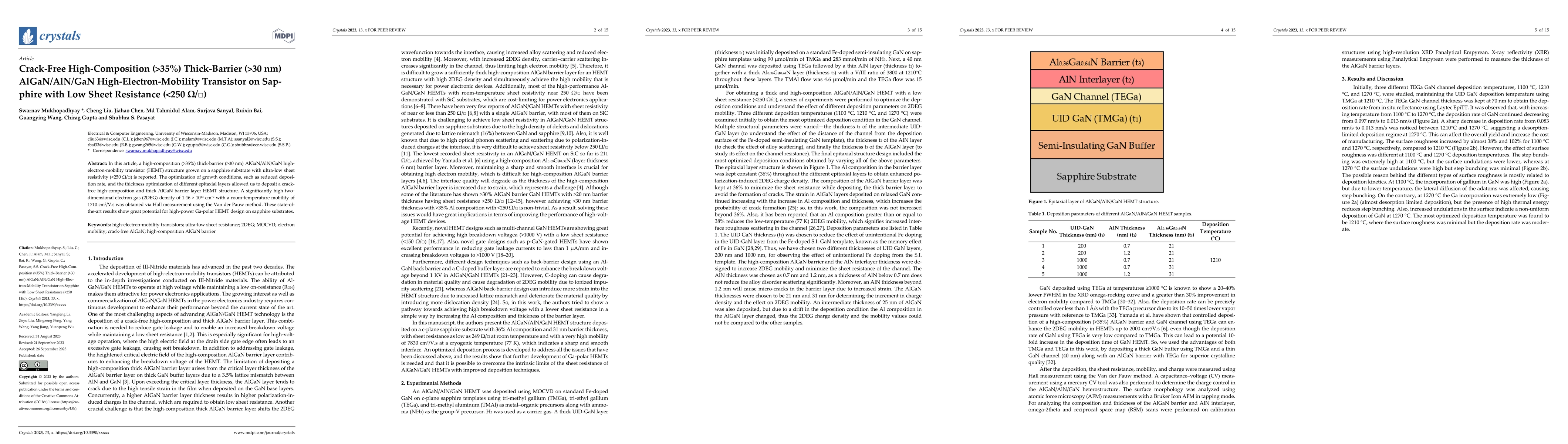
In this article, high composition (>35%) thick (>30 nm) barrier AlGaN/AlN/GaN HEMT structure grown on a sapphire substrate with ultra-low sheet resistivity (<250 \Omega / \Box ) is reported. Optimiz...

Thumbnail for Tera-sample-per-second arbitrary waveform generation in the synthetic
  dimension

Tera-sample-per-second arbitrary waveform generation in the synthetic dimension

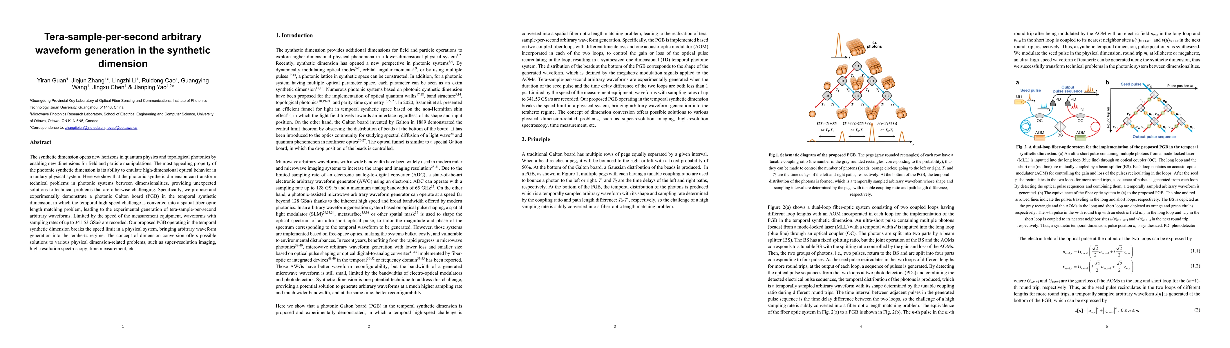
The synthetic dimension opens new horizons in quantum physics and topological photonics by enabling new dimensions for field and particle manipulations. The most appealing property of the photonic s...

Thumbnail for Parity-time symmetry in wavelength space with spatial singularity

Parity-time symmetry in wavelength space with spatial singularity

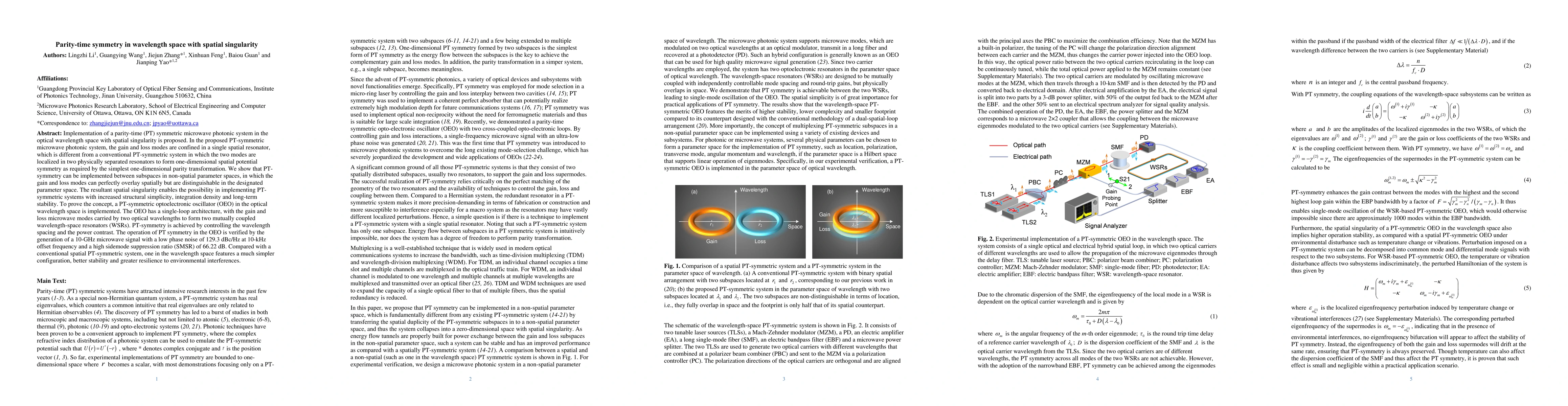
Implementation of a parity-time (PT) symmetric microwave photonic system in the optical wavelength space with spatial singularity is proposed. In the proposed PT-symmetric microwave photonic system,...

Thumbnail for Demonstration of Si-doped Al-rich thin regrown Al(Ga)N films on AlN on
  sapphire templates with $\gt10^{15}/cm^3$ free carrier concentration using
  close-coupled showerhead MOCVD reactor

Demonstration of Si-doped Al-rich thin regrown Al(Ga)N films on AlN on sapphire templates with $\gt10^{15}/cm^3$ free carrier concentration using close-coupled showerhead MOCVD reactor

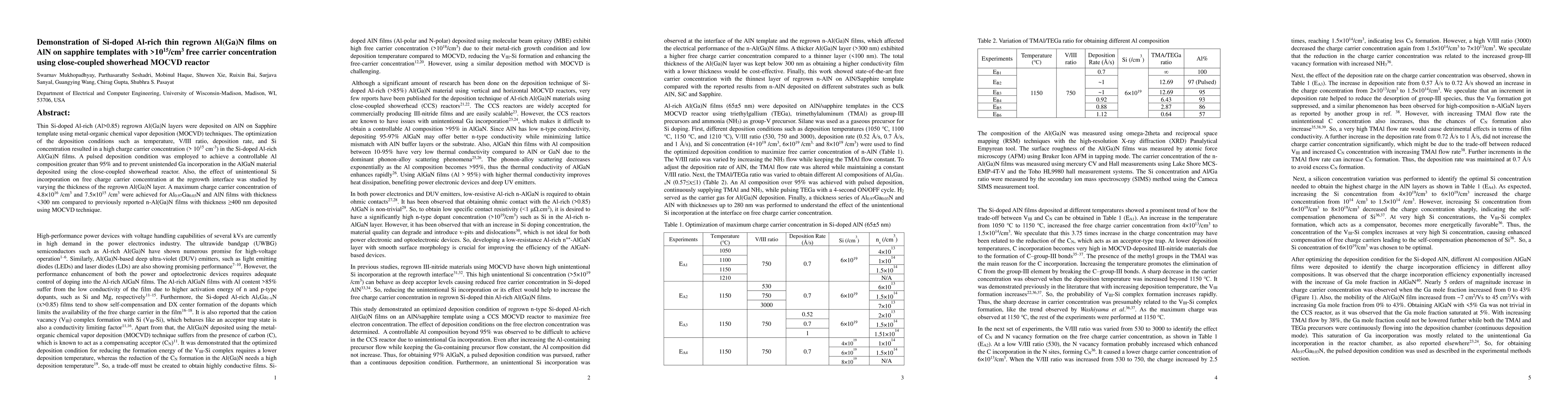
Thin Si-doped Al-rich (Al>0.85) regrown Al(Ga)N layers were deposited on AlN on Sapphire template using metal-organic chemical vapor deposition (MOCVD) techniques. The optimization of the deposition c...

Thumbnail for Electrical Characterization of High-k (k>115) Crystalline SrTiO3 (STO) thin film integration with GaN with Nanomembrane Transfer Process

Electrical Characterization of High-k (k>115) Crystalline SrTiO3 (STO) thin film integration with GaN with Nanomembrane Transfer Process

High-k (115), crystalline SrTiO3 (STO) thin film was transferred on GaN for potential applications in power devices (transistor and diodes) by nanomembrane transfer method and the detailed electrical ...

Thumbnail for Single-crystalline high-quality beta-Ga2O3 pseudo-substrate on sapphire through sputtering for epitaxial deposition

Single-crystalline high-quality beta-Ga2O3 pseudo-substrate on sapphire through sputtering for epitaxial deposition

Solid-phase epitaxy (SPE) of beta-Ga2O3 thin films by radio-frequency (RF) sputtering and then crystallized through high-temperature post-deposition annealing is employed on sapphire substrates, yield...

This website uses cookies to ensure you get the best experience. Learn more