Academic Profile
Statistics
Similar Authors
Papers on arXiv
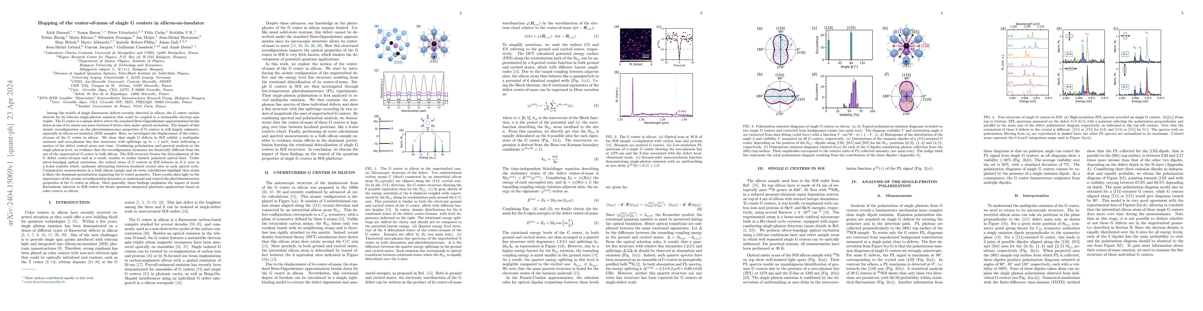
Among the wealth of single fluorescent defects recently detected in silicon, the G center catches interest for its telecom single-photon emission that could be coupled to a metastable electron spin ...
Boron nitride (BN) is today considered as one of the most promising materials for many novel applications including bright single photon emission, deep UV opto-electronics, small sized solid-state n...
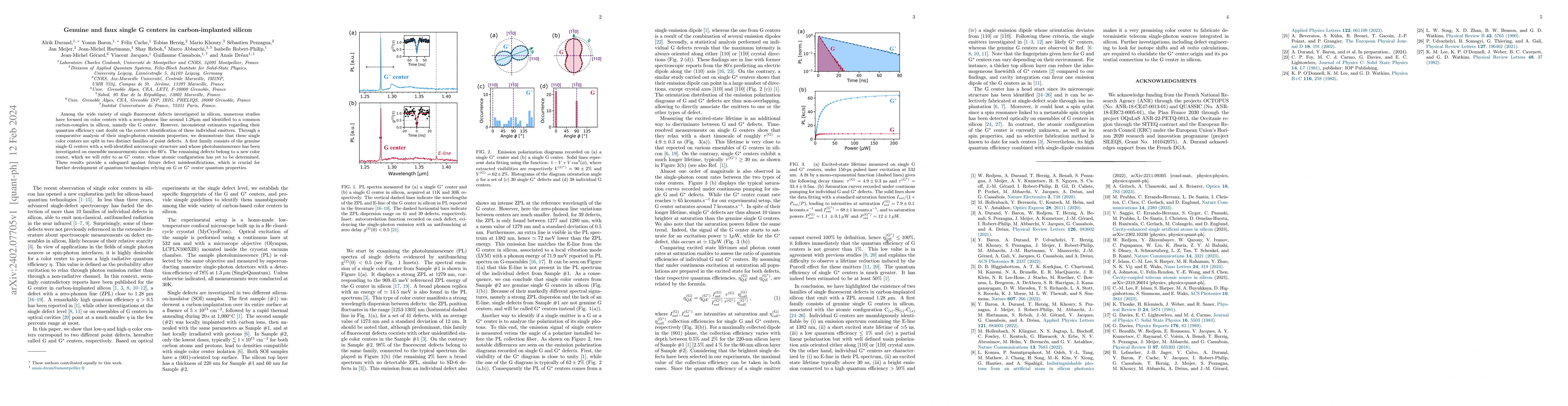
Among the wide variety of single fluorescent defects investigated in silicon, numerous studies have focused on color centers with a zero-phonon line around $1.28 \mu$m and identified to a common car...
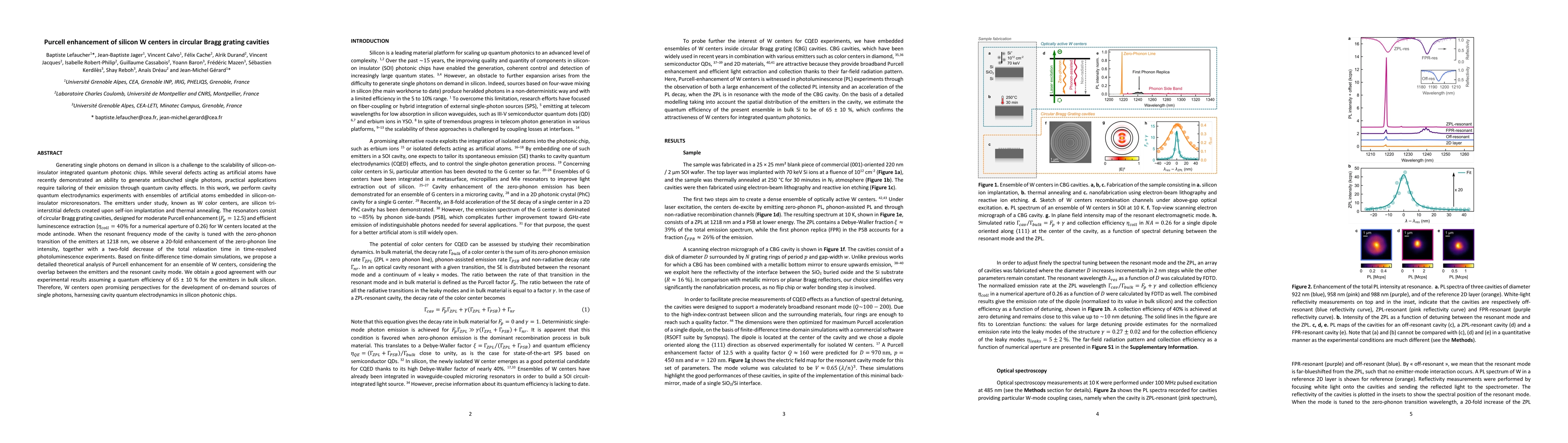
Generating single photons on demand in silicon is a challenge to the scalability of silicon-on-insulator integrated quantum photonic chips. While several defects acting as artificial atoms have rece...
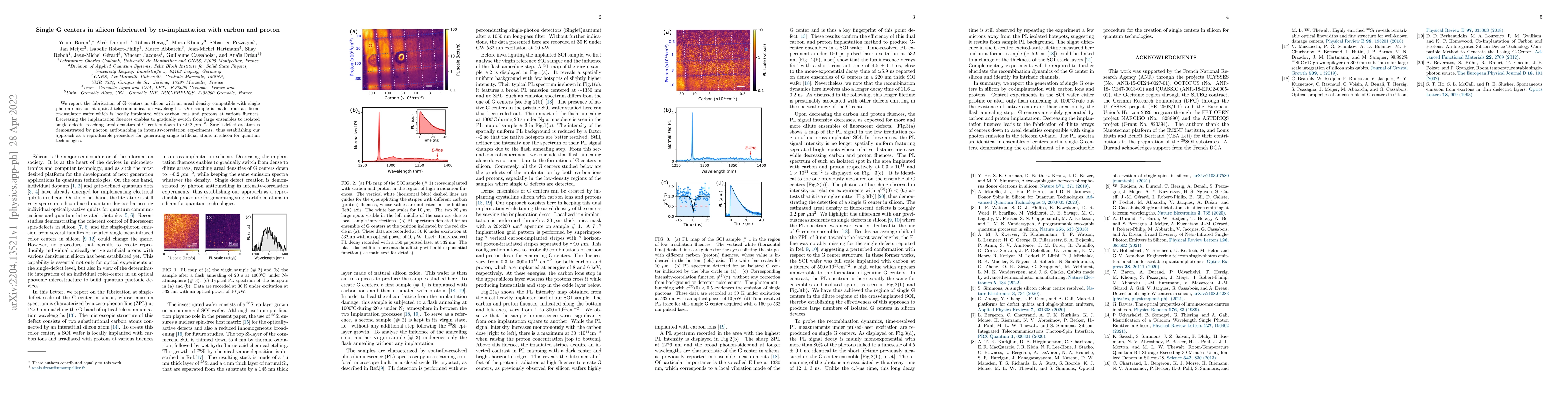
We report the fabrication of G centers in silicon with an areal density compatible with single photon emission at optical telecommunication wavelengths. Our sample is made from a silicon-on-insulato...
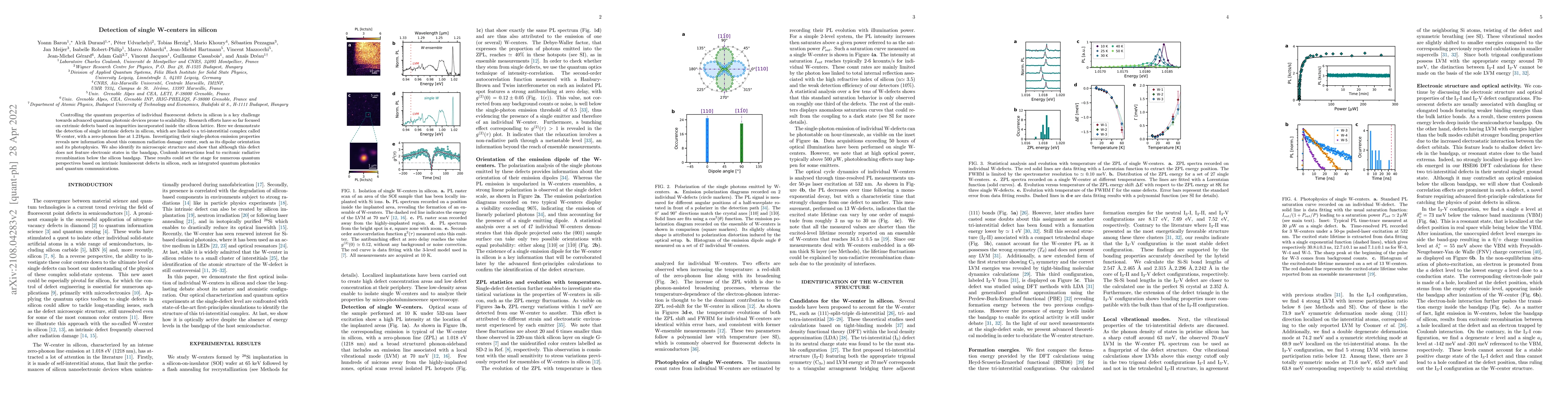
Controlling the quantum properties of individual fluorescent defects in silicon is a key challenge towards advanced quantum photonic devices prone to scalability. Research efforts have so far focuse...
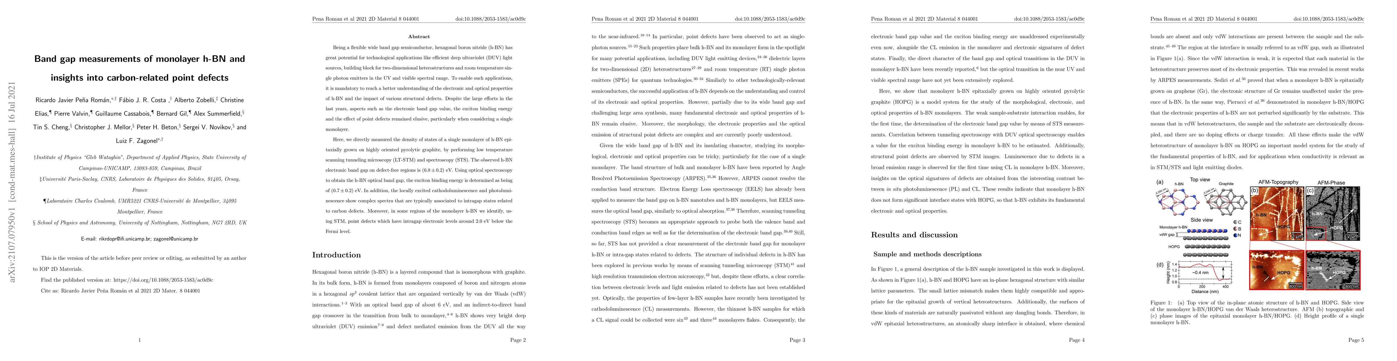
Being a flexible wide band gap semiconductor, hexagonal boron nitride (h-BN) has great potential for technological applications like efficient deep ultraviolet light sources, building block for two-...
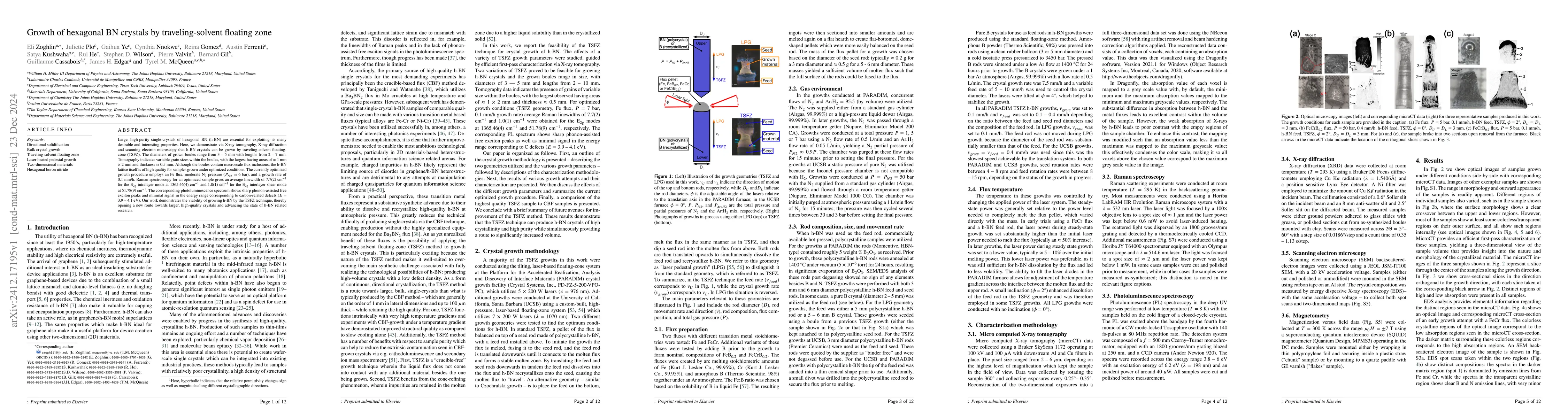
Large, high-purity single-crystals of hexagonal BN (h-BN) are essential for exploiting its many desirable and interesting properties. Here, we demonstrate via X-ray tomography, X-ray diffraction and s...
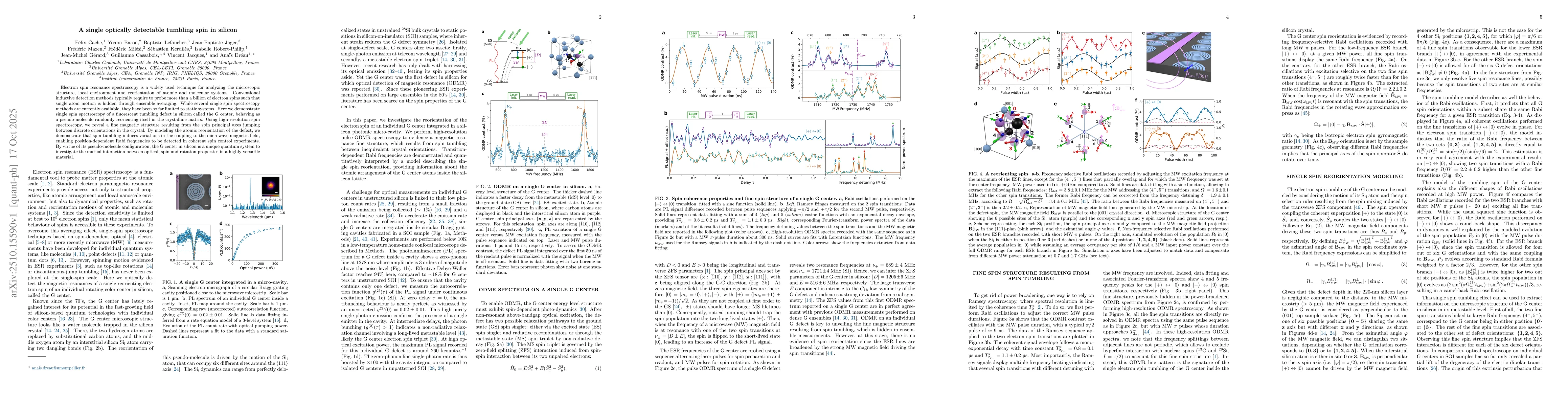
Electron spin resonance spectroscopy is a widely used technique for analyzing the microscopic structure, local environment and reorientation of atomic and molecular systems. Conventional inductive det...
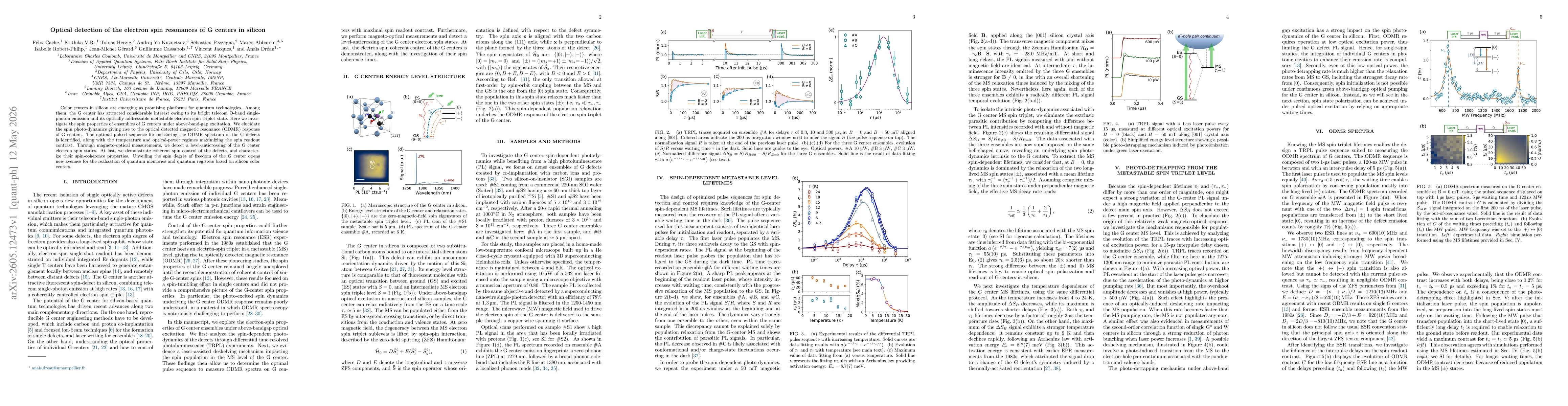
Color centers in silicon are emerging as promising platforms for quantum technologies. Among them, the G center has attracted considerable interest owing to its bright telecom O-band single-photon emi...
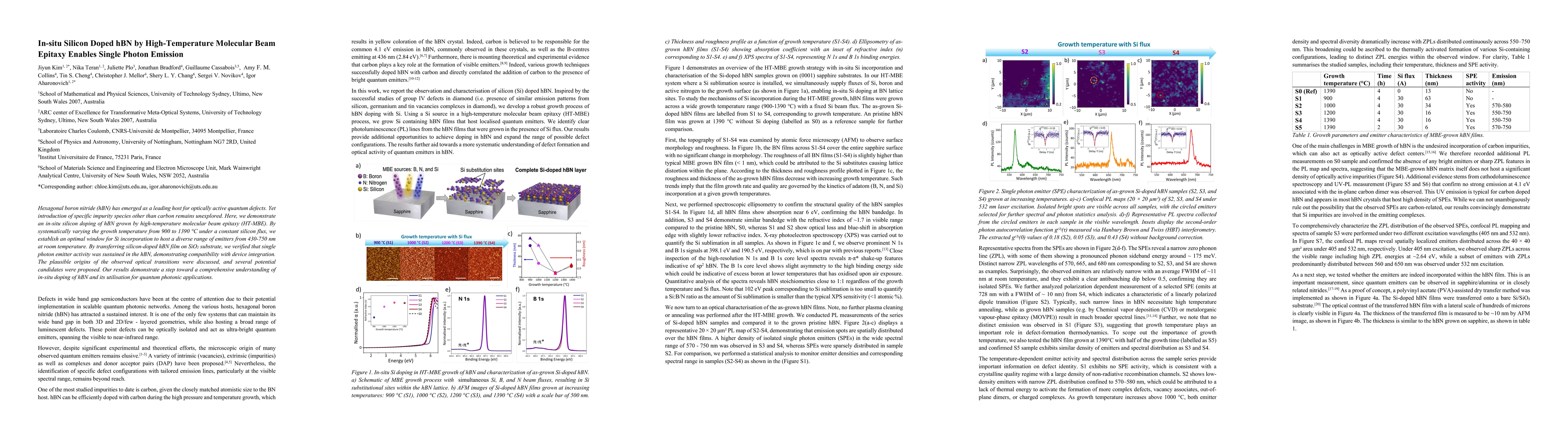
Hexagonal boron nitride (hBN) has emerged as a leading host for optically active quantum defects. Yet introduction of specific impurity species other than carbon remains unexplored. Here, we demonstra...