Academic Profile
Statistics
Similar Authors
Papers on arXiv
In the presence of high magnetic field, quantum Hall systems usually host both even- and odd-integer quantized states because of lifted band degeneracies. Selective control of these quantized states...
Moir\'e superlattices have emerged as a new platform for studying strongly correlated quantum phenomena, but these systems have been largely limited to van der Waals layer two-dimensional (2D) mater...
We thank G.P. Mikitik and Yu.V. Sharlai for contributing this note and the cordial exchange about it. First and foremost, we note that the aim of our paper is to report a methodology to diagnose top...
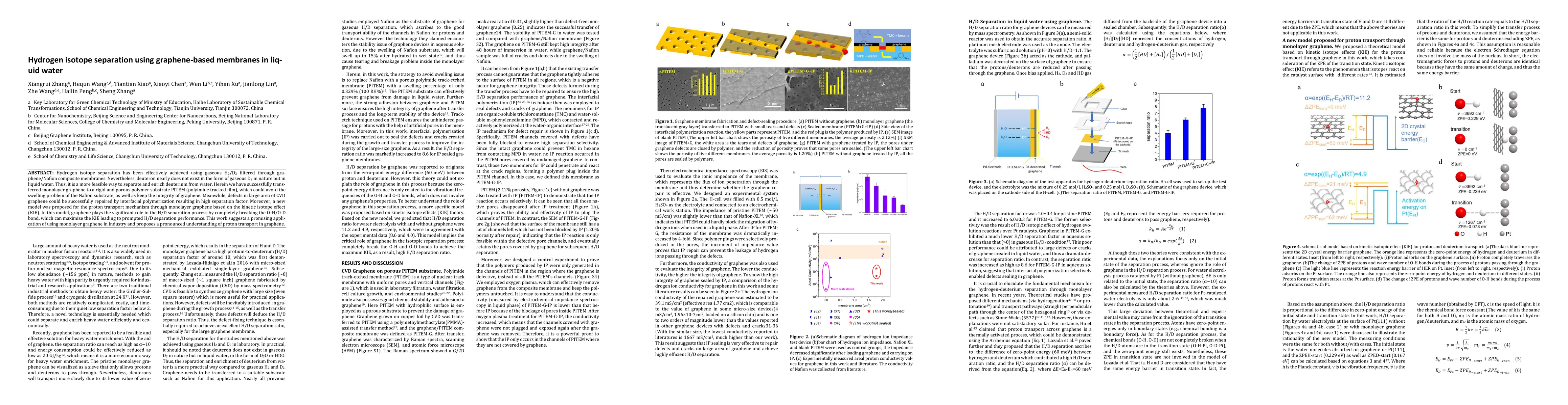
Hydrogen isotope separation has been effectively achieved using gaseous H2/D2 filtered through graphene/Nafion composite membranes. Nevertheless, deuteron nearly does not exist in the form of gaseou...
Systematic electrical transport characterizations were performed on high-quality Bi2O2Se nanowires to illustrate its great transport properties and further application potentials in spintronics. Bi2...
We report on an experimental study of the effect of coherent surface-bulk electron scattering on quantum transport in a three-dimensional topological insulator Bi$_2$Te$_3$ nanoplate. The nanoplate ...
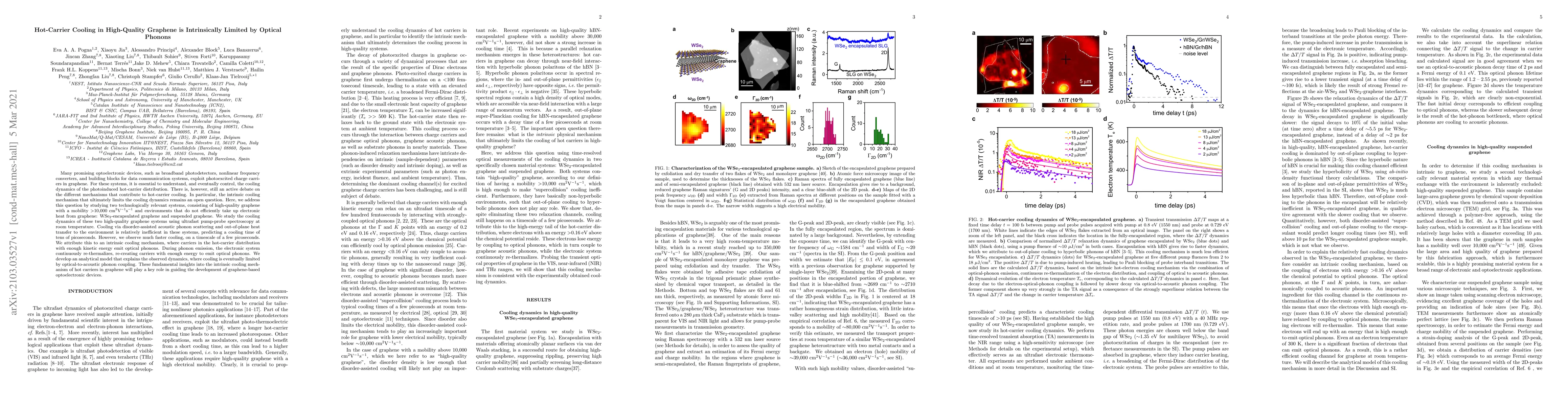
Many promising optoelectronic devices, such as broadband photodetectors, nonlinear frequency converters, and building blocks for data communication systems, exploit photoexcited charge carriers in g...
The capture of photoexcited deep-band hot carriers, excited by photons with energies far above the bandgap, is of significant importance for photovoltaic and photoelectronic applications since it is...
We report on realization and quantum transport study of a twisted bilayer graphene (tBLG) Josephson junction device. High-quality tBLG employed in the device fabrication is obtained via chemical vap...
Stacking order has strong influence on the coupling between the two layers of twisted bilayer graphene (BLG), which in turn determines its physical properties. Here, we report the investigation of t...
The phase offset of quantum oscillations is commonly used to experimentally diagnose topologically non-trivial Fermi surfaces. This methodology, however, is inconclusive for spin-orbit-coupled metal...
Quantum confined devices of three-dimensional topological insulators have been proposed to be promising and of great importance for studies of confined topological states and for applications in low...
We study a relativistic quantum cavity system realized by etching out from a graphene sheet by quantum transport measurements and theoretical calculations. The conductance of the graphene cavity has...
Topological physics has evolved from its initial focus on fermionic systems to the exploration of bosonic systems, particularly phononic excitations in crystalline materials. Two-dimensional (2D) topo...
Quantized conductance in quasi-one-dimensional systems not only provides a hallmark of ballistic transport, but also serves as a gateway for exploring quantum phenomena. Recently, a unique hidden Rash...
The recent progress in nanosheet transistors has established two-dimensional (2D) semiconductors as viable candidates for future ultra-scaled electronic devices. Next to reducing contact resistance, i...
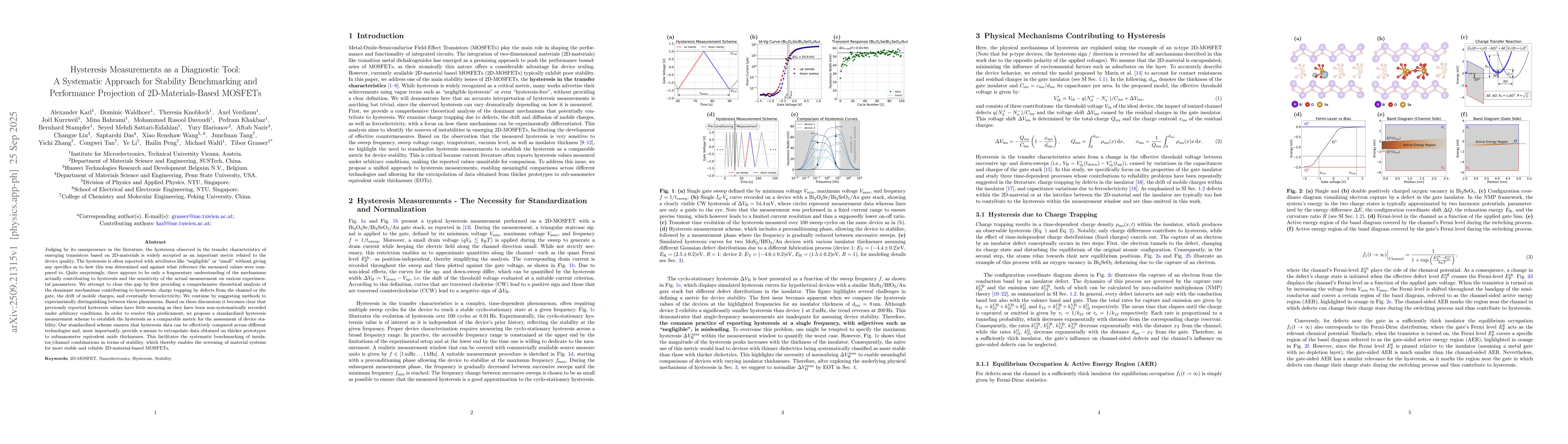
Judging by its omnipresence in the literature, the hysteresis observed in the transfer characteristics of emerging transistors based on 2D-materials is widely accepted as an important metric related t...
Hexagonal boron nitride (hBN) supports a wide range of two-dimensional (2D) technologies, yet assessing its crystalline quality over large areas remains a fundamental challenge. Both antiparallel doma...
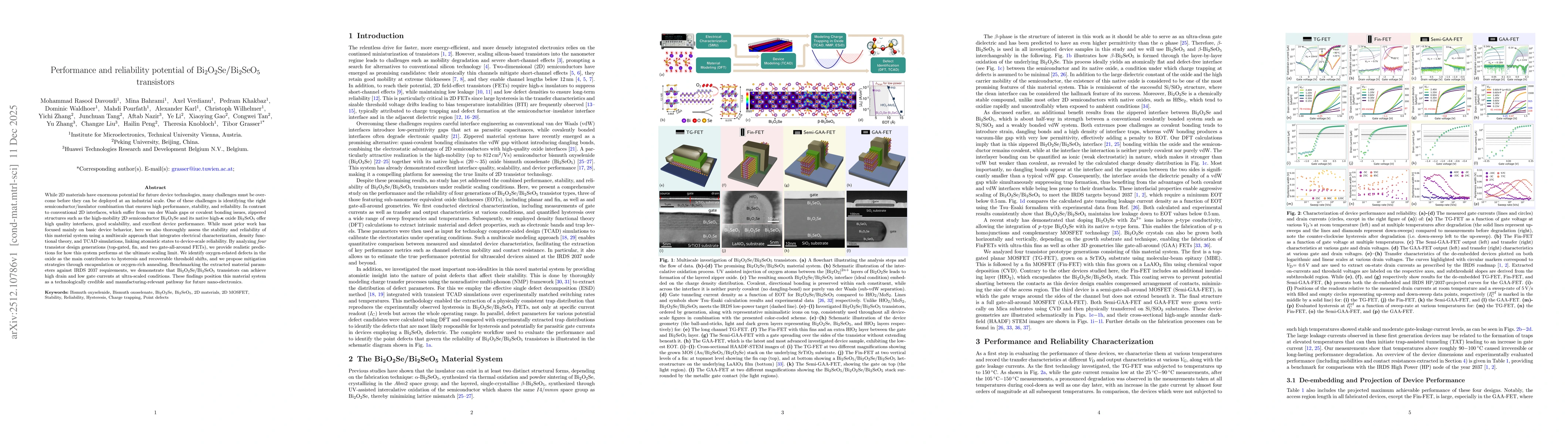
While 2D materials have enormous potential for future device technologies, many challenges must be overcome before they can be deployed at an industrial scale. One of these challenges is identifying t...