Academic Profile
Statistics
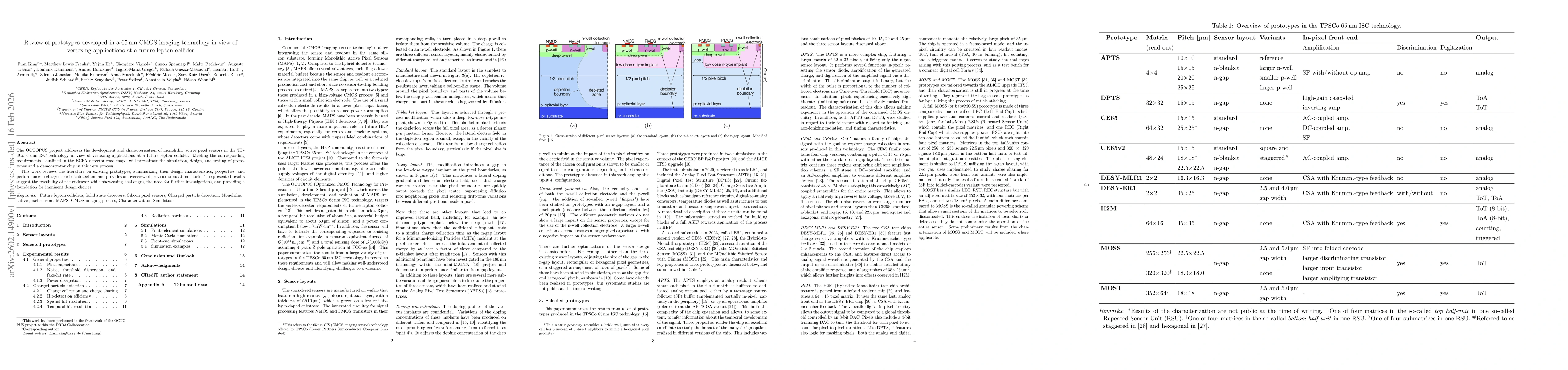
Similar Authors
Papers on arXiv
Monolithic active pixel sensors (MAPS) produced in a 65 nm CMOS imaging technology are being investigated for applications in particle physics. The MAPS design has a small collection electrode chara...
Monolithic CMOS sensors in a 65 nm imaging technology are being investigated by the CERN EP Strategic R&D Programme on Technologies for Future Experiments for an application in particle physics. The...
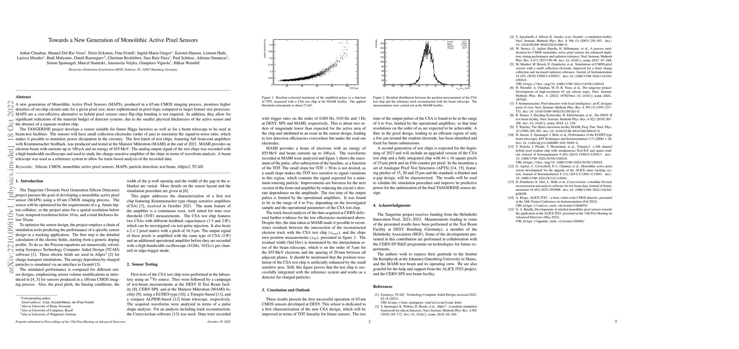
A new generation of Monolithic Active Pixel Sensors (MAPS), produced in a 65 nm CMOS imaging process, promises higher densities of on-chip circuits and, for a given pixel size, more sophisticated in...
The Tangerine project aims to develop new state-of-the-art high-precision silicon detectors. Part of the project has the goal of developing a monolithic active pixel sensor using a novel 65 nm CMOS ...
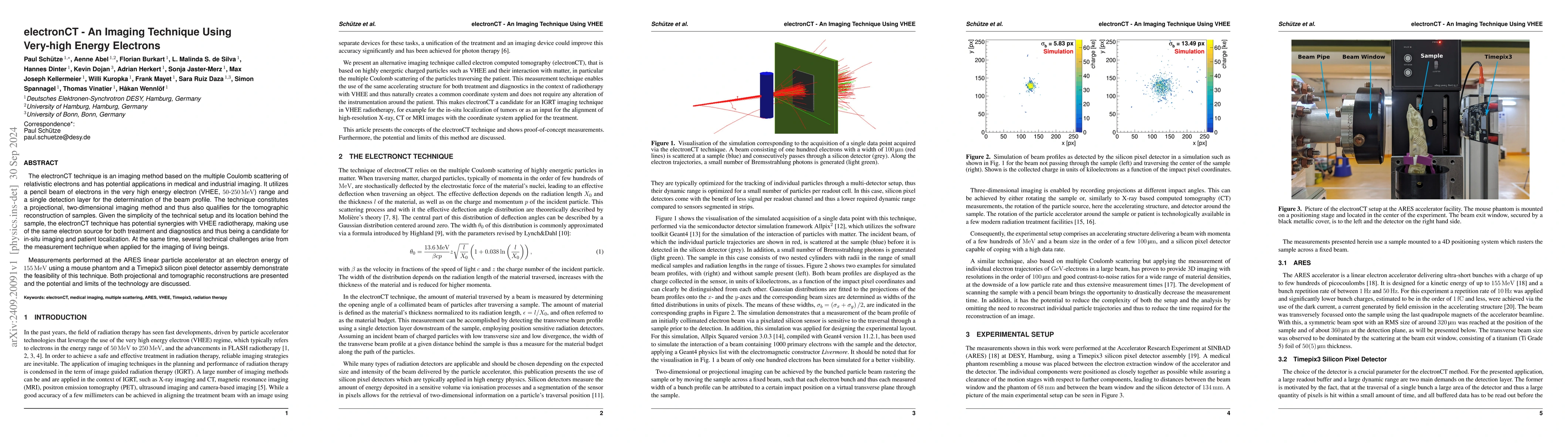
The electronCT technique is an imaging method based on the multiple Coulomb scattering of relativistic electrons and has potential applications in medical and industrial imaging. It utilizes a pencil ...
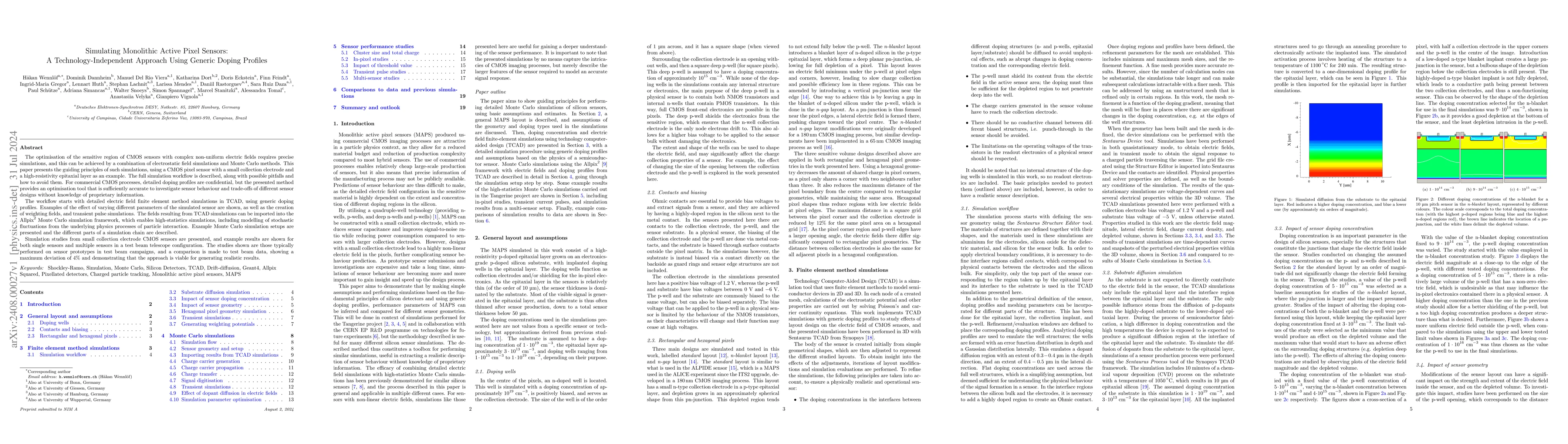
The optimisation of the sensitive region of CMOS sensors with complex non-uniform electric fields requires precise simulations, and this can be achieved by a combination of electrostatic field simulat...
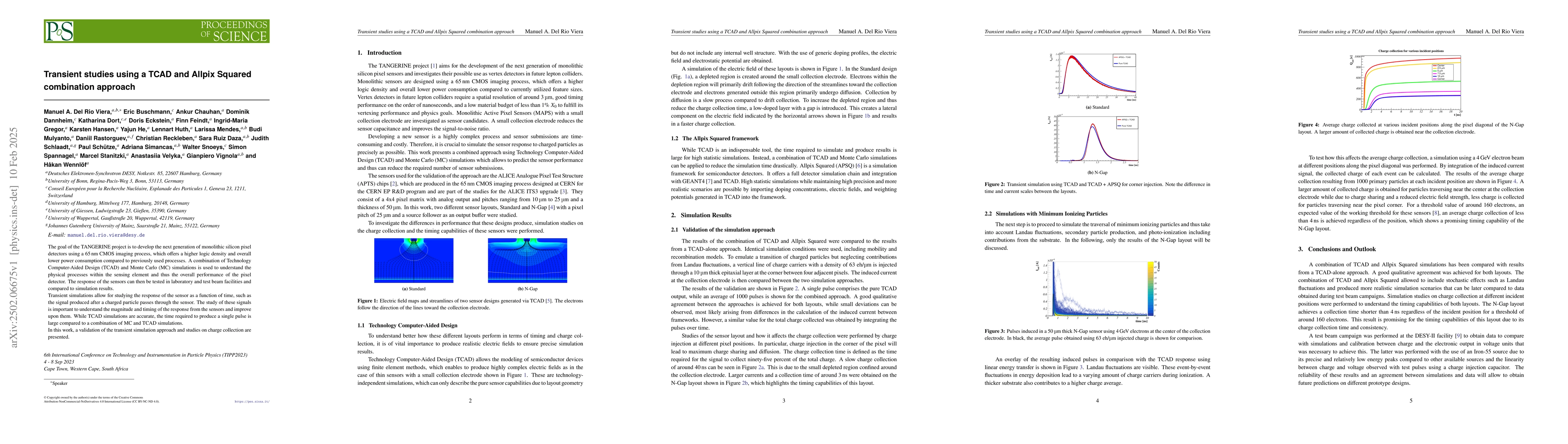
The goal of the TANGERINE project is to develop the next generation of monolithic silicon pixel detectors using a 65 nm CMOS imaging process, which offers a higher logic density and overall lower powe...
The high energy physics community recently gained access to the TPSCo 65 nm ISC (Image Sensor CMOS), which enables a higher in-pixel logic density in monolithic active pixel sensors (MAPS) compared to...
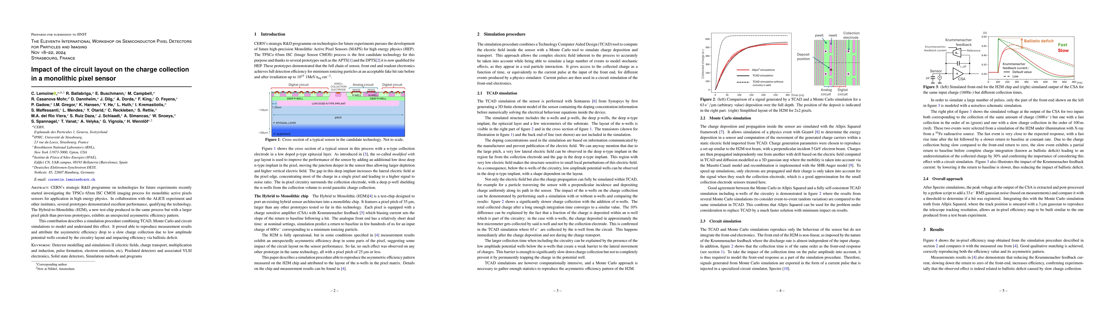
CERN's strategic R&D programme on technologies for future experiments recently started investigating the TPSCo 65nm ISC CMOS imaging process for monolithic active pixels sensors for application in hig...
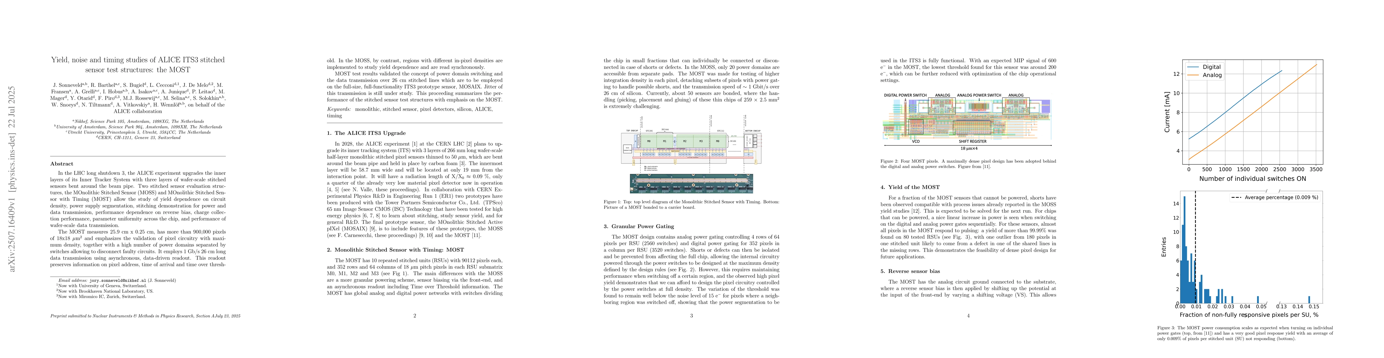
In the LHC long shutdown 3, the ALICE experiment upgrades the inner layers of its Inner Tracker System with three layers of wafer-scale stitched sensors bent around the beam pipe. Two stitched sensor ...
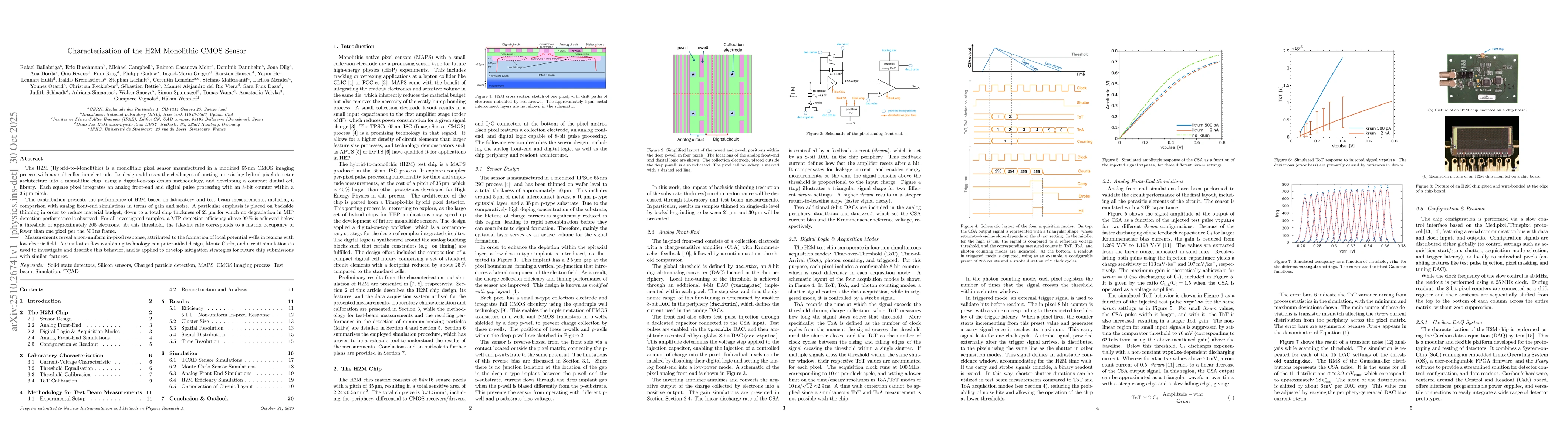
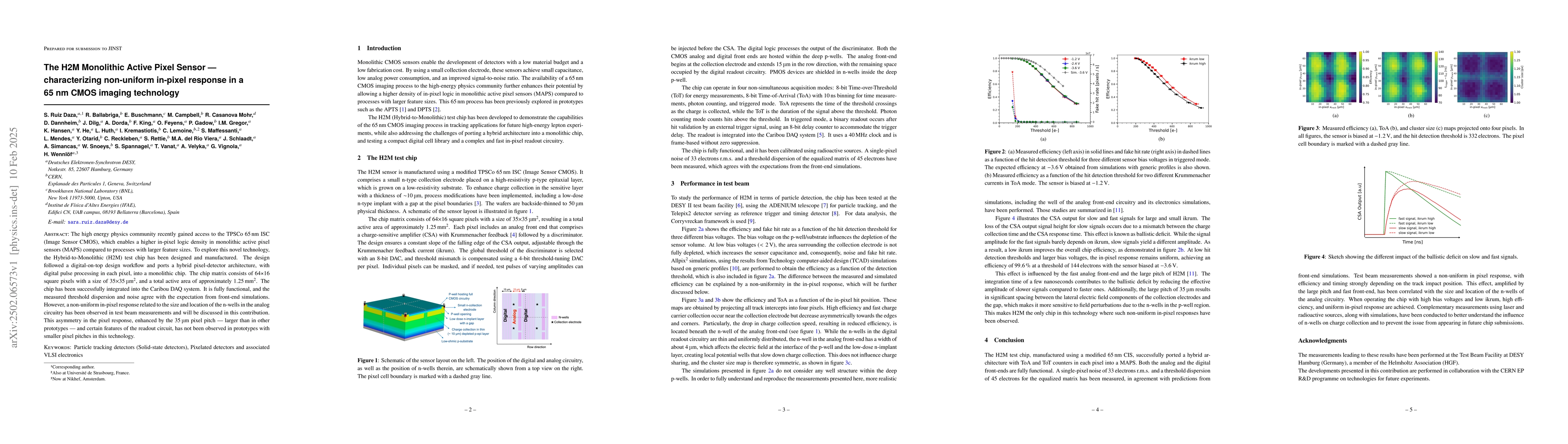
The H2M (Hybrid-to-Monolithic) is a monolithic pixel sensor manufactured in a modified \SI{65}{\nano\meter}~CMOS imaging process with a small collection electrode. Its design addresses the challenges ...
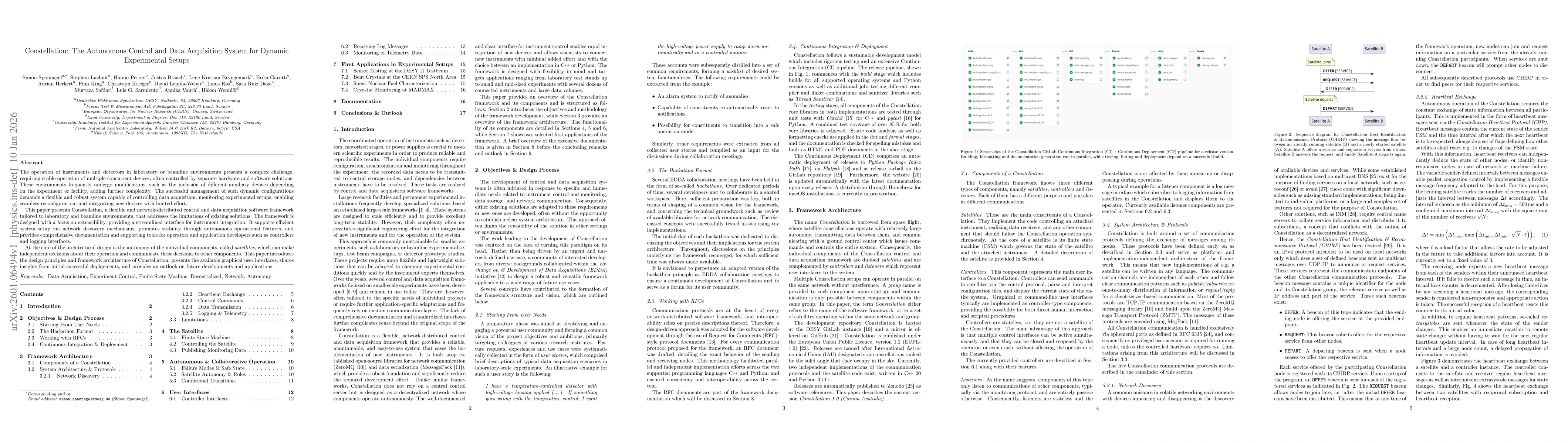
The operation of instruments and detectors in laboratory or beamline environments presents a complex challenge, requiring stable operation of multiple concurrent devices, often controlled by separate ...
The OCTOPUS project addresses the development and characterization of monolithic active pixel sensors in the TPSCo 65 nm ISC technology in view of vertexing applications at a future lepton collider. M...