Academic Profile
Statistics
Similar Authors
Papers on arXiv
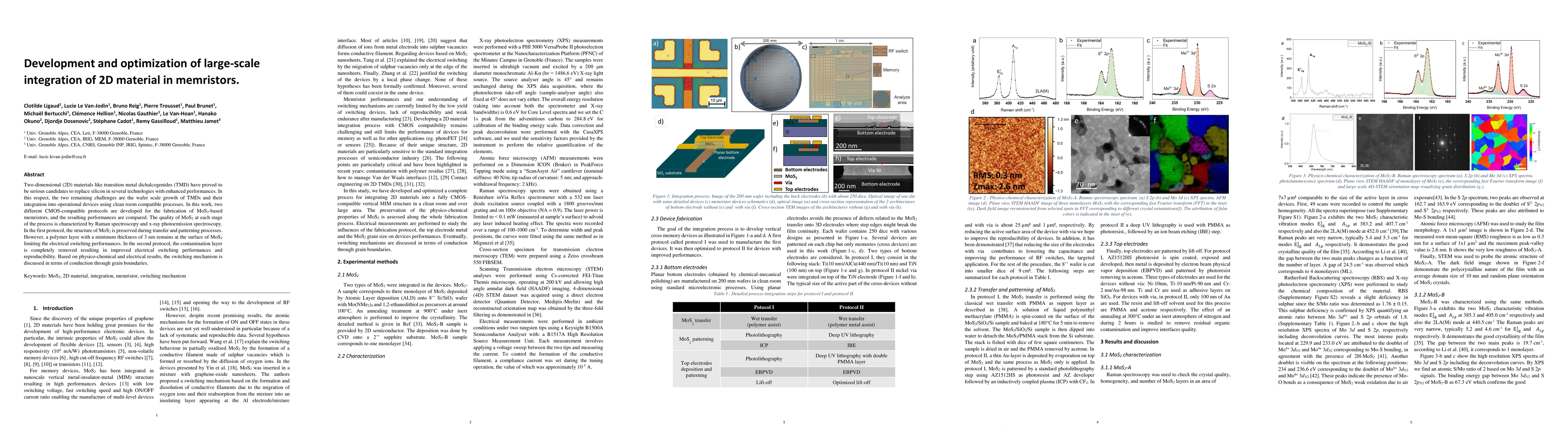
Two-dimensional (2D) materials like transition metal dichalcogenides (TMD) have proved to be serious candidates to replace silicon in several technologies with enhanced performances. In this respect...
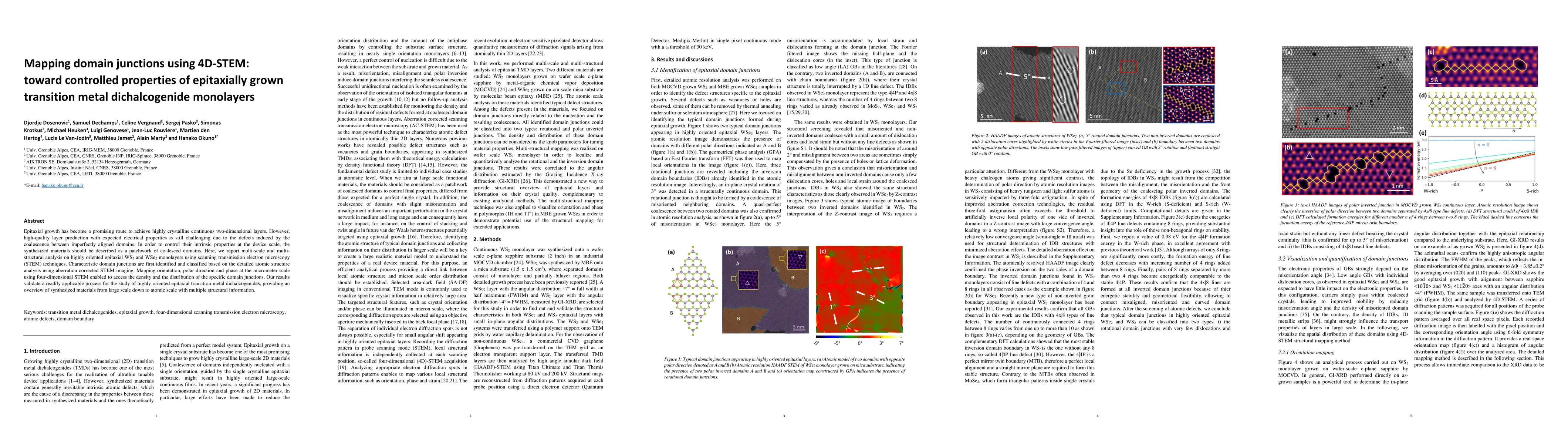
Epitaxial growth has become a promising route to achieve highly crystalline continuous two-dimensional layers. However, high-quality layer production with expected electrical properties is still cha...
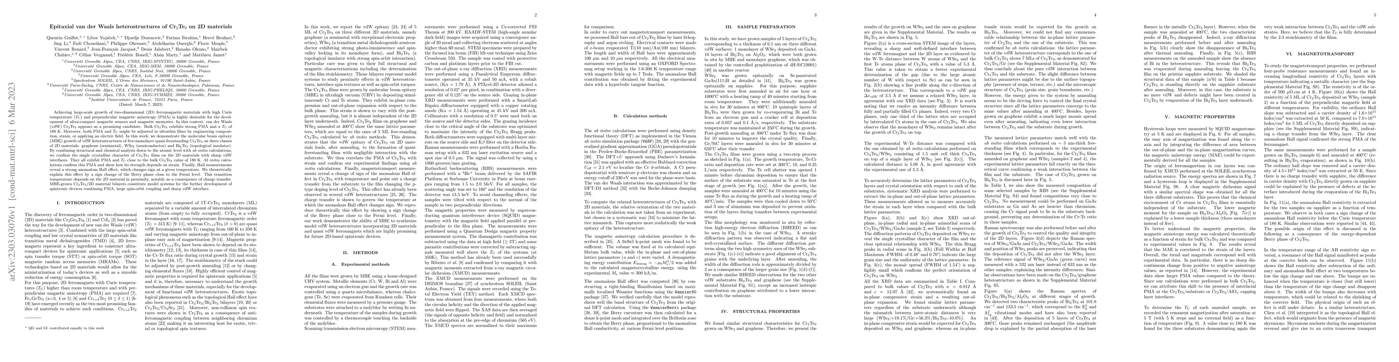
Achieving large-scale growth of two-dimensional (2D) ferromagnetic materials with high Curie temperature (TC) and perpendicular magnetic anisotropy (PMA) is highly desirable for the development of u...
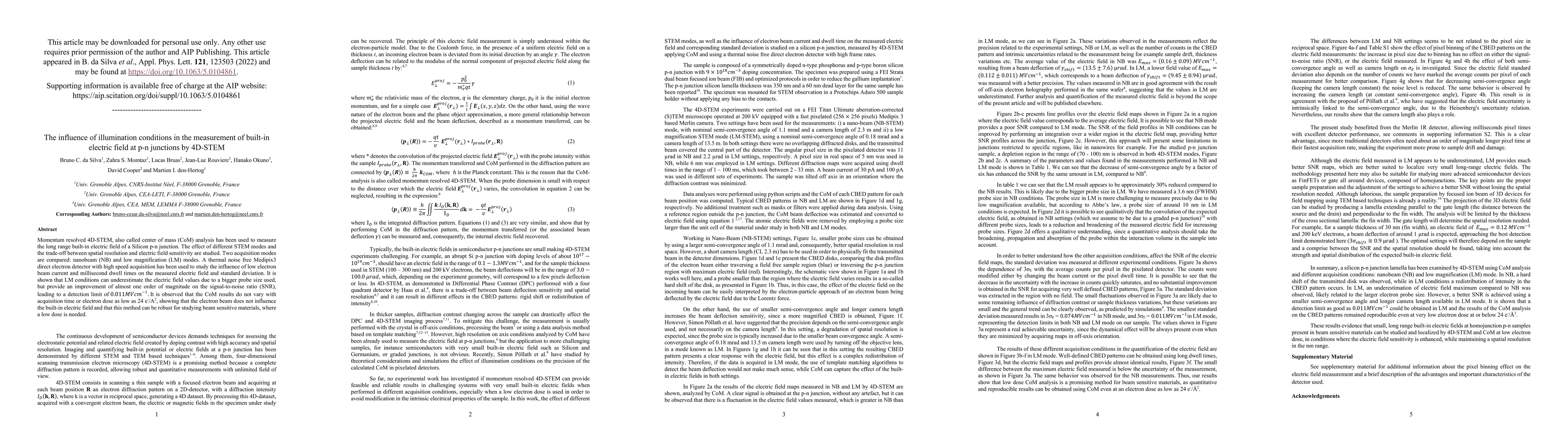
Momentum resolved 4D-STEM, also called center of mass (CoM) analysis, has been used to measure the long range built-in electric field of a silicon p-n junction. The effect of different STEM modes an...
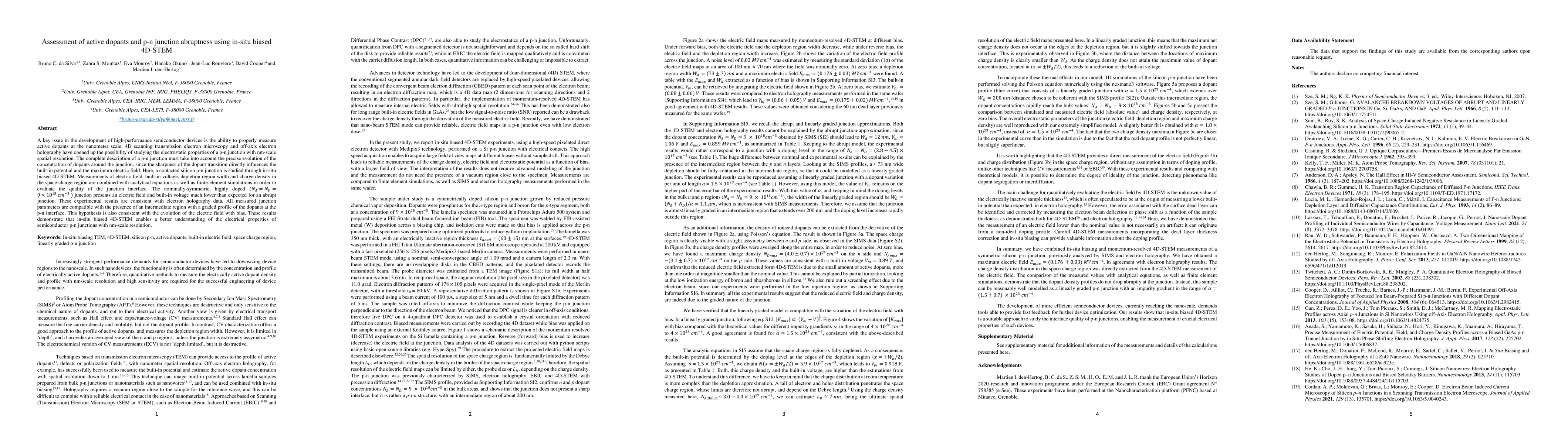
A key issue in the development of high-performance semiconductor devices is the ability to properly measure active dopants at the nanometer scale. 4D scanning transmission electron microscopy and of...
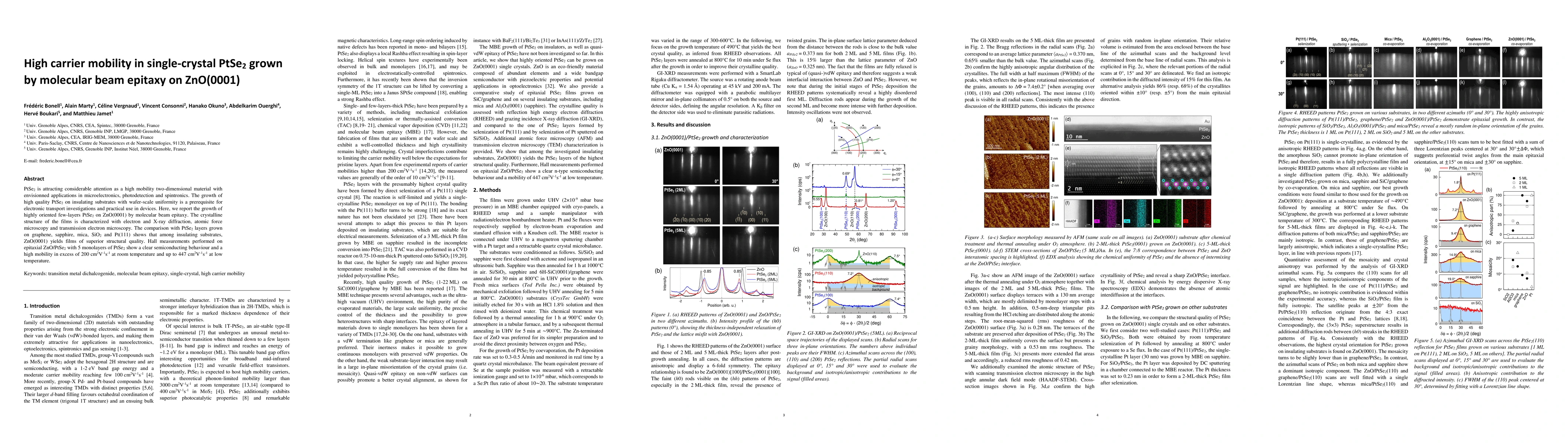
PtSe2 is attracting considerable attention as a high mobility two-dimensional material with envisionned applications in microelectronics, photodetection and spintronics. The growth of high quality P...
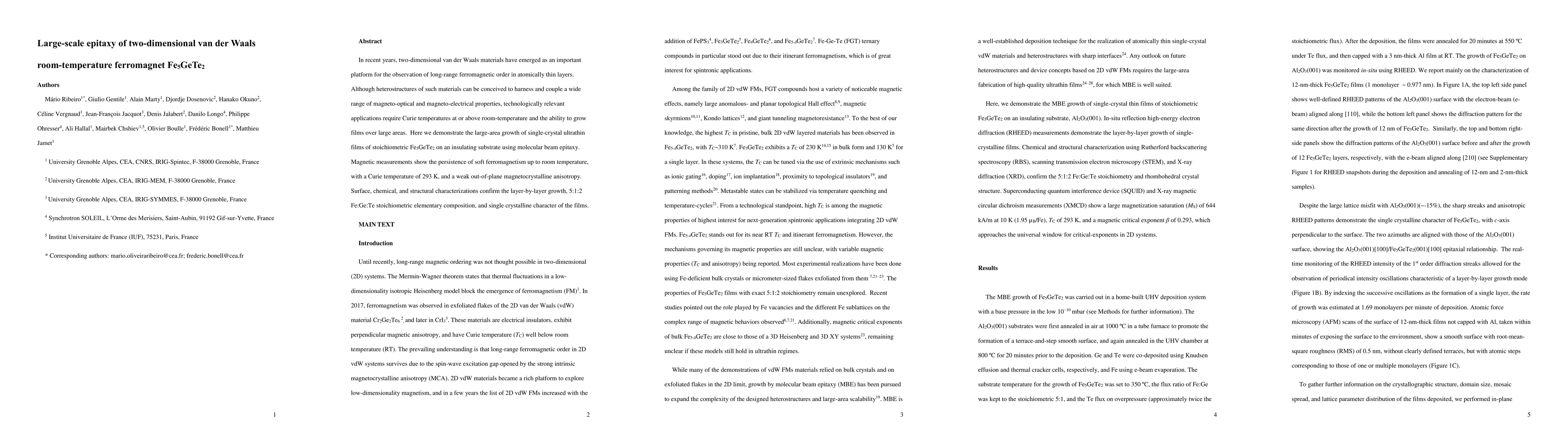
In recent years, two-dimensional van der Waals materials have emerged as an important platform for the observation of long-range ferromagnetic order in atomically thin layers. Although heterostructu...
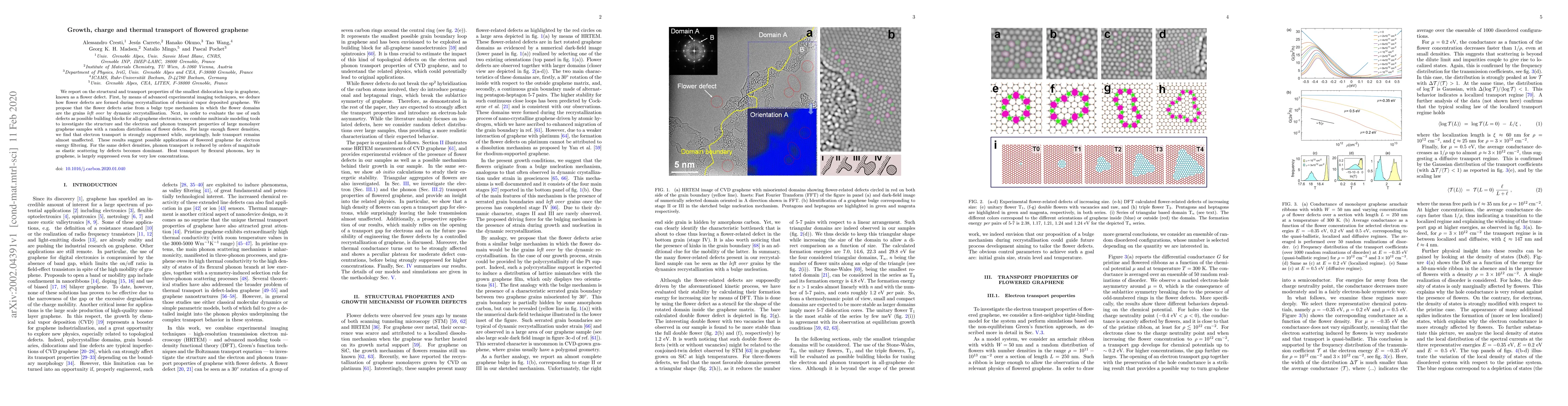
We report on the structural and transport properties of the smallest dislocation loop in graphene, known as a flower defect. First, by means of advanced experimental imaging techniques, we deduce ho...
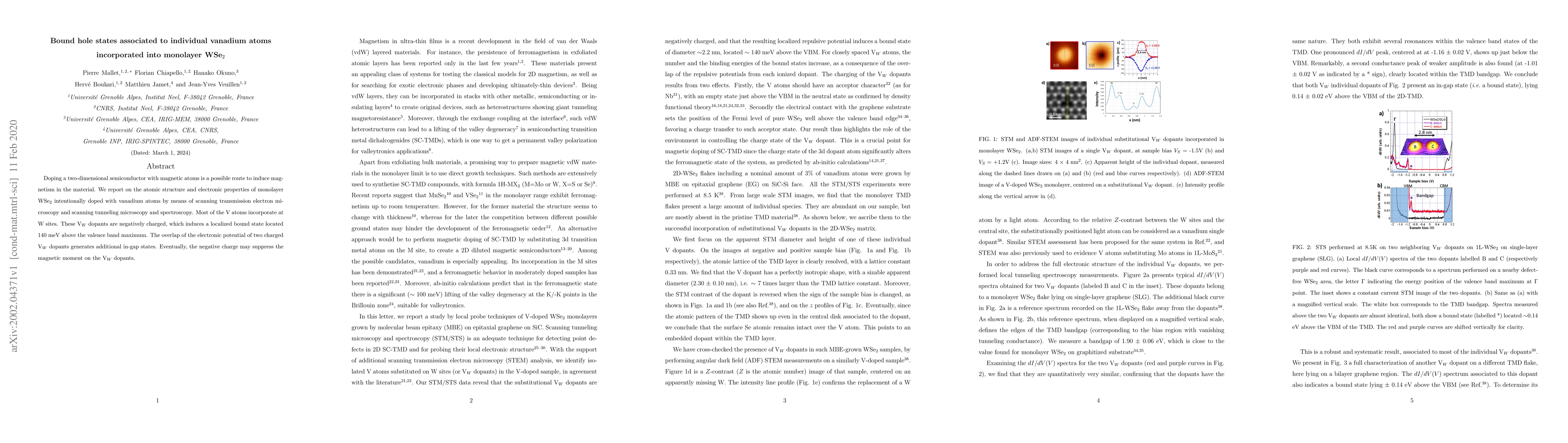
Doping a two-dimensional semiconductor with magnetic atoms is a possible route to induce magnetism in the material. We report on the atomic structure and electronic properties of monolayer WSe$_2$ i...
The search for high-quality transition metal dichalcogenides mono- and multi-layers grown on large areas is still a very active field of investigation nowadays. Here, we use molecular beam epitaxy t...
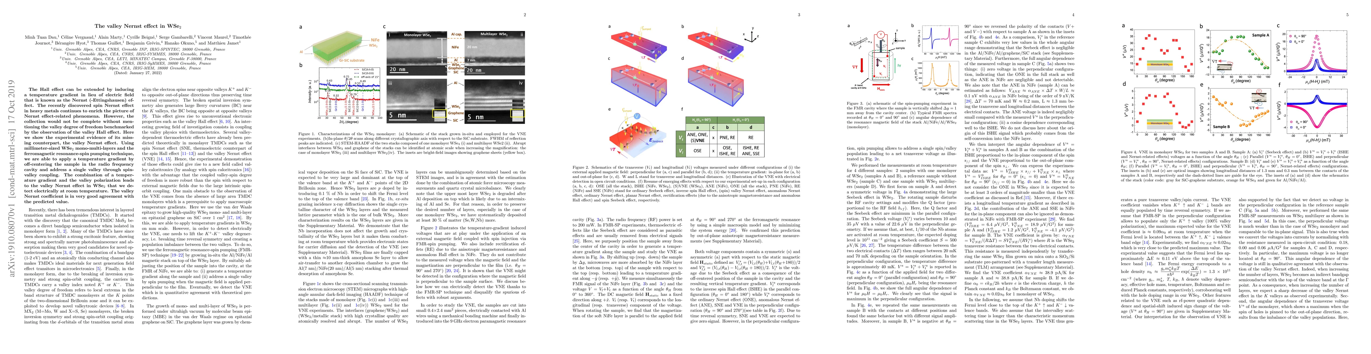
The Hall effect can be extended by inducing a temperature gradient in lieu of electric field that is known as the Nernst (-Ettingshausen) effect. The recently discovered spin Nernst effect in heavy ...
Two-dimensional PtSe2 exhibits outstanding intrinsic properties such as high carrier mobility, tunable bandgap, broadband absorption and air stability, making it ideal for (opto)electronic application...
Single wall carbon nanotubes (SWCNT) exhibit remarkable optical and electrical properties making them one of the most promising materials for next generation electronic and optoelectronic devices. The...
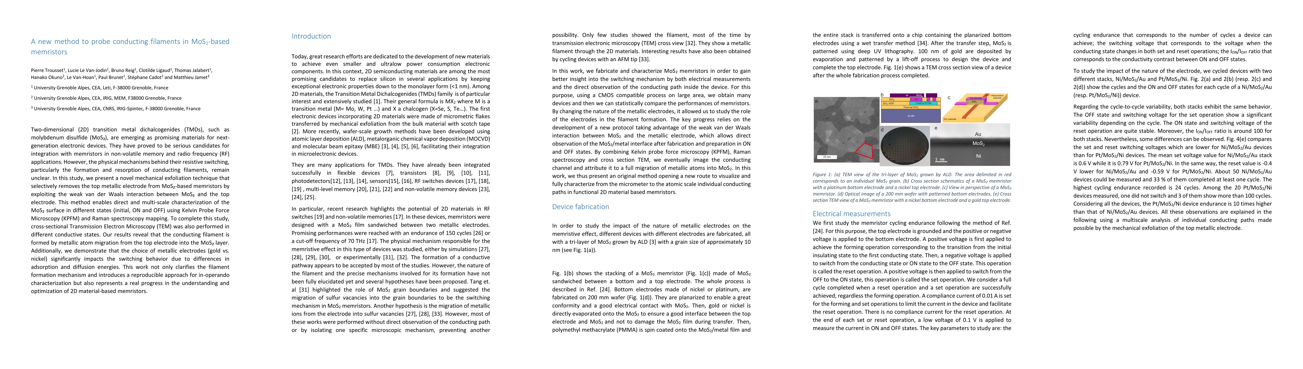
Two-dimensional (2D) transition metal dichalcogenides (TMDs), such as molybdenum disulfide (MoS$_2$), are emerging as promising materials for next-generation electronic devices. They have proved to be...