Academic Profile
Statistics
Similar Authors
Papers on arXiv
Ultrathin ferroelectric films with out-of-plane polarization and high Curie temperatures are key to miniaturizing electronic devices. Most ferroelectrics employed in devices are proper ferroelectrics,...
Modern electromechanical actuators and sensors rely on the piezoelectric effect that linearly couples strain and electric polarization. However, this effect is restricted to materials that lack invers...
Microscopy is a primary source of information on materials structure and functionality at nanometer and atomic scales. The data generated is often well-structured, enriched with metadata and sample hi...
With the decreasing sizes of integrated-circuit components, the semiconductor industry is in growing need of high-throughput strain mapping techniques that offer high precision and spatial resolution,...
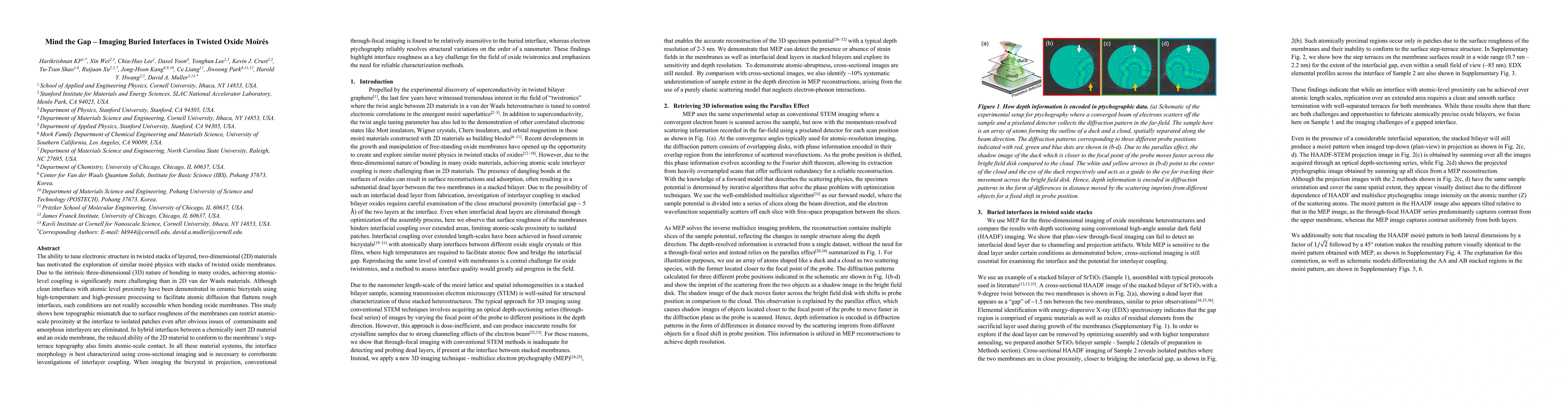
The ability to tune electronic structure in twisted stacks of layered, two-dimensional (2D) materials has motivated the exploration of similar moir\'e physics with stacks of twisted oxide membranes. D...
Scaling ferroelectrics to nanometer thicknesses remains a central challenge for low-power, nonvolatile electronics, as leakage currents increasingly dominate with reduced dimensions. Alkali-based, lea...