Academic Profile
Statistics
Similar Authors
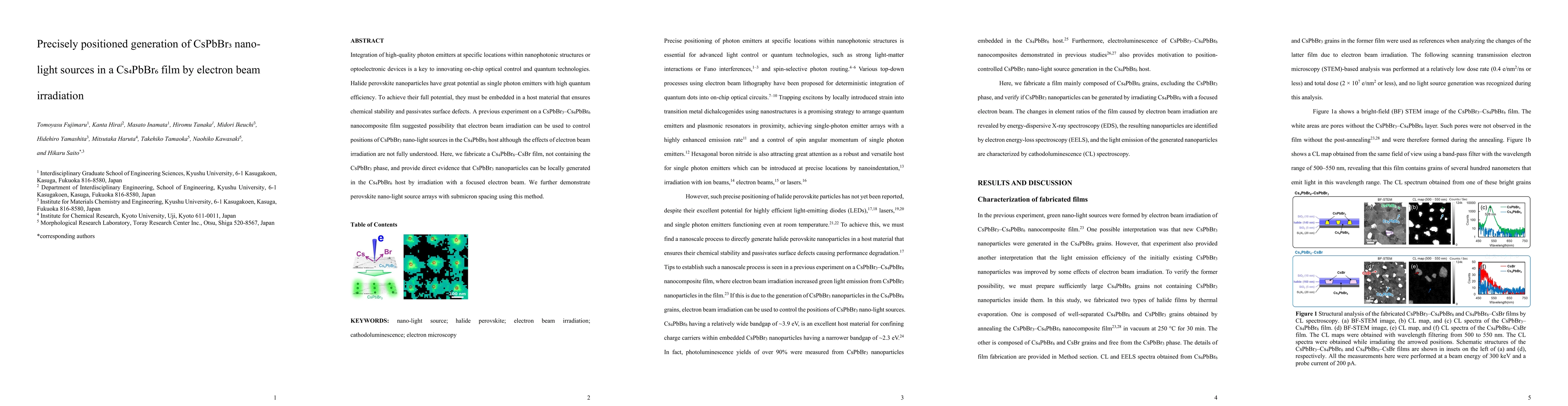
Papers on arXiv
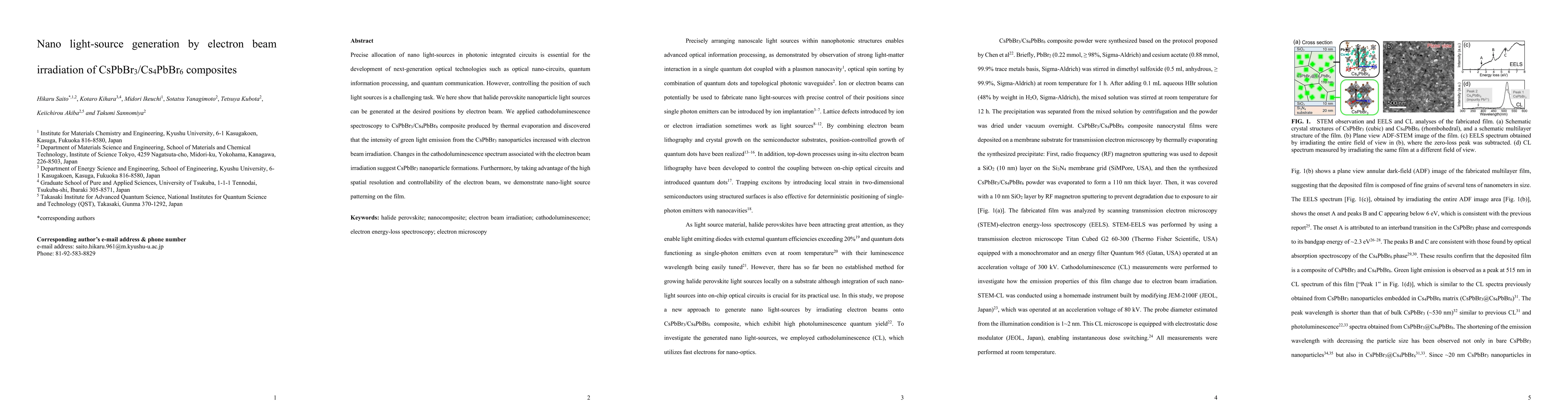
Electron microscopy based on high-energy electrons allows nanoscopic analytical imaging taking advantage of secondarily generated particles. Especially for cathodoluminescence, the correlation betwe...
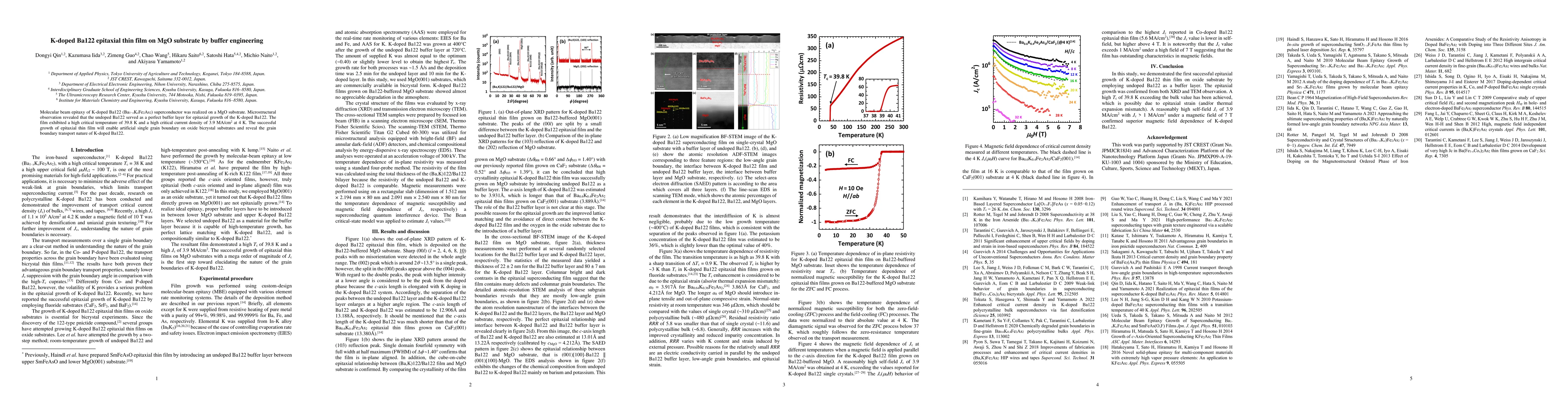
Molecular beam epitaxy of K-doped Ba122 (Ba$_{1-x}$K$_x$Fe$_\text{2}$As$_\text{2}$) superconductor was realized on a MgO substrate. Microstructural observation revealed that the undoped Ba122 served...
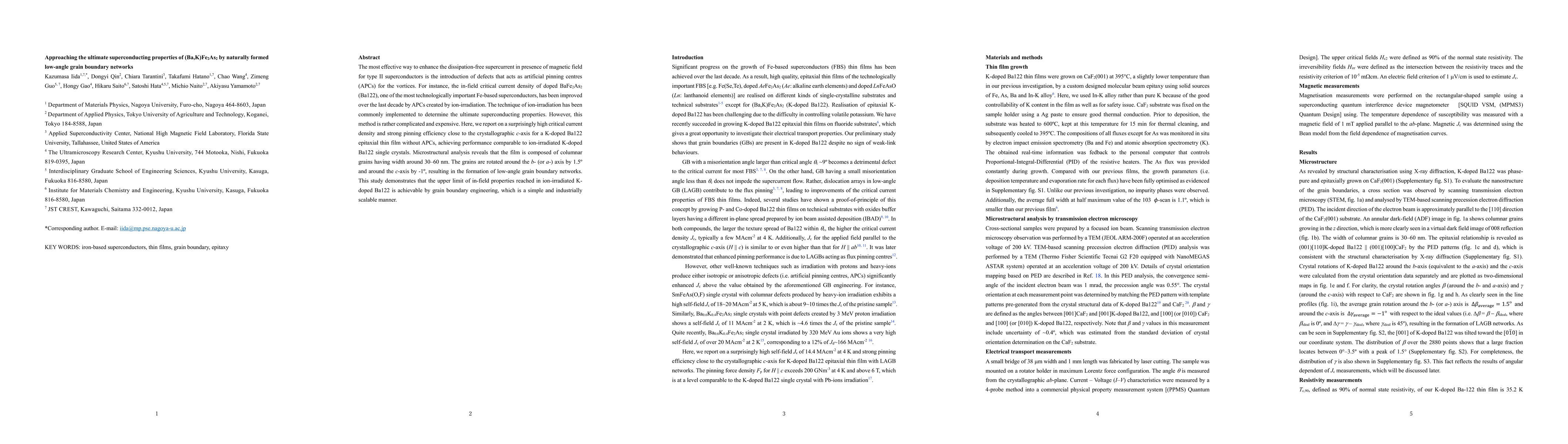
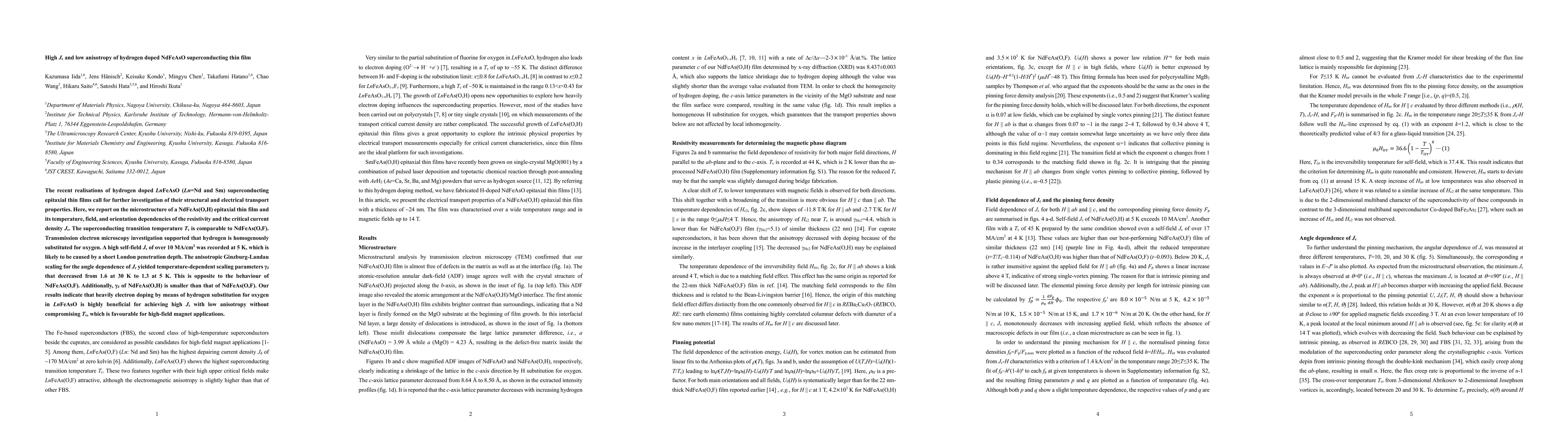
The most effective way to enhance the dissipation-free supercurrent in presence of magnetic field for type II superconductors is the introduction of defects that acts as artificial pinning centres (...
The recent realisations of hydrogen doped $Ln$FeAsO ($Ln$=Nd and Sm) superconducting epitaxial thin films call for further investigation of their structural and electrical transport properties. Here...
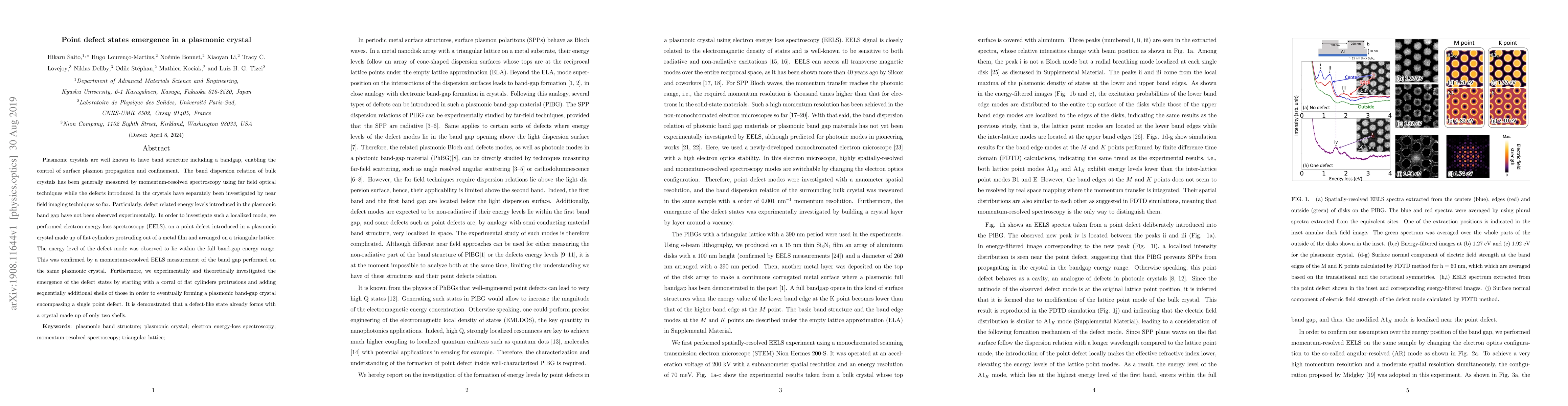
Plasmonic crystals are well known to have band structure including a bandgap, enabling the control of surface plasmon propagation and confinement. The band dispersion relation of bulk crystals has b...
Precise allocation of nano light-sources in photonic integrated circuits is essential for the development of next-generation optical technologies such as optical nano-circuits, quantum information pro...
Integration of high-quality photon emitters at specific locations within nanophotonic structures or optoelectronic devices is a key to innovating on-chip optical control and quantum technologies. Hali...