Academic Profile
Statistics
Similar Authors
Papers on arXiv
Two-dimensional (2D) materials are considered for numerous applications in microelectronics, although several challenges remain when integrating them into functional devices. Weak adhesion is one of...
We demonstrate the design, fabrication, and characterization of wafer-scale, zero-bias power detectors based on two-dimensional MoS$_2$ field effect transistors (FETs). The MoS$_2$ FETs are fabricat...
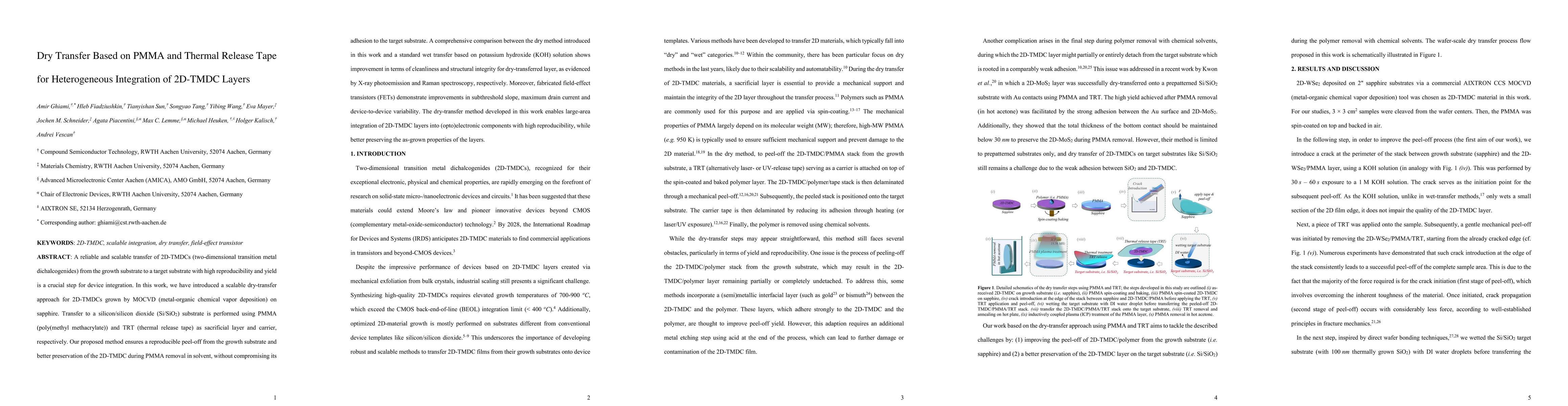
A reliable and scalable transfer of 2D-TMDCs (two-dimensional transition metal dichalcogenides) from the growth substrate to a target substrate with high reproducibility and yield is a crucial step fo...
Layered two-dimensional (2D) semiconductors have shown enhanced ion migration capabilities along their van der Waals (vdW) gaps and on their surfaces. This effect can be employed for resistive switchi...
Two-dimensional materials (2DMs) have been widely investigated because of their potential for heterogeneous integration with modern electronics. However, several major challenges remain, such as the d...
Two-dimensional material (2DM)-based field-effect transistors (FETs), such as molybdenum disulfide (MoS${_2}$)-FETs, have gained significant attention for their potential for ultra-short channels, the...
Developing electronic devices capable of emulating biological functions is essential for advancing brain-inspired computation paradigms such as neuromorphic computing. In recent years, two-dimensional...
Memristors based on two-dimensional materials (2DMs) have garnered significant attention due to their fast resistive switching (RS) behavior and atomic-level thickness, which enables low power consump...