Academic Profile
Statistics
Similar Authors
Papers on arXiv
The lack of p-type doping has impeded the development of vertical gallium oxide (Ga2O3) devices. Current blocking layers (CBL) using implanted deep acceptors has been used to demonstrate vertical de...
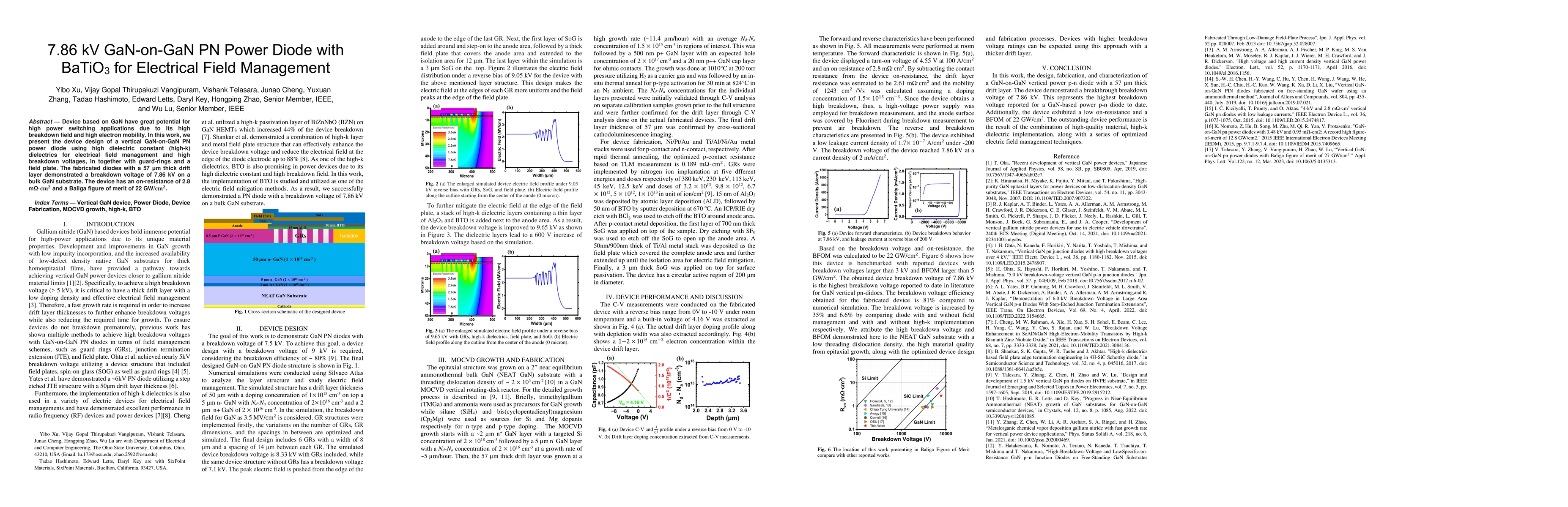
Device based on GaN have great potential for high power switching applications due to its high breakdown field and high electron mobility. In this work, we present the device design of a vertical Ga...
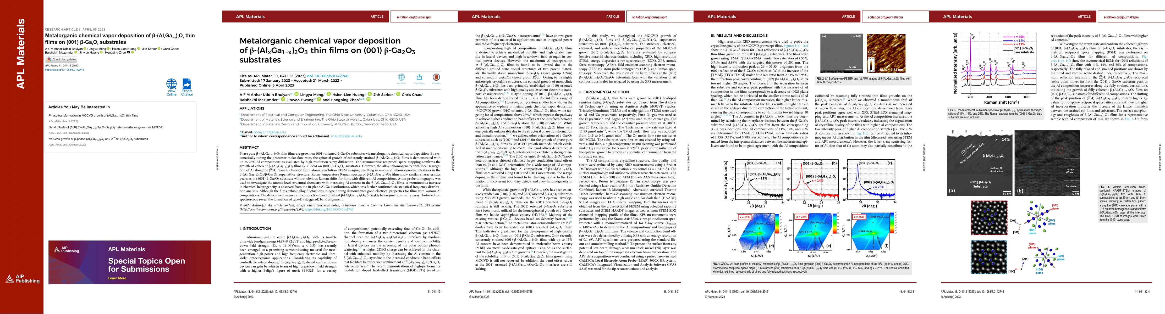
Phase pure \b{eta}-(AlxGa1-x)2O3 thin films are grown on (001) oriented \b{eta}-Ga2O3 substrates via metalorganic chemical vapor deposition (MOCVD). By systematically tuning the precursor molar flow...
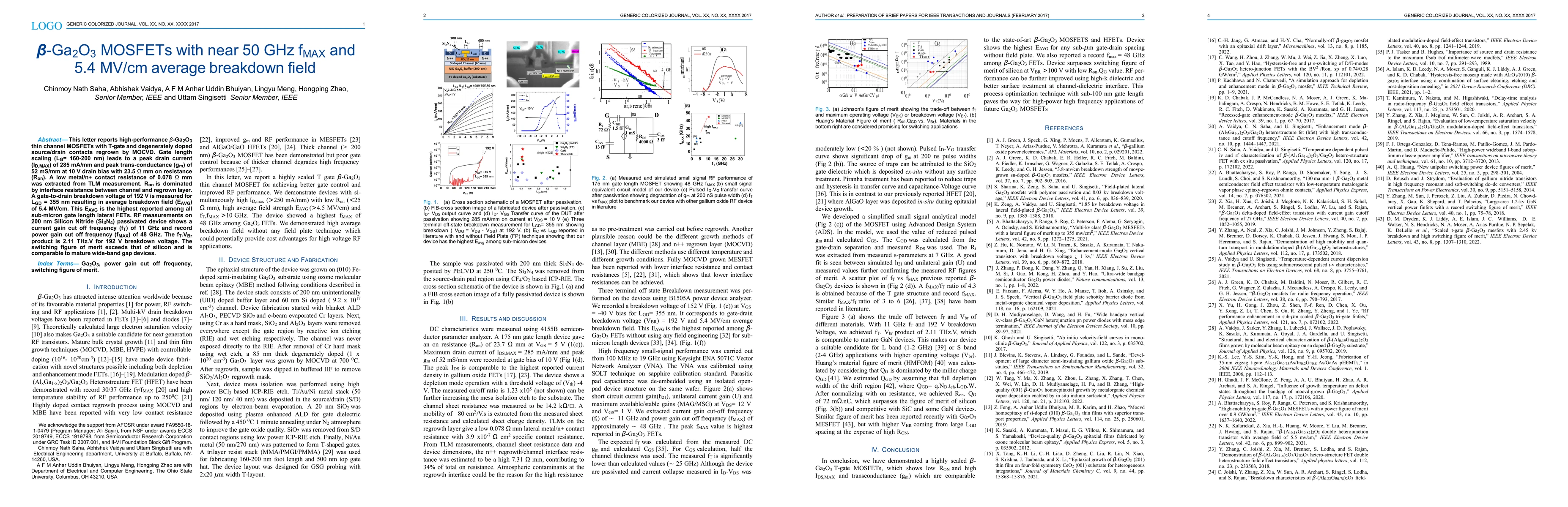
This letter reports high-performance $\mathrm{\beta} Ga2O3 thin channel MOSFETs with T-gate and degenerately doped source/drain contacts regrown by MOCVD. Gate length scaling (LG= 160-200 nm) leads ...
Epitaxial growth of \k{appa}-phase Ga2O3 thin films are investigated on c-plane sapphire, GaN- and AlNon-sapphire, and (100) oriented yttria stabilized zirconia (YSZ) substrates via metalorganic che...
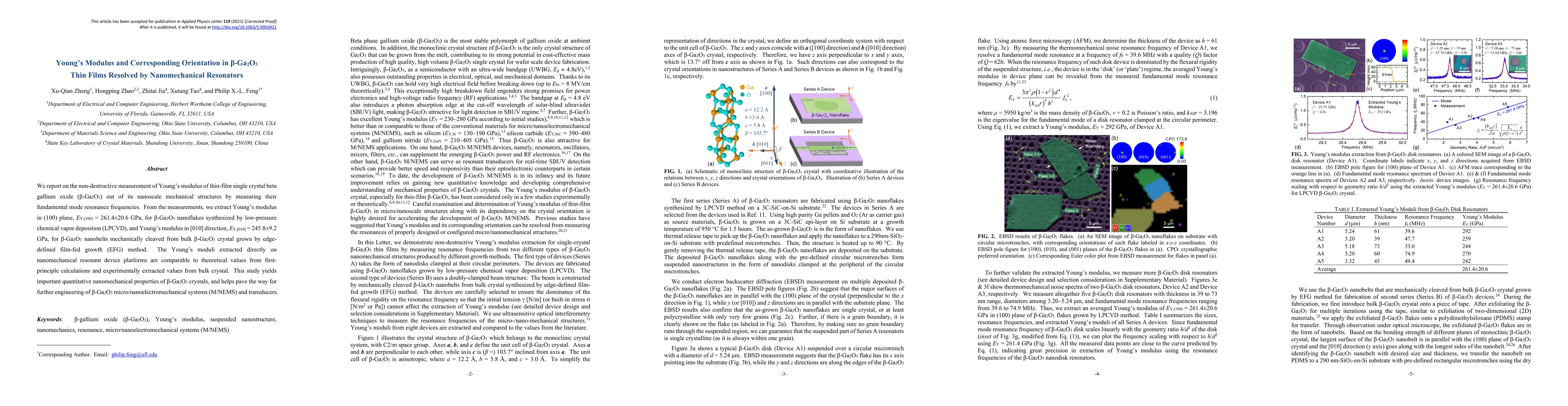
We report on the non-destructive measurement of Young's modulus of thin-film single crystal beta gallium oxide (beta-Ga2O3) out of its nanoscale mechanical structures by measuring their fundamental ...
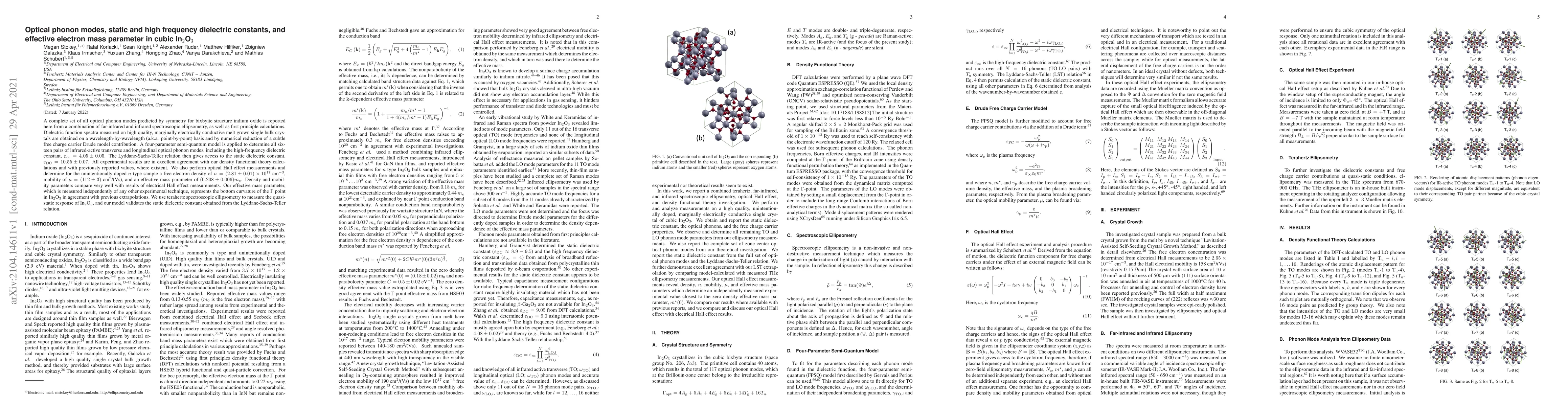
A complete set of all optical phonon modes predicted by symmetry for bixbyite structure indium oxide is reported here from a combination of far-infrared and infrared spectroscopic ellipsometry, as w...
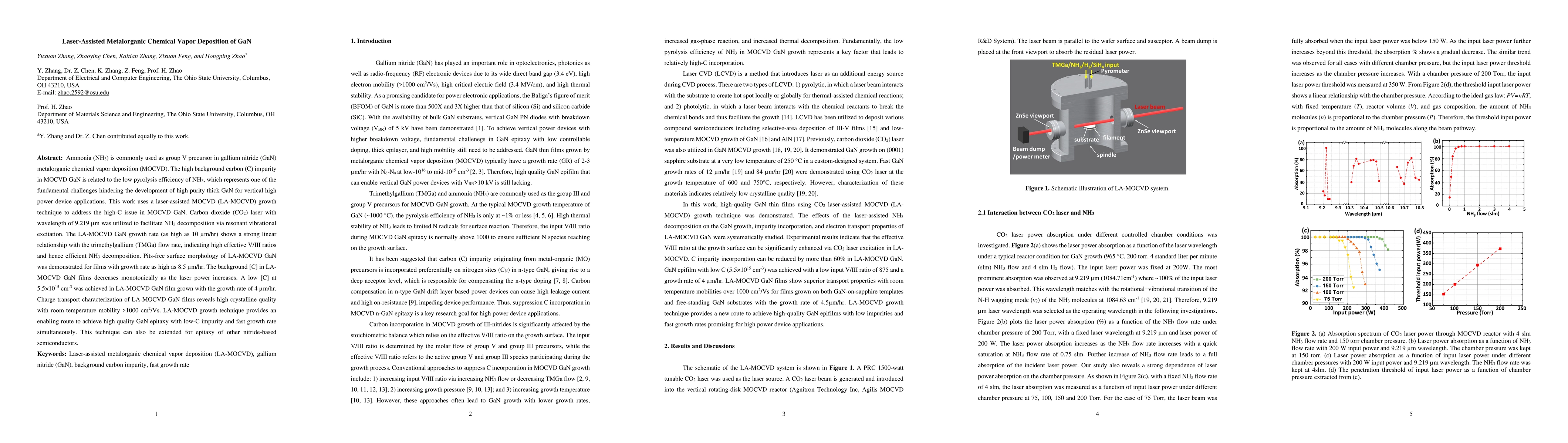
Ammonia (NH3) is commonly used as group V precursor in gallium nitride (GaN) metalorganic chemical vapor deposition (MOCVD). The high background carbon (C) impurity in MOCVD GaN is related to the lo...
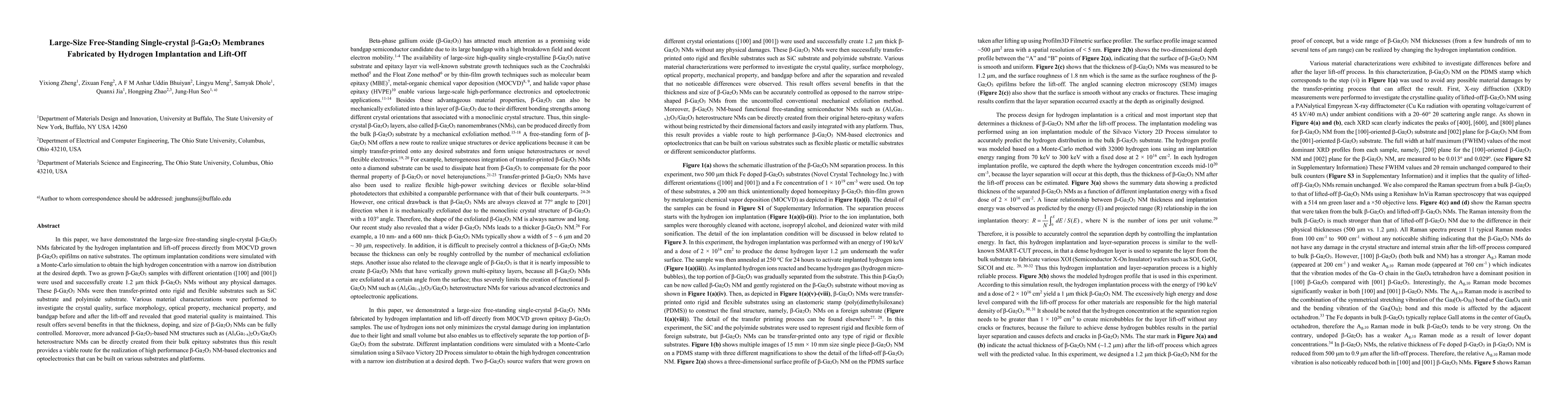
In this paper, we have demonstrated the large-size free-standing single-crystal b-Ga2O3 NMs fabricated by the hydrogen implantation and lift-off process directly from MOCVD grown b-Ga2O3 epifilms on...
A predicted type-II staggered band alignment with an approximately $1.4 eV$ valence band offset at the $ZnGeN_2/GaN$ heterointerface has inspired novel band-engineered $III-N/ZnGeN_2$ heterostructur...
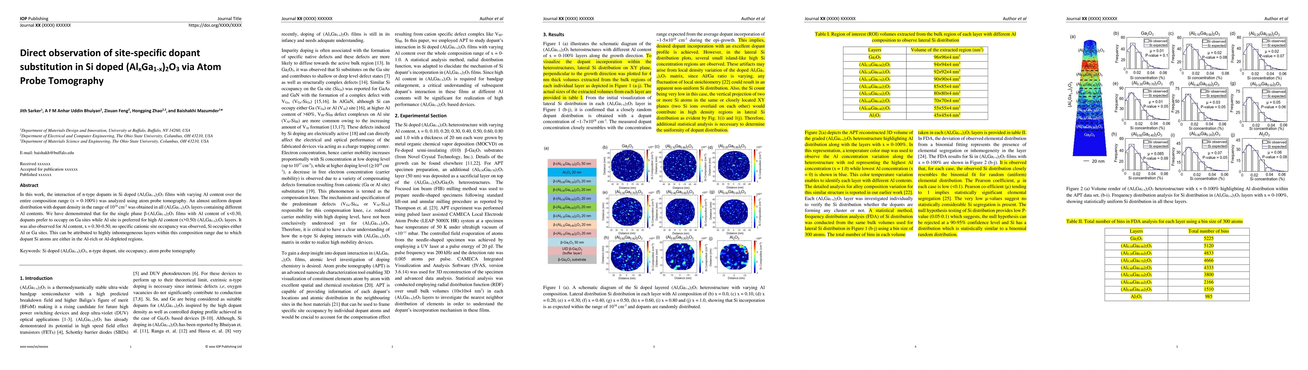
In this work, the interaction of n-type dopants in Si doped (AlxGa1-x)2O3 films with varying Al content over the entire composition range (x = 0-100%) was analyzed using atom probe tomography. An al...
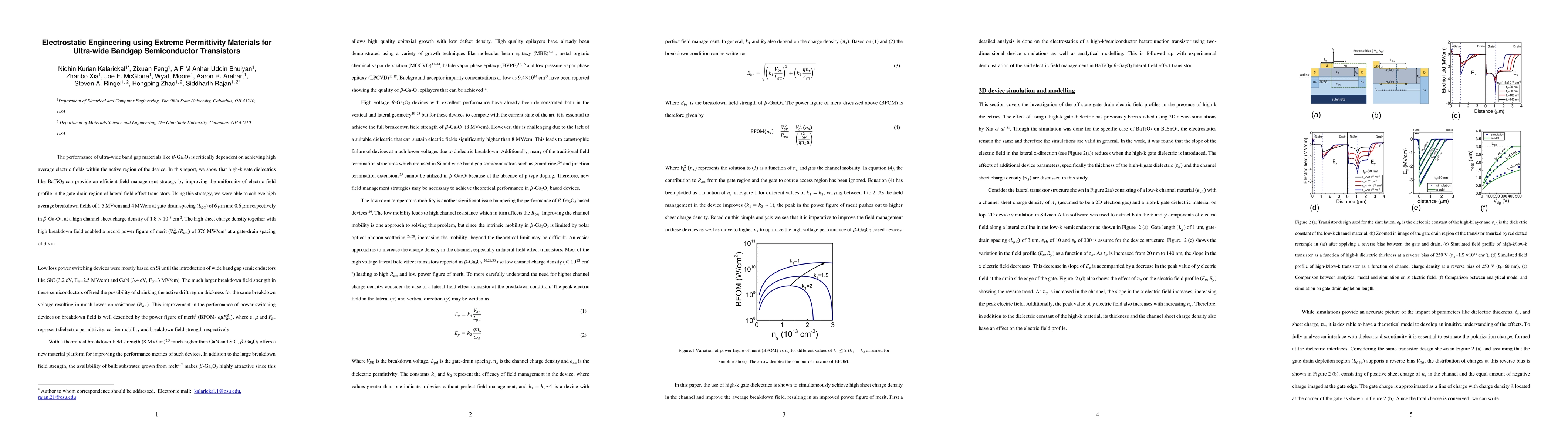
The performance of ultra-wide band gap materials like $\beta$-Ga$_\mathrm{2}$O$_\mathrm{3}$ is critically dependent on achieving high average electric fields within the active region of the device. ...
A new record-high room temperature electron Hall mobility (${\mu}_{RT} = 194\space cm^{2}/V\space s$ at $n\sim 8\times 10^{15}\space cm^{-3}$) for ${\beta}$-Ga2O3 is demonstrated in the unintentiona...
This study investigates the electrical and structural properties of MOSCAPs with in-situ MOCVD-grown Al$_2$O$_3$ dielectrics on (010) $\beta$-Ga$_2$O$_3$ and $\beta$-(Al$_x$Ga$_{1-x}$)$_2$O$_3$ films....
MgGeN2 films were synthesized using metal-organic chemical vapor deposition on GaN/c-sapphire templates and c-plane sapphire substrates. Energy-dispersive X-ray spectroscopy was used to estimate the c...
Orthorhombic-structured II-IV nitrides provide a promising opportunity to expand the material platform while maintaining compatibility with the wurtzite crystal structure of the traditional III-nitrid...
Orthorhombic II-IV nitride semiconductors offer an expanded and more tunable material set with unique properties, while maintaining close compatibility with the wurtzite crystal structure of the III-n...
AlScN thin films were grown via metalorganic chemical vapor deposition (MOCVD), showing controllable incorporation of scandium (Sc) into the AlN lattices. Systematic variation of growth parameters dem...
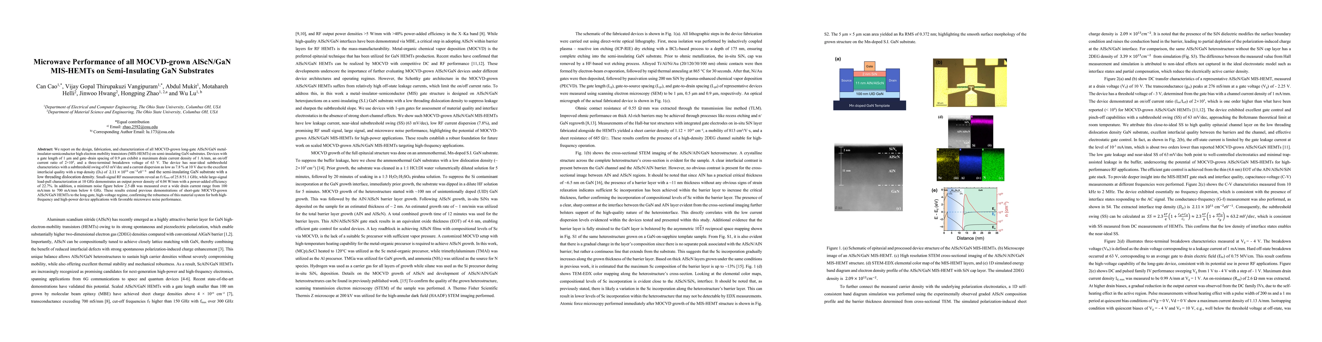
We report on the design, fabrication, and characterization of all MOCVD-grown long-gate AlScN/GaN metal-insulator-semiconductor high electron mobility transistors (MIS-HEMTs) on semi-insulating GaN su...
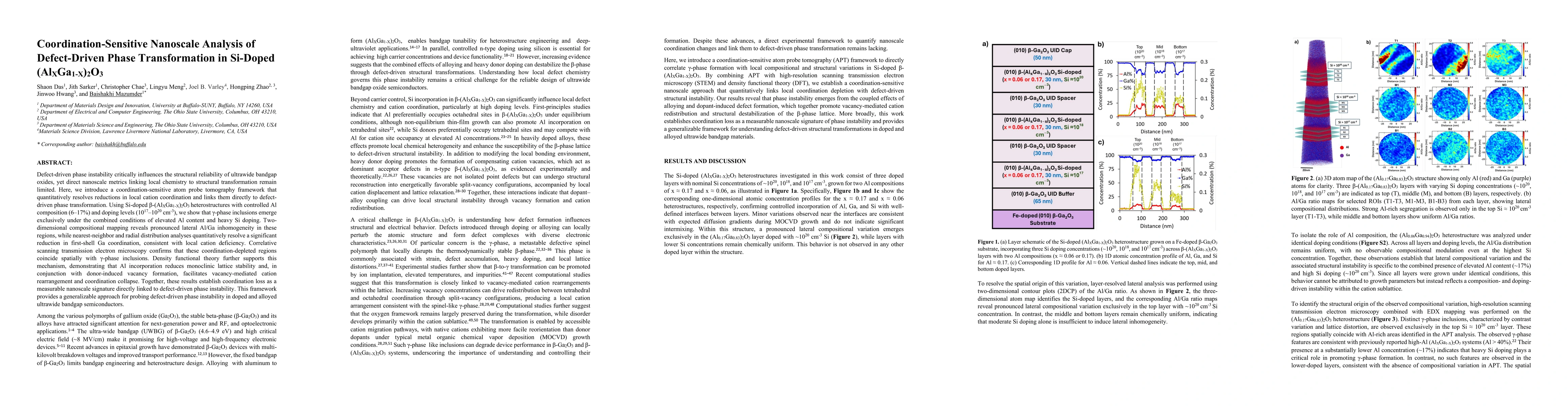
Defect-driven phase instability critically influences the structural reliability of ultrawide bandgap oxides, yet direct nanoscale metrics linking local chemistry to structural transformation remain l...