Academic Profile
Statistics
Similar Authors
Papers on arXiv
Colloidal self-assembly allows rational design of structures on the micrometer and submicrometer scale. One architecture that can generate complete 3D photonic band gaps is the diamond cubic lattice...
Antiferromagnets are promising materials for future opto-spintronic applications since they show spin dynamics in the THz range and no net magnetization. Recently, layered van der Waals (vdW) antife...
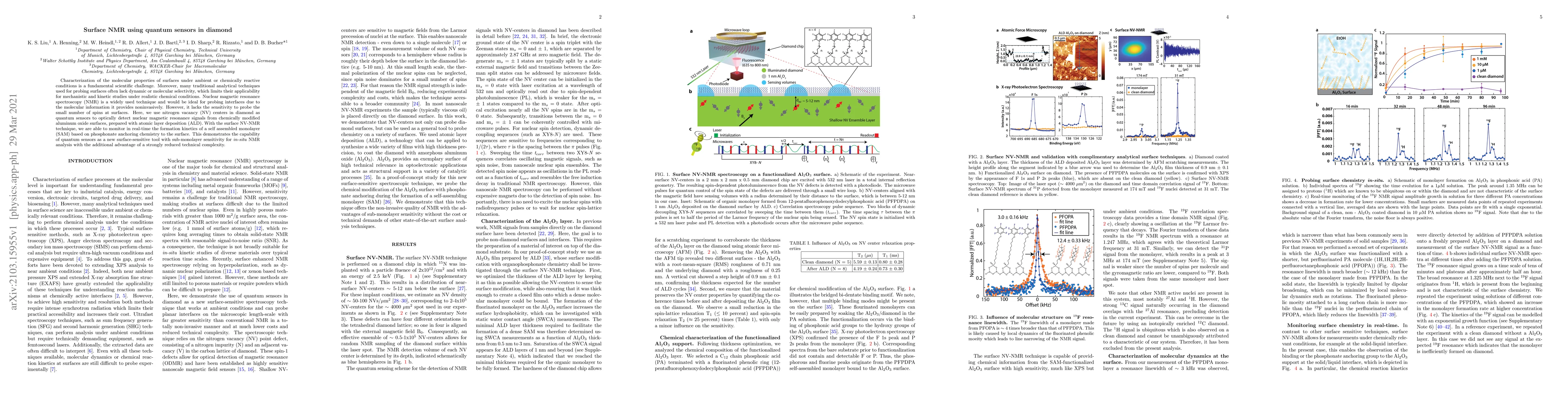
Atomic-scale magnetic field sensors based on nitrogen vacancy (NV) defects in diamonds are an exciting platform for nanoscale nuclear magnetic resonance (NMR) spectroscopy. The detection of NMR sign...
Atomic layer deposition (ALD) is a key technique for the continued scaling of semiconductor devices, which increasingly relies on reproducible and scalable processes for interface manipulation of 3D...
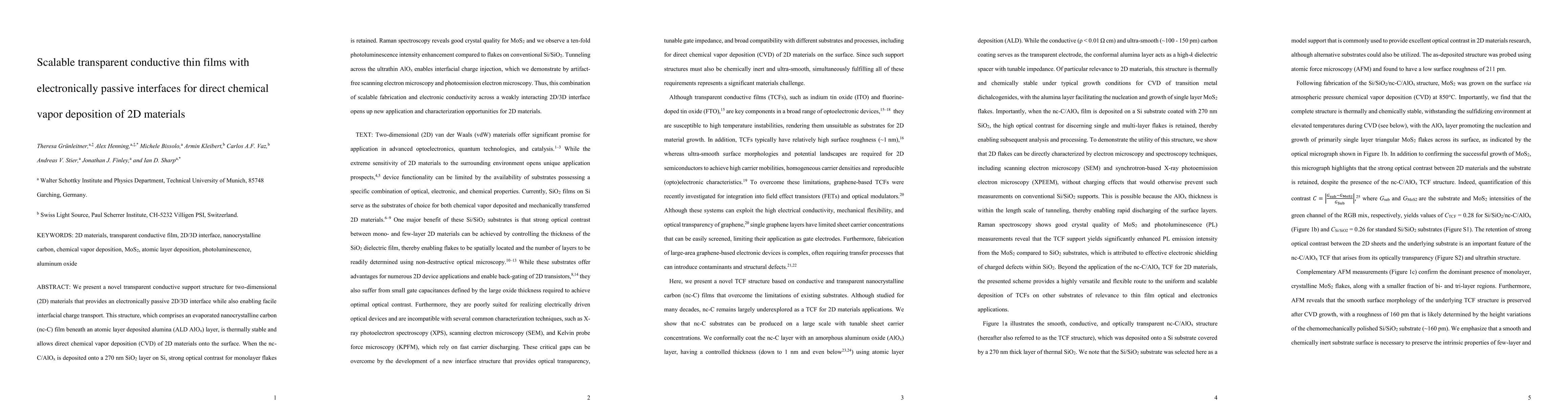
We present a novel transparent conductive support structure for two-dimensional (2D) materials that provides an electronically passive 2D/3D interface while also enabling facile interfacial charge t...
Characterization of the molecular properties of surfaces under ambient or chemically reactive conditions is a fundamental scientific challenge. Moreover, many traditional analytical techniques used ...
Atomic layer deposition (ALD) is an essential tool in semiconductor device fabrication that allows the growth of ultrathin and conformal films to precisely form heterostructures and tune interface p...
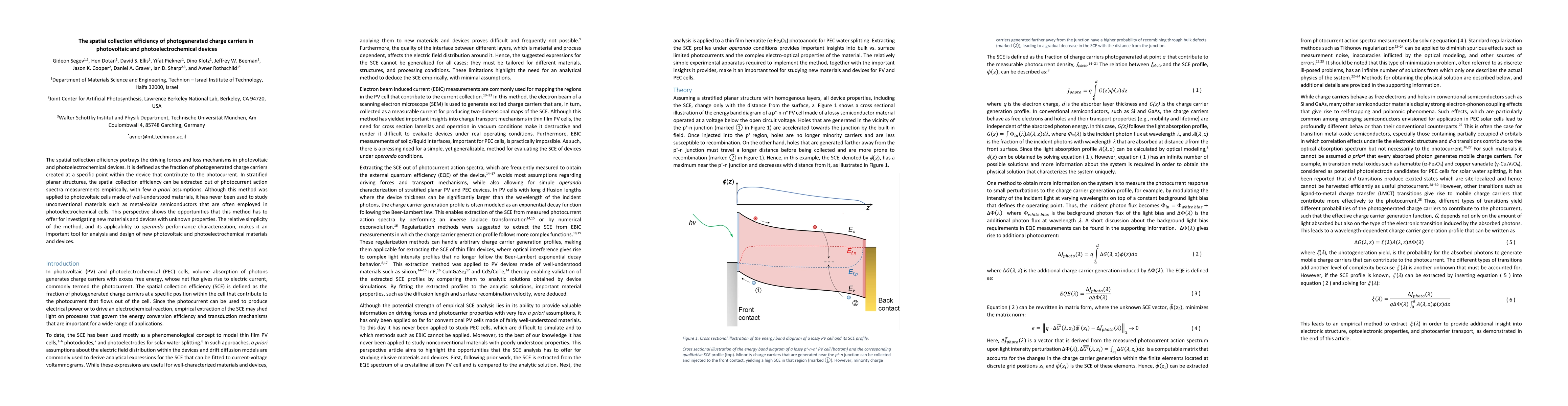
The spatial collection efficiency portrays the driving forces and loss mechanisms in photovoltaic and photoelectrochemical devices. It is defined as the fraction of photogenerated charge carriers cr...
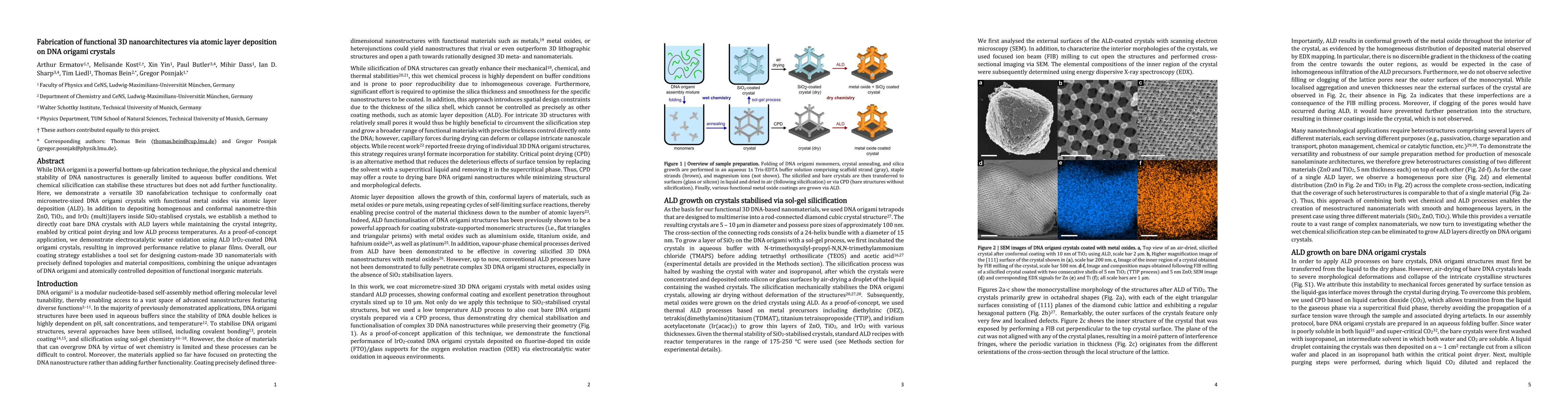
While DNA origami is a powerful bottom-up fabrication technique, the physical and chemical stability of DNA nanostructures is generally limited to aqueous buffer conditions. Wet chemical silicificatio...
Combining a precise sputter etching method with subsequent AlO$_x$ growth within an atomic layer deposition chamber enables fabrication of atomically flat lateral patterns of SiO$_2$ and AlO$_x$. The ...
InAs semiconductor quantum dots (QDs) emitting in the near infrared are promising platforms for on-demand single-photon sources and spin-photon interfaces. However, the realization of quantum-photonic...
Ternary compounds obtained by alloying wurtzite AlN with transition metals have emerged as promising materials with significantly enhanced piezoelectric characteristics relative to binary AlN. The inc...
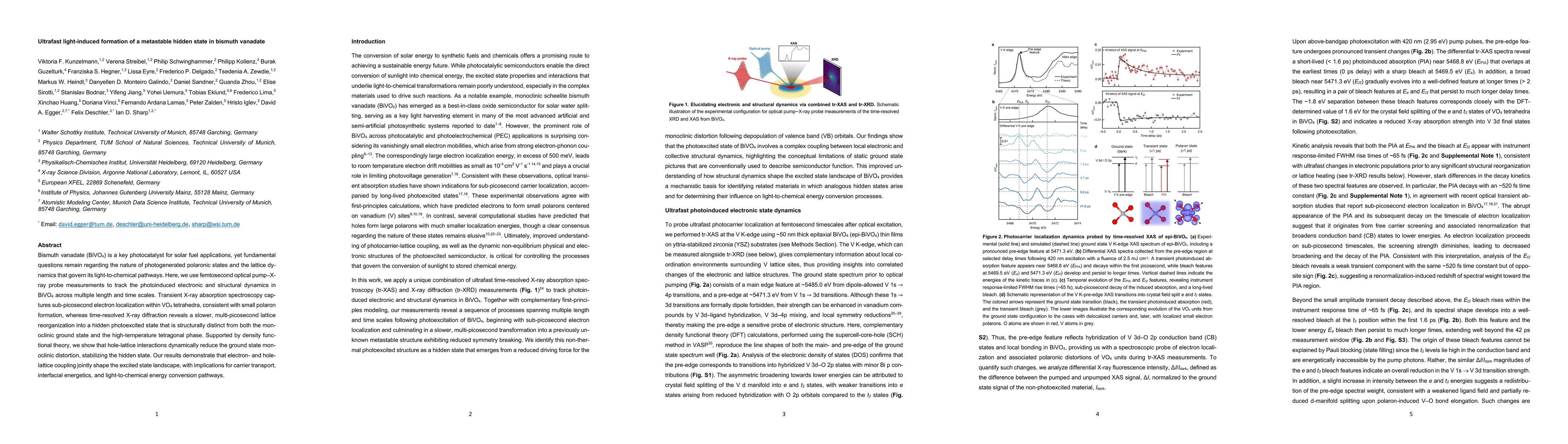
Bismuth vanadate (BiVO$_4$) is a key photocatalyst for solar fuel applications, yet fundamental questions remain regarding the nature of photogenerated polaronic states and the lattice dynamics that g...
Ta$_{3}$N$_{5}$ is among the most intensively studied photoanode materials for solar-driven water oxidation, yet its performance often remains limited by short carrier lifetimes and defect mediated re...
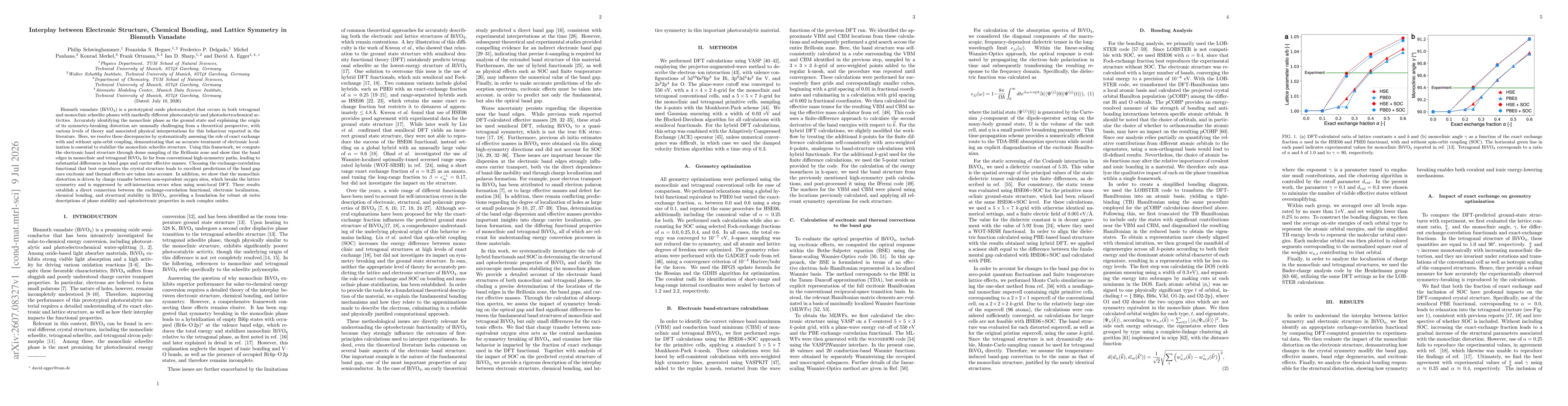
Bismuth vanadate (BiVO$_4$) is a prototypical oxide photocatalyst that occurs in both tetragonal and monoclinic scheelite phases with markedly different photocatalytic and photoelectrochemical activit...