ArxivLens
I
Researcher

Ilaria Zardo

17 papers on arXiv

17 arXiv Papers
71 Total Publications
Profile

Academic Profile

Name I. Zardo
Total Papers 71
Scholar Profile View on Semantic Scholar
Metrics

Statistics

17 arXiv Papers
71 Total Publications
Publications

Papers on arXiv

Thumbnail for High quality CVD deposition of Ge layers for Ge/SiGe Quantum Well
  heterostructures
arXiv
High quality CVD deposition of Ge layers for Ge/SiGe Quantum Well heterostructures

A great deal of interest is directed nowadays towards the development of innovative technologies in the field of quantum information and quantum computing, with emphasis on obtaining reliable qubits...

Thumbnail for GaAs/GaP Superlattice Nanowires for Tailoring Phononic Properties at the
  Nanoscale: Implications for Thermal Engineering
arXiv
GaAs/GaP Superlattice Nanowires for Tailoring Phononic Properties at the Nanoscale: Implications for Thermal Engineering

The possibility to tune the functional properties of nanomaterials is key to their technological applications. Superlattices, i.e., periodic repetitions of two or more materials in different dimensi...

Thumbnail for In-plane thermal diffusivity determination using beam-offset
  frequency-domain thermoreflectance with a one-dimensional optical heat source
arXiv
In-plane thermal diffusivity determination using beam-offset frequency-domain thermoreflectance with a one-dimensional optical heat source

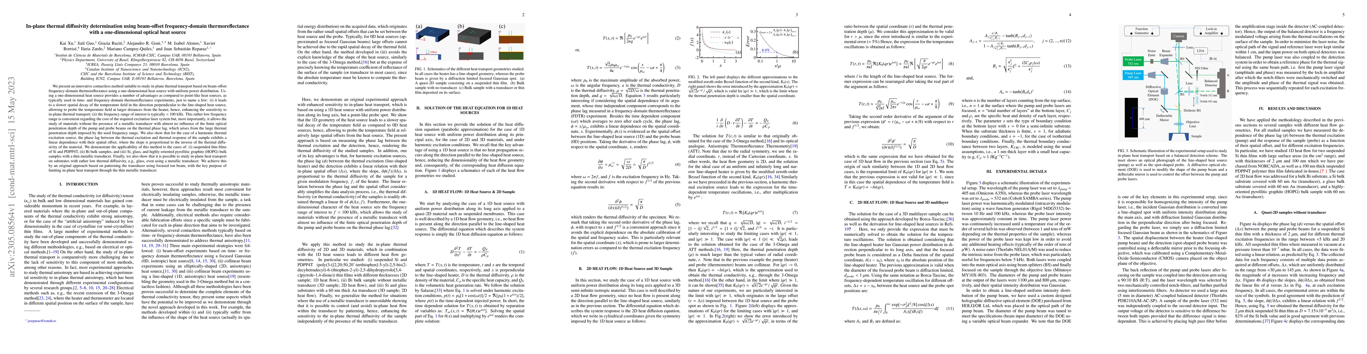
We present an innovative contactless method suitable to study in-plane thermal transport based on beam-offset frequency-domain thermoreflectance using a one-dimensional heat source with uniform powe...

Thumbnail for Phonon transport across twin boundaries and twin superlattices
arXiv
Phonon transport across twin boundaries and twin superlattices

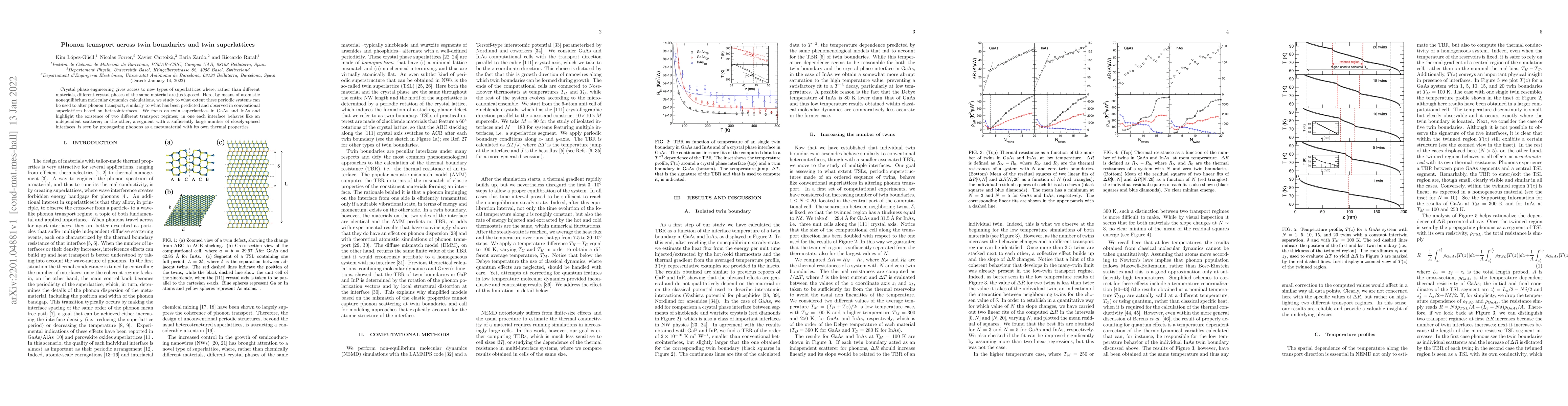
Crystal phase engineering gives access to new types of superlattices where, rather than different materials, different crystal phases of the same material are juxtaposed. Here, by means of atomistic...

Thumbnail for Probing Lattice Dynamics and Electronic Resonances in Hexagonal Ge and
  SixGe1-x Alloys in Nanowires by Raman Spectroscopy
arXiv
Probing Lattice Dynamics and Electronic Resonances in Hexagonal Ge and SixGe1-x Alloys in Nanowires by Raman Spectroscopy

Recent advances in nanowire synthesis have enabled the realization of crystal phases that in bulk are attainable only under extreme conditions, i.e. high temperature and/or high pressure. For group ...

Thumbnail for Nanowires for heat conversion
arXiv
Nanowires for heat conversion

This review focuses on the investigation and enhancement of the thermoelectric properties of semiconducting nanowires (NWs). NWs are nanostructures with typical diameters between few to hundreds of ...

Thumbnail for Experimental demonstration of the suppression of optical phonon
  splitting in 2D materials by Raman spectroscopy
arXiv
Experimental demonstration of the suppression of optical phonon splitting in 2D materials by Raman spectroscopy

Raman spectroscopy is one of the most extended experimental techniques to investigate thin-layered 2D materials. For a complete understanding and modeling of the Raman spectrum of a novel 2D materia...

Thumbnail for New insights in the lattice dynamics of monolayers, bilayers, and
  trilayers of WSe2 and unambiguous determination of few-layer-flakes'
  thickness
arXiv
New insights in the lattice dynamics of monolayers, bilayers, and trilayers of WSe2 and unambiguous determination of few-layer-flakes' thickness

Among the most common few-layers transition metal dichalcogenides (TMDs), WSe2 is the most challenging material from the lattice dynamics point of view. Indeed, for a long time the main two phonon m...

Thumbnail for Impact of surface treatments on the transport properties of germanium
  2DHGs
arXiv
Impact of surface treatments on the transport properties of germanium 2DHGs

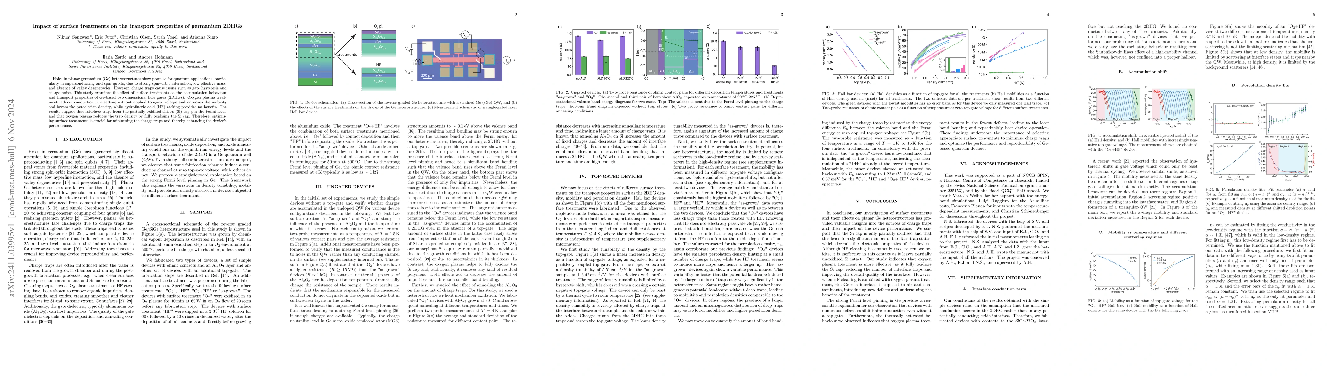
Holes in planar germanium (Ge) heterostructures show promise for quantum applications, particularly in superconducting and spin qubits, due to strong spin-orbit interaction, low effective mass, and ab...

Thumbnail for A backgate for enhanced tunability of holes in planar germanium
arXiv
A backgate for enhanced tunability of holes in planar germanium

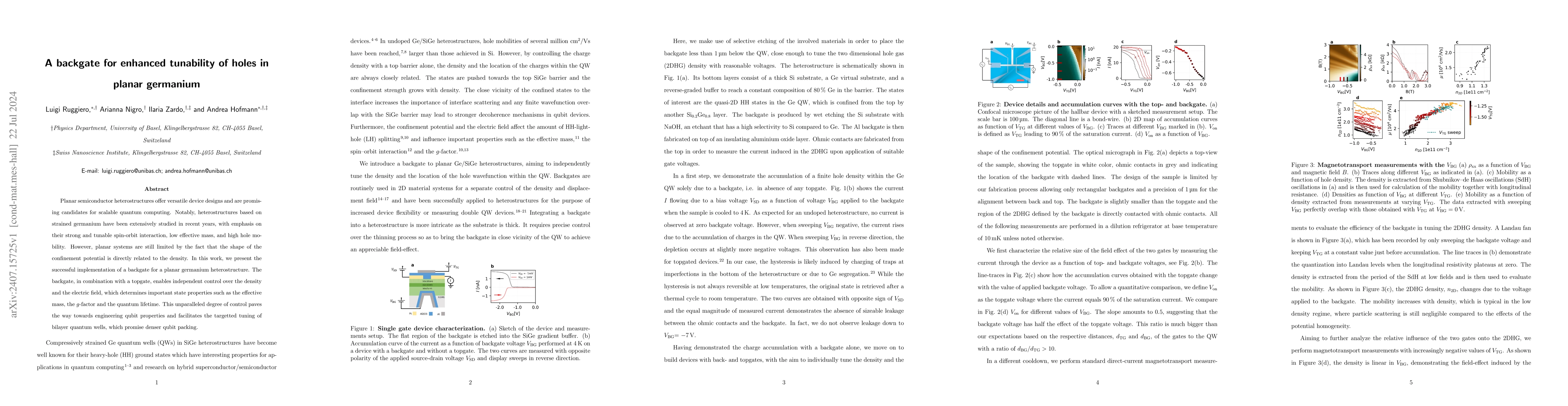
Planar semiconductor heterostructures offer versatile device designs and are promising candidates for scalable quantum computing. Notably, heterostructures based on strained germanium have been extens...

Thumbnail for Phonon interference effects in GaAs-GaP superlattice nanowires
arXiv
Phonon interference effects in GaAs-GaP superlattice nanowires

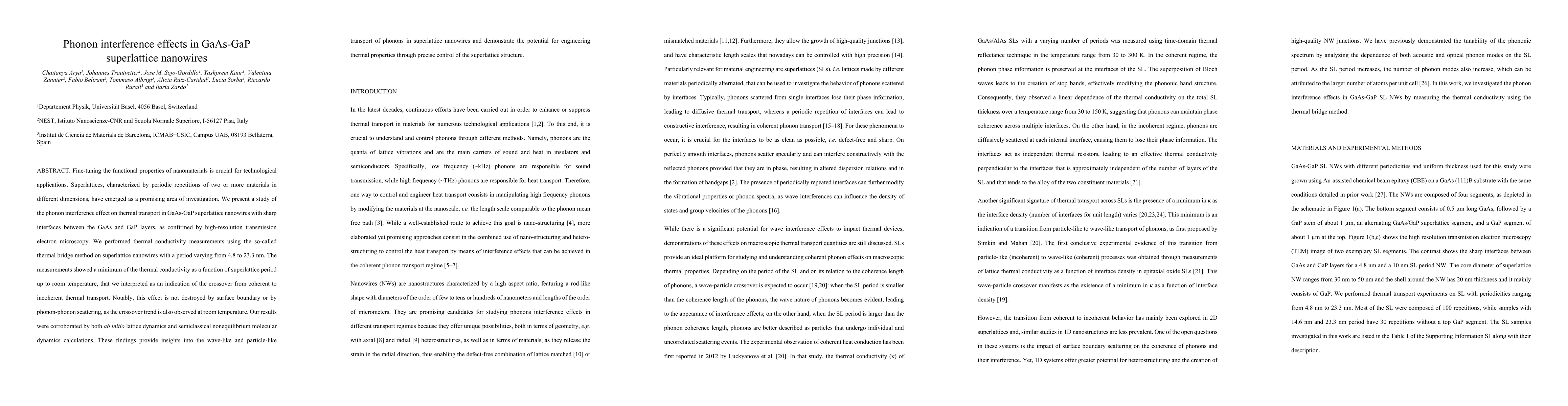
Fine-tuning the functional properties of nanomaterials is crucial for technological applications. Superlattices, characterized by periodic repetitions of two or more materials in different dimensions,...

Thumbnail for Unraveling energy flow mechanisms in semiconductors by ultrafast
  spectroscopy: Germanium as a case study
arXiv
Unraveling energy flow mechanisms in semiconductors by ultrafast spectroscopy: Germanium as a case study

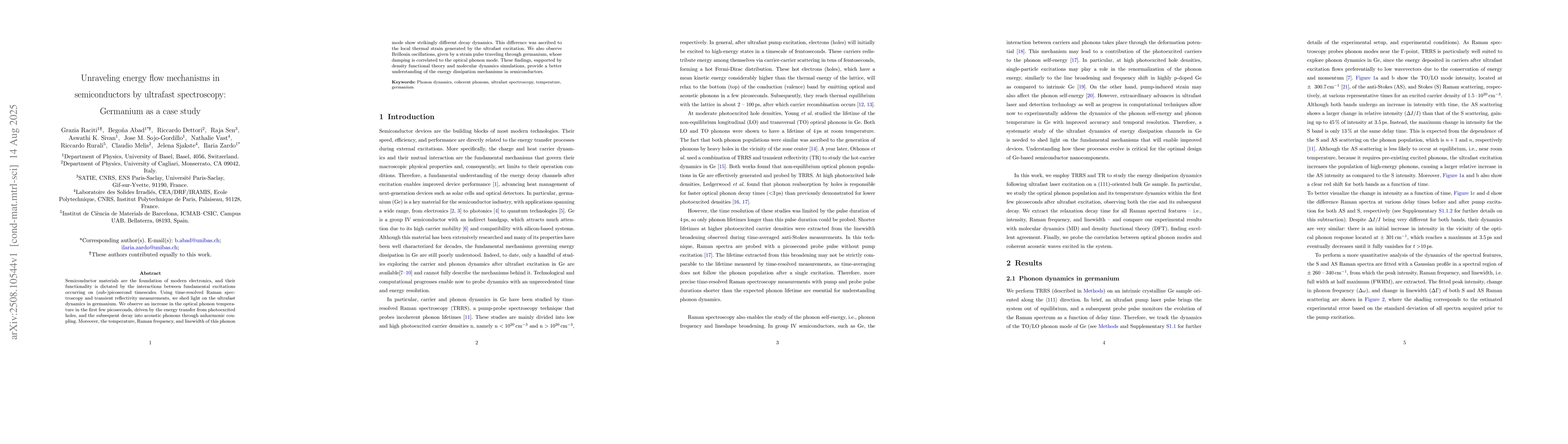
Semiconductor materials are the foundation of modern electronics, and their functionality is dictated by the interactions between fundamental excitations occurring on (sub-)picosecond timescales. Usin...

Thumbnail for Bandgap Engineering On Demand in GaAsN Nanowires by Post-Growth HydrogennImplantation
arXiv
Bandgap Engineering On Demand in GaAsN Nanowires by Post-Growth HydrogennImplantation

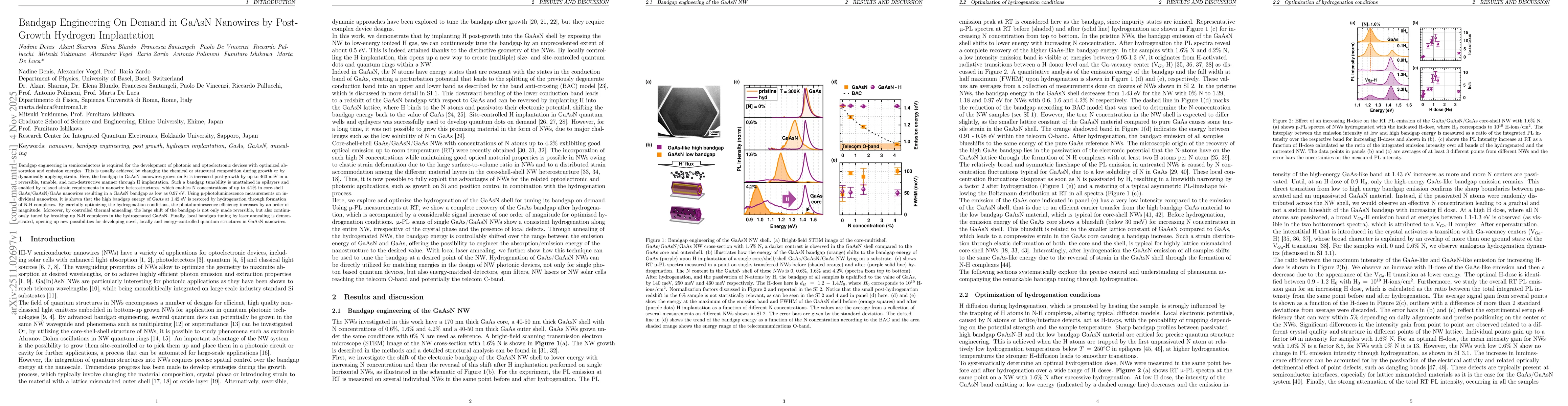
Bandgap engineering in semiconductors is required for the development of photonic and optoelectronic devices with optimized absorption and emission energies. This is usually achieved by changing the c...

Thumbnail for Low-loss frequency-tunable Josephson junction array cavities on Ge/SiGe heterostructures with a tapered etching approach
arXiv
Low-loss frequency-tunable Josephson junction array cavities on Ge/SiGe heterostructures with a tapered etching approach

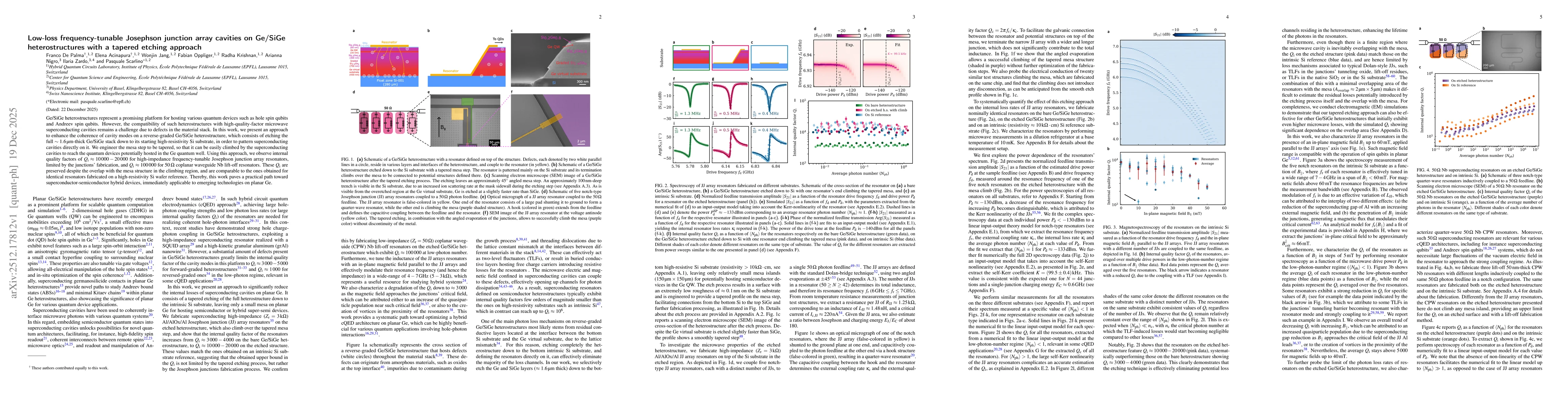
Ge/SiGe heterostructures represent a promising platform for hosting various quantum devices such as hole spin qubits and Andreev spin qubits. However, the compatibility of such heterostructures with h...

Thumbnail for Quantifying Strain and its Effect on Charge Transport in Ge/Si Core/Shell Nanowires
arXiv
Quantifying Strain and its Effect on Charge Transport in Ge/Si Core/Shell Nanowires

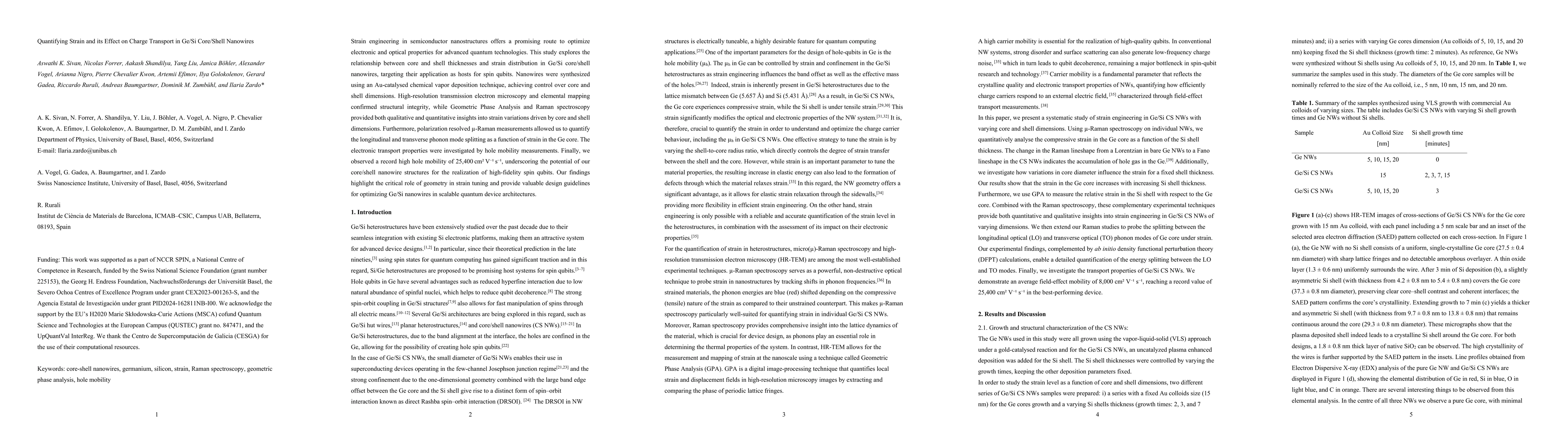
Strain engineering in semiconductor nanostructures offers a promising route to optimize electronic and optical properties for advanced quantum technologies. This study explores the relationship betwee...

Thumbnail for Direct observation of strain and confinement shaping the hole subbands of Ge quantum wells
arXiv
Direct observation of strain and confinement shaping the hole subbands of Ge quantum wells

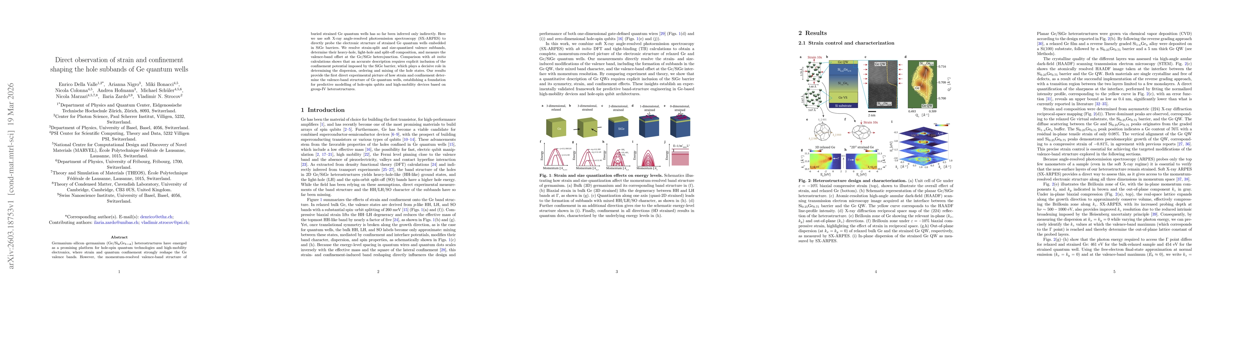
Germanium-silicon-germanium (Ge/Si$_{x}$Ge$_{1-x}$) heterostructures have emerged as a promising platform for hole-spin quantum technologies and high-mobility electronics, where strain and quantum con...

Thumbnail for Thermal conductivity tuning of scalable nanopatterned silicon membranes measured with a three-probe method
arXiv
Thermal conductivity tuning of scalable nanopatterned silicon membranes measured with a three-probe method

Phononic silicon structures have emerged as an integrable and scalable nanosystem for tailoring thermal transport. However, their widespread adoption has been limited by their complex fabrication path...

This website uses cookies to ensure you get the best experience. Learn more