ArxivLens
I
Researcher

Ioannis Deretzis

9 papers on arXiv

9 arXiv Papers
162 Total Publications
Profile

Academic Profile

Name I. Deretzis
Total Papers 162
Scholar Profile View on Semantic Scholar
Metrics

Statistics

9 arXiv Papers
162 Total Publications
Publications

Papers on arXiv

Thumbnail for Laser Annealed SiO2/Si1-xGex Scaffolds for Nanoscaled Devices, Synergy
  of Experiment and Computation
arXiv
Laser Annealed SiO2/Si1-xGex Scaffolds for Nanoscaled Devices, Synergy of Experiment and Computation

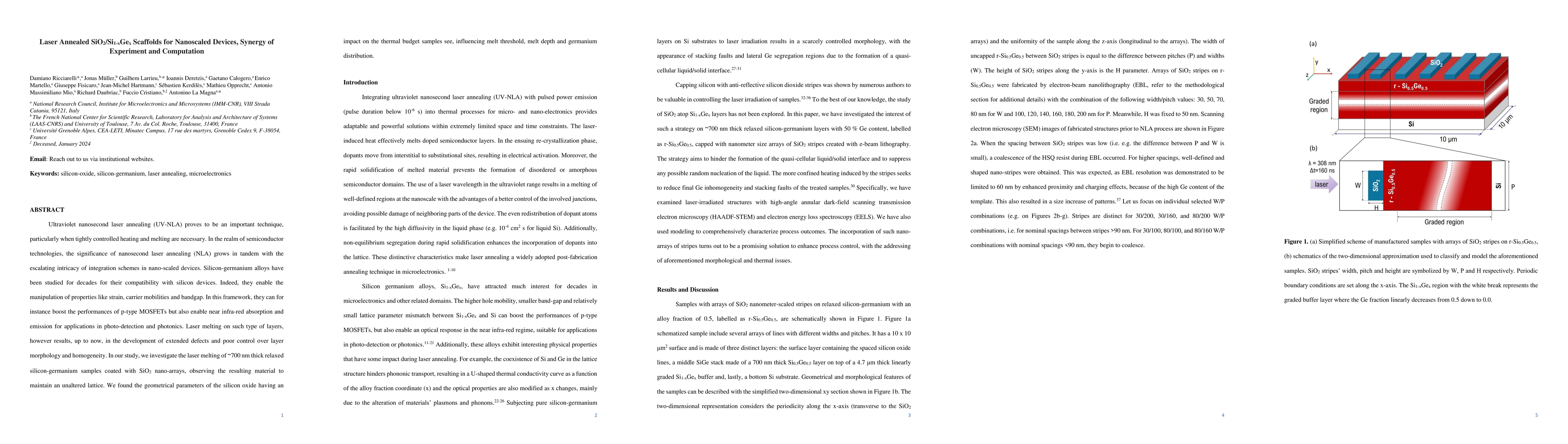
Ultraviolet nanosecond laser annealing (UV-NLA) proves to be an important technique, particularly when tightly controlled heating and melting are necessary. In the realm of semiconductor technologie...

Thumbnail for Local Coordination Modulates the Reflectivity of Liquefied Si-Ge Alloys
arXiv
Local Coordination Modulates the Reflectivity of Liquefied Si-Ge Alloys

The properties of liquid Si-Ge binary systems at melting conditions deviate from those expected by the ideal alloy approximation. Particularly, a non-linear dependence of the dielectric functions oc...

Thumbnail for Atomistic insights into ultrafast SiGe nanoprocessing
arXiv
Atomistic insights into ultrafast SiGe nanoprocessing

Controlling ultrafast material transformations with atomic precision is essential for future nanotechnology. Pulsed laser annealing (LA), inducing extremely rapid and localized phase transitions, is...

Thumbnail for Impact of surface reflectivity on the ultra-fast laser melting of
  silicon-germanium alloys
arXiv
Impact of surface reflectivity on the ultra-fast laser melting of silicon-germanium alloys

Ultraviolet nanosecond laser annealing (LA) is a powerful tool where strongly confined heating and melting are desirable. In semiconductor technologies the importance of LA increases with the increa...

Thumbnail for Comparing different solutions for testing resistive defects in low-power
  SRAMs
arXiv
Comparing different solutions for testing resistive defects in low-power SRAMs

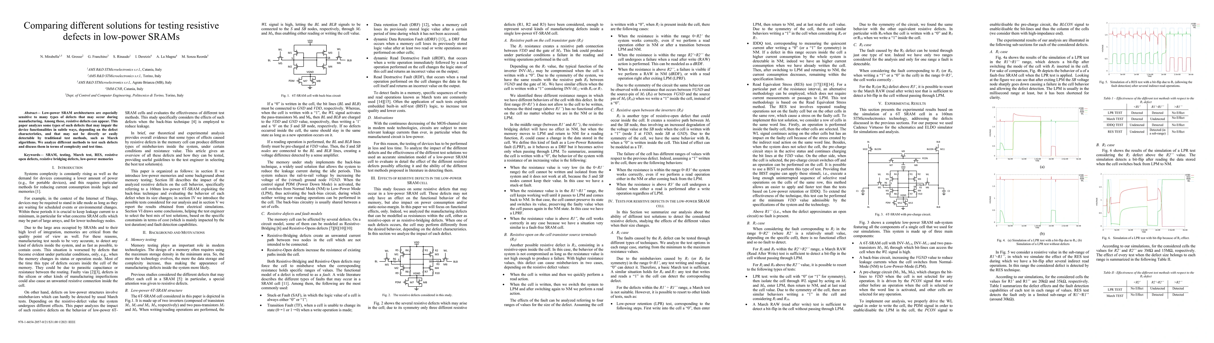
Low-power SRAM architectures are especially sensitive to many types of defects that may occur during manufacturing. Among these, resistive defects can appear. This paper analyzes some types of such ...

Thumbnail for Electron trapping at SiO2/4H-SiC interface probed by transient
  capacitance measurements and atomic resolution chemical analysis
arXiv
Electron trapping at SiO2/4H-SiC interface probed by transient capacitance measurements and atomic resolution chemical analysis

Studying the electrical and structural properties of the interface of the gate oxide (SiO2) with silicon carbide (4H-SiC) is a fundamental topic, with important implications for understanding and op...

Thumbnail for Tailoring nuclear spins order with defects: a Quantum-TCAD study
arXiv
Tailoring nuclear spins order with defects: a Quantum-TCAD study

The full design of relevant systems for quantum applications, ranging from quantum simulation to sensing, is presented using a combination of atomistic methods. A prototypical system features a two-di...

Thumbnail for First-Principles Investigation of Surface-Induced Effects on the Properties of Divacancy Qubits in 3C-SiC
arXiv
First-Principles Investigation of Surface-Induced Effects on the Properties of Divacancy Qubits in 3C-SiC

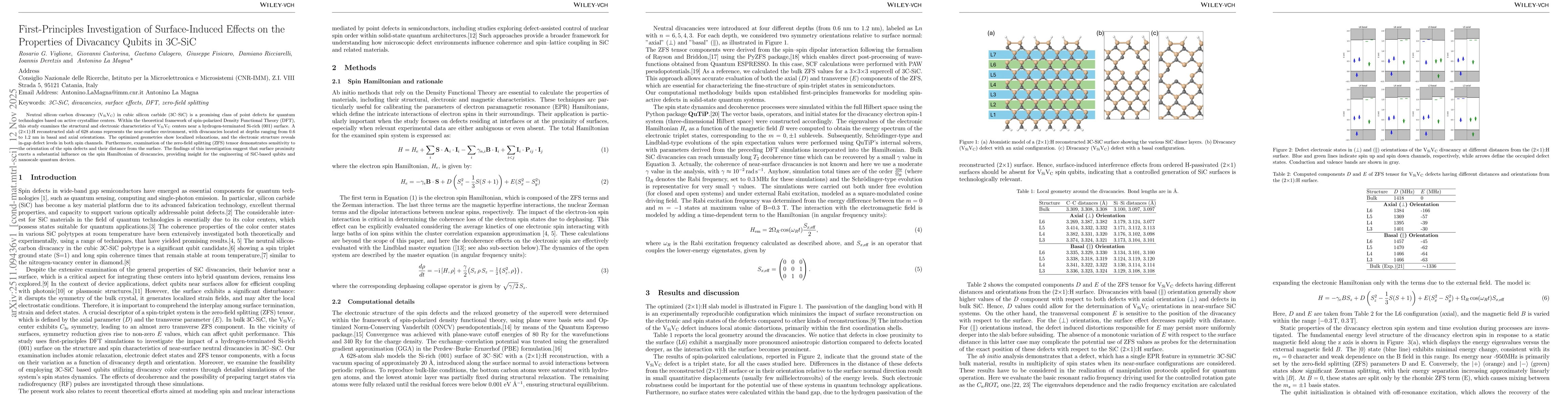
Neutral silicon-carbon divacancy (V$_{Si}$V$_{C}$) in cubic silicon carbide (3C-SiC) is a promising class of point defects for quantum technologies based on active crystalline centers. Within the theo...

Thumbnail for Molecular Dynamics Study of Defect Evolution Mechanisms in 3C-SiC for Quantum Technologies
arXiv
Molecular Dynamics Study of Defect Evolution Mechanisms in 3C-SiC for Quantum Technologies

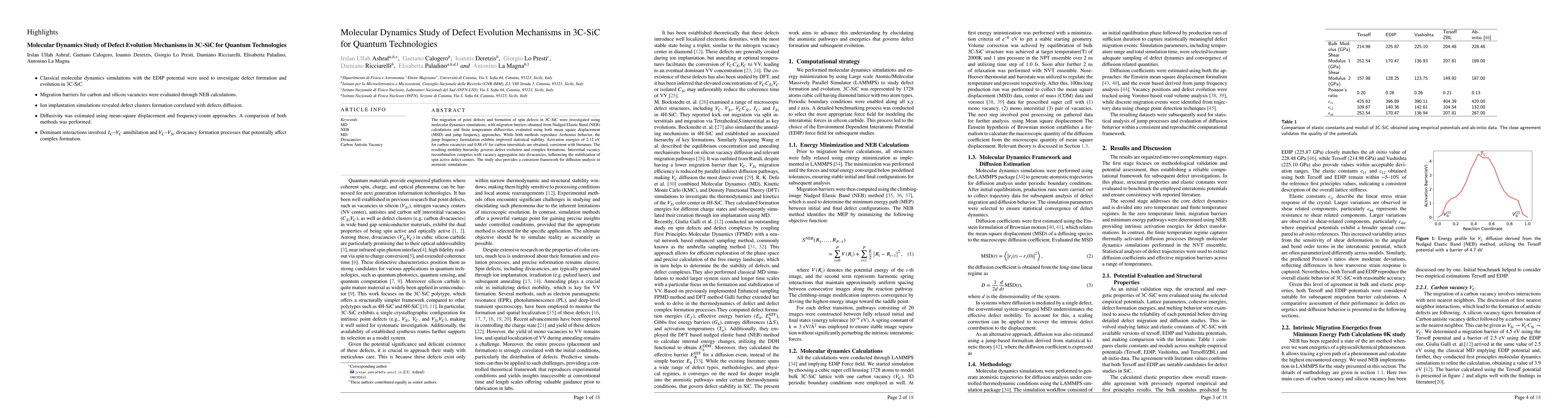
The migration of point defects and formation of spin defects in 3C-SiC were investigated using molecular dynamics simulations, with migration barriers obtained from Nudged Elastic Band (NEB) calculati...

This website uses cookies to ensure you get the best experience. Learn more