Academic Profile
Statistics
Similar Authors
Papers on arXiv
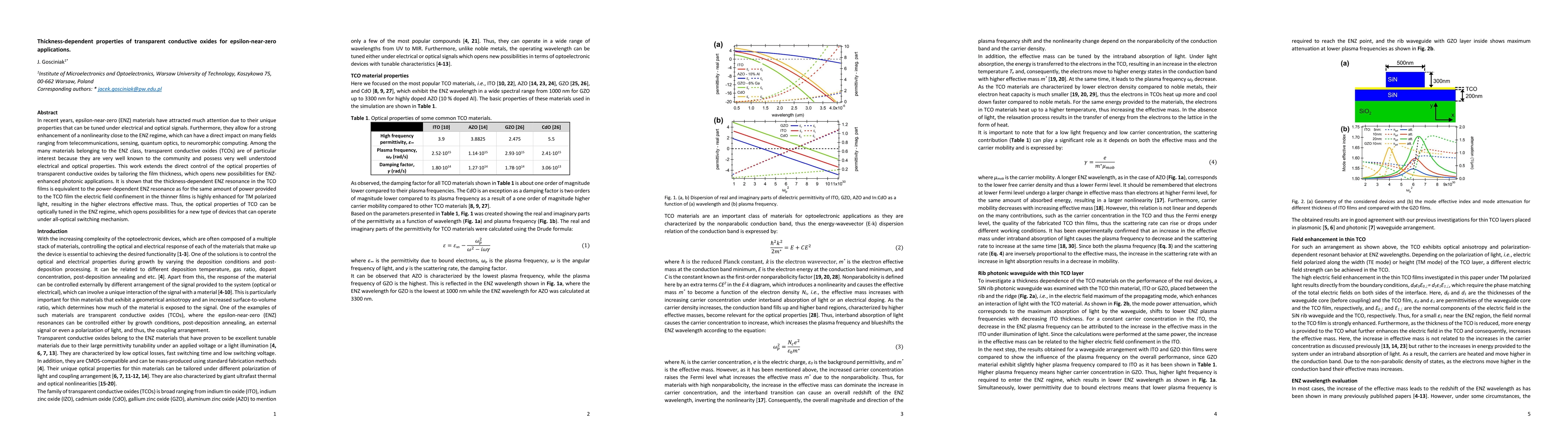
In recent years, epsilon-near-zero (ENZ) materials have attracted much attention due to their unique properties that can be tuned under electrical and optical signals. Furthermore, they allow for a ...
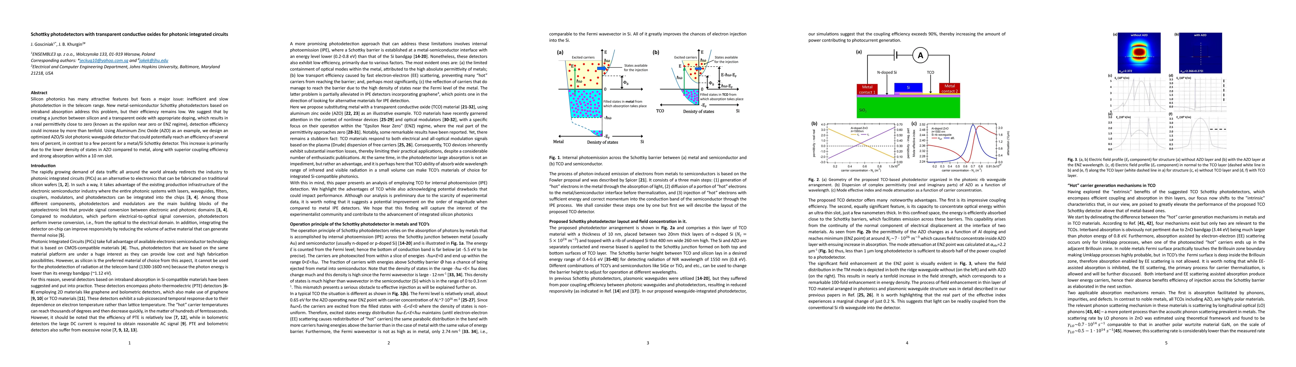
Silicon photonics has many attractive features but faces a major issue: inefficient and slow photodetection in the telecom range. New metal-semiconductor Schottky photodetectors based on intraband a...
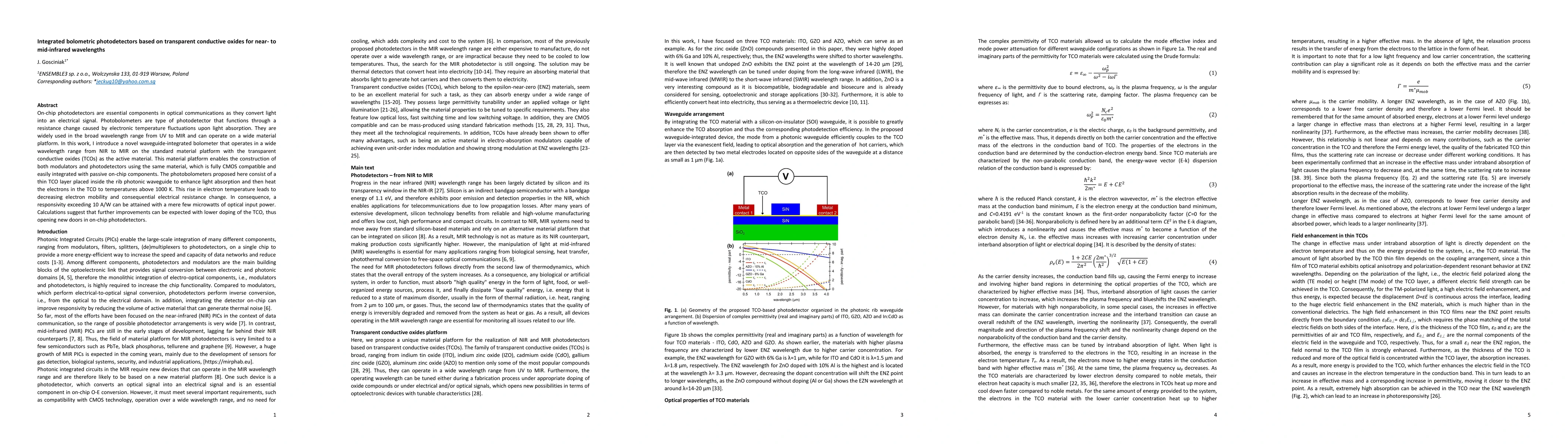
On-chip photodetectors are essential components in optical communications as they convert light into an electrical signal. Photobolometers are type of photodetector that functions through a resistan...
Fully CMOS-compatible photonic memory holding devices hold a potential in a development of ultrafast artificial neural networks. Leveraging the benefits of photonics such as high-bandwidth, low late...
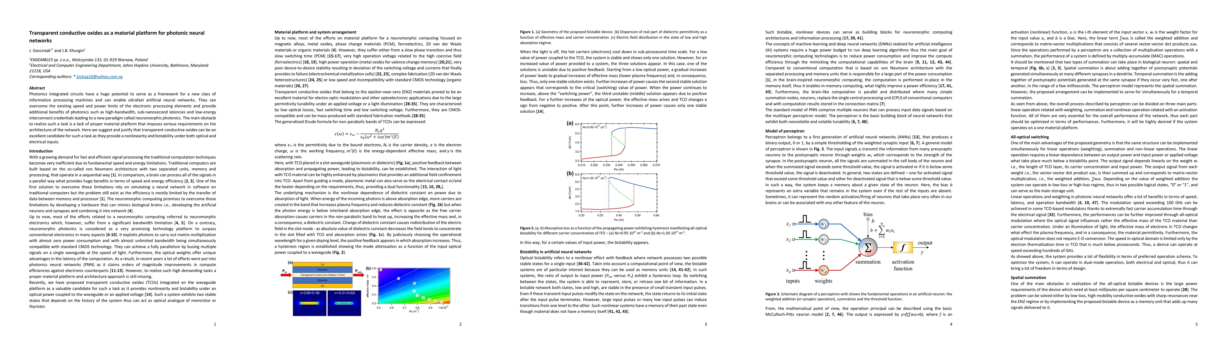
Photonics integrated circuits have a huge potential to serve as a framework for a new class of information processing machines and can enable ultrafast artificial neural networks. They can overcome ...
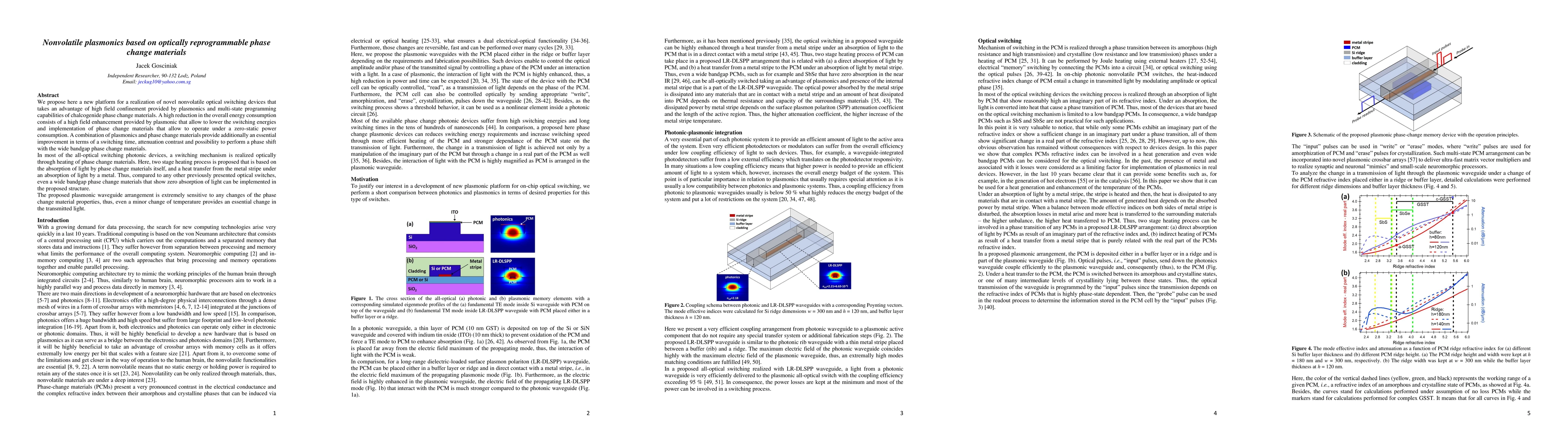
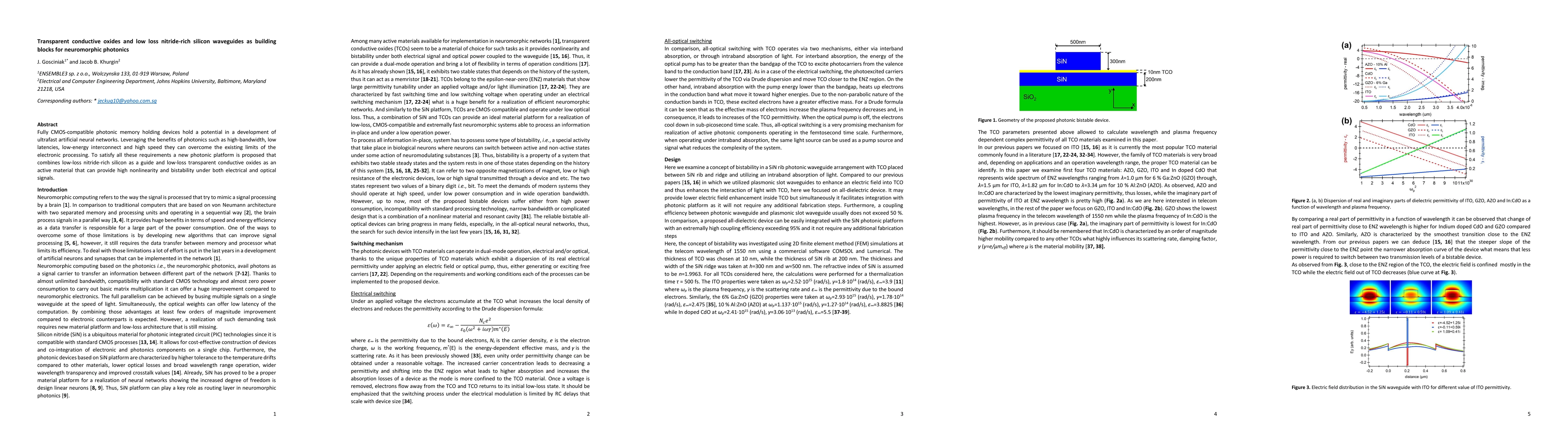
We propose here a new platform for a realization of novel nonvolatile optical switching devices that takes an advantage of high field confinement provided by plasmonics and multi-state programming c...
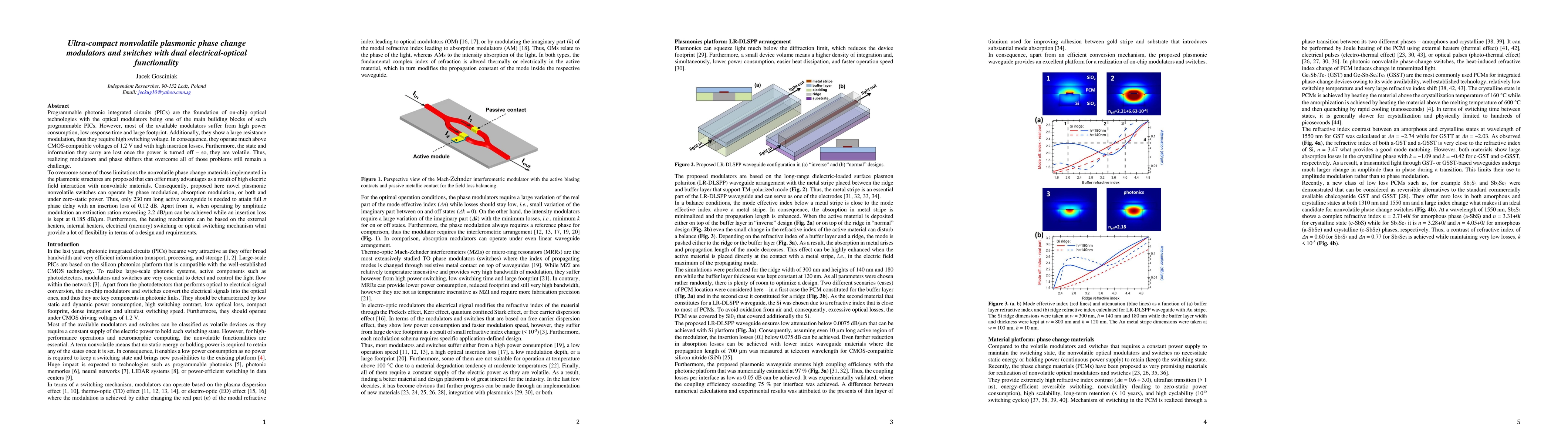
Programmable photonic integrated circuits (PICs) are the foundation of on-chip optical technologies with the optical modulators being one of the main building blocks of such programmable PICs. Howev...
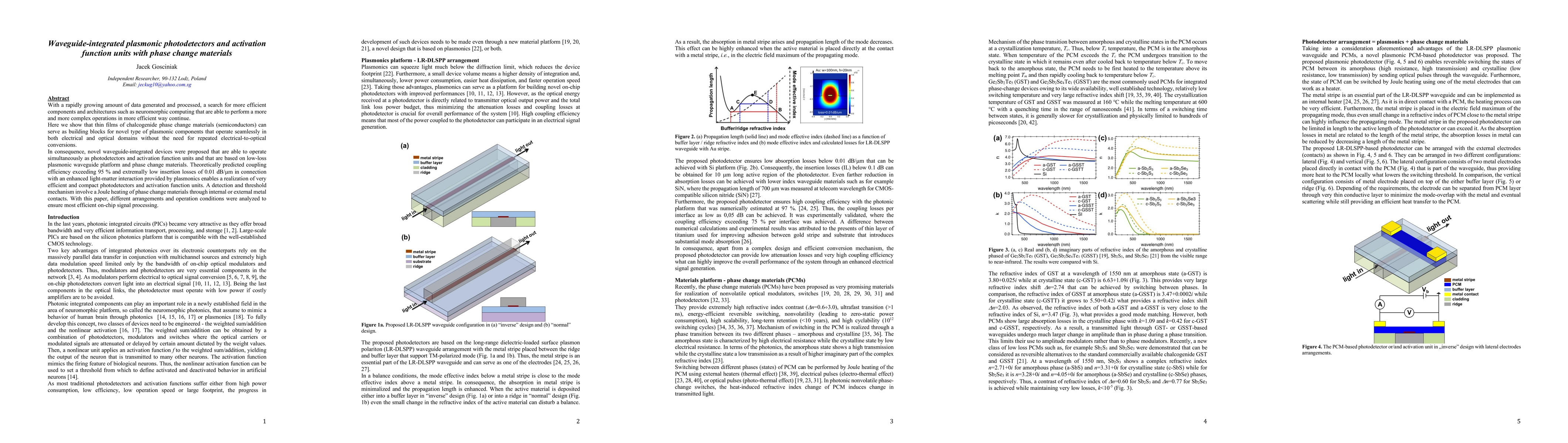
With a rapidly growing amount of data generated and processed, a search for more efficient components and architectures such as neuromorphic computing that are able to perform a more and more comple...
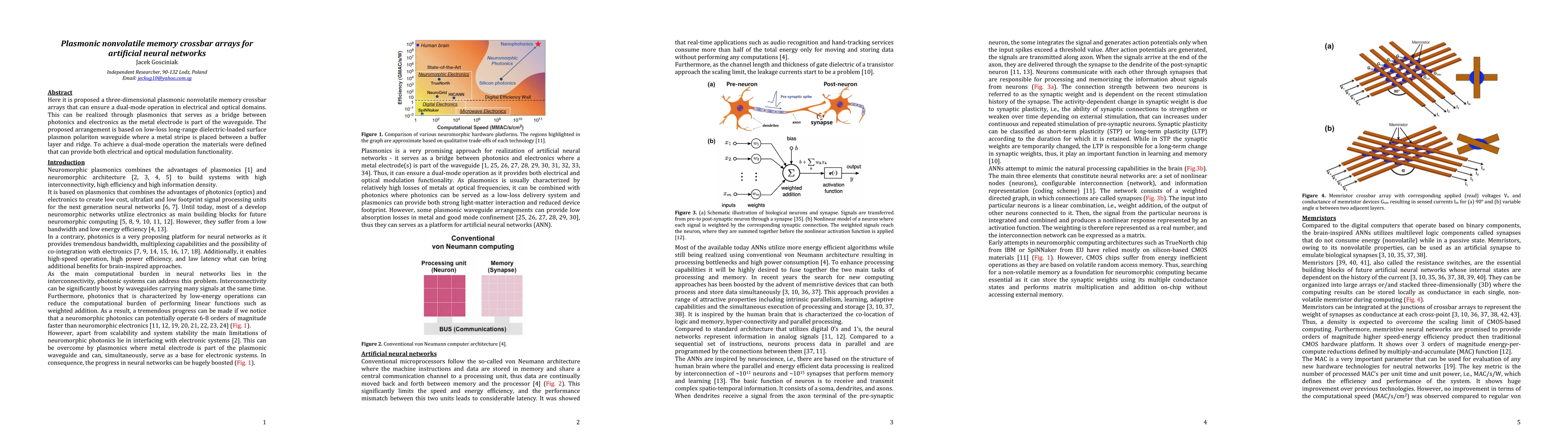
Here it is proposed a three-dimensional plasmonic nonvolatile memory crossbar arrays that can ensure a dual-mode operation in electrical and optical domains. This can be realized through plasmonics ...
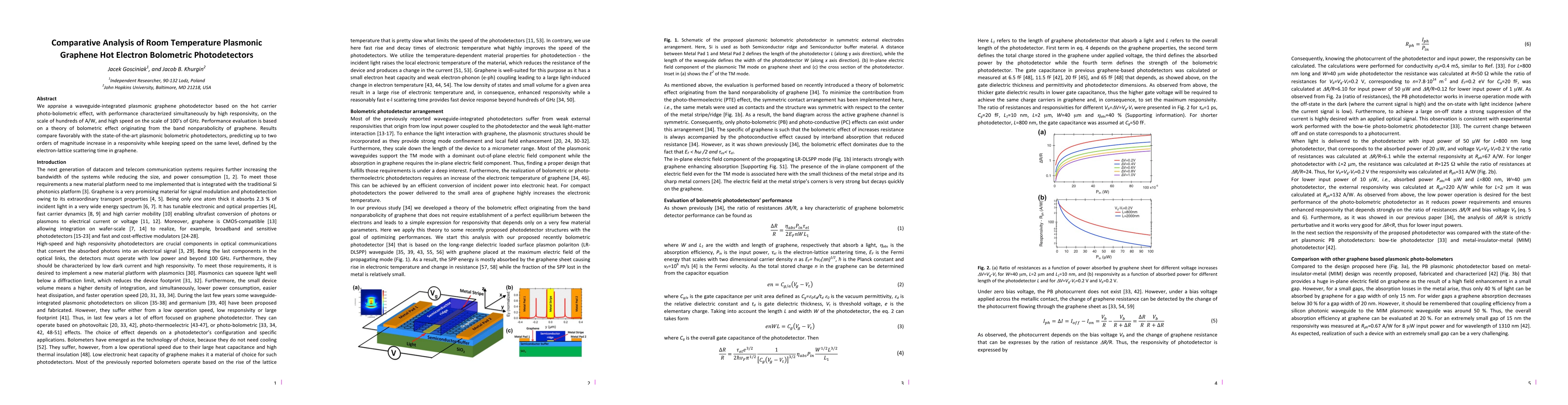
We appraise a waveguide-integrated plasmonic graphene photodetector based on the hot carrier photo-bolometric effect, with performance characterized simultaneously by high responsivity, on the scale...
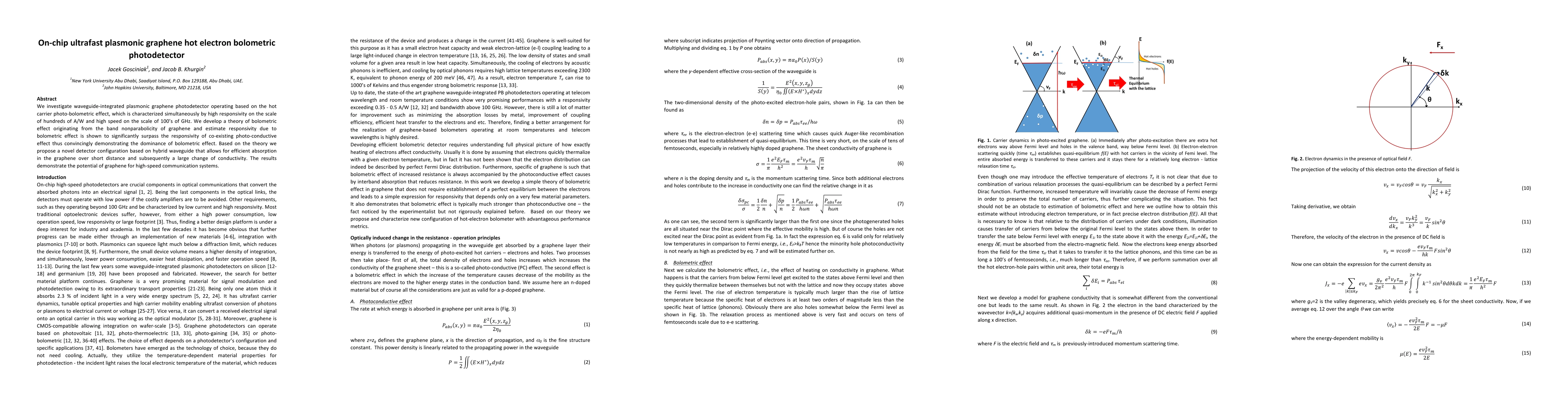
We investigate waveguide-integrated plasmonic graphene photodetector operating based on the hot carrier photo-bolometric effect, which is characterized simultaneously by high responsivity on the sca...
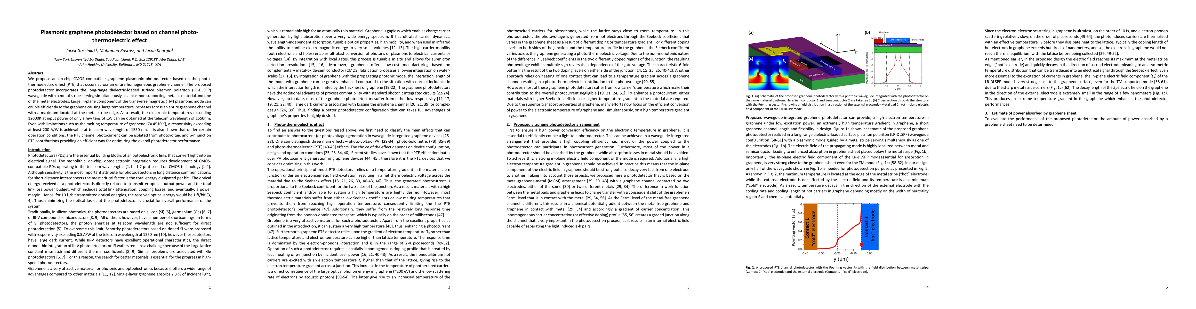
We propose an on-chip CMOS compatible graphene plasmonic photodetector based on the photo-thermoelectric effect (PTE) that occurs across an entire homogeneous graphene channel. The proposed photodet...
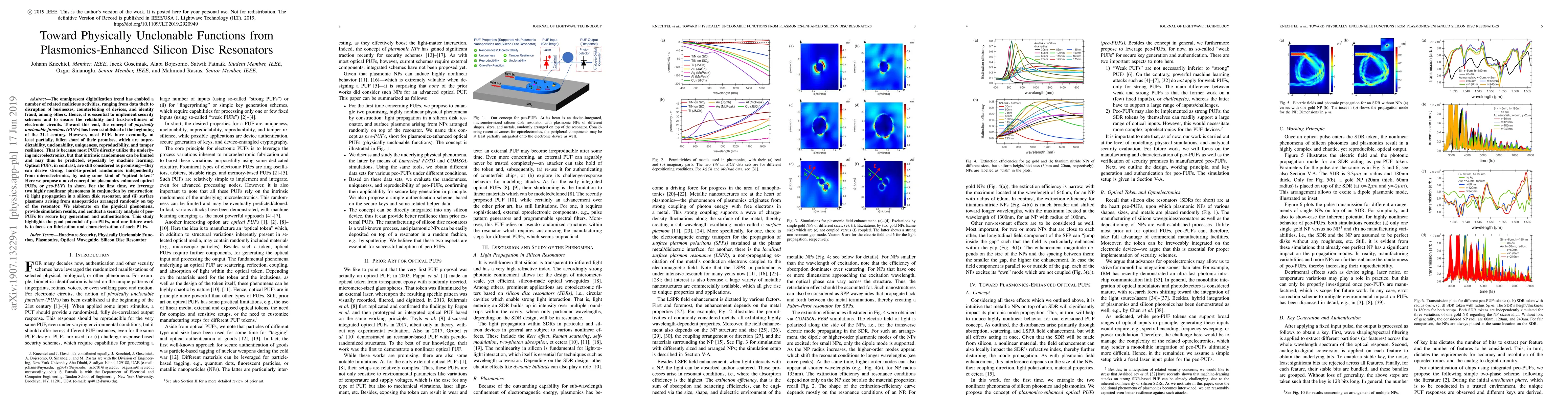
The omnipresent digitalization trend has enabled a number of related malicious activities, ranging from data theft to disruption of businesses, counterfeiting of devices, and identity fraud, among o...
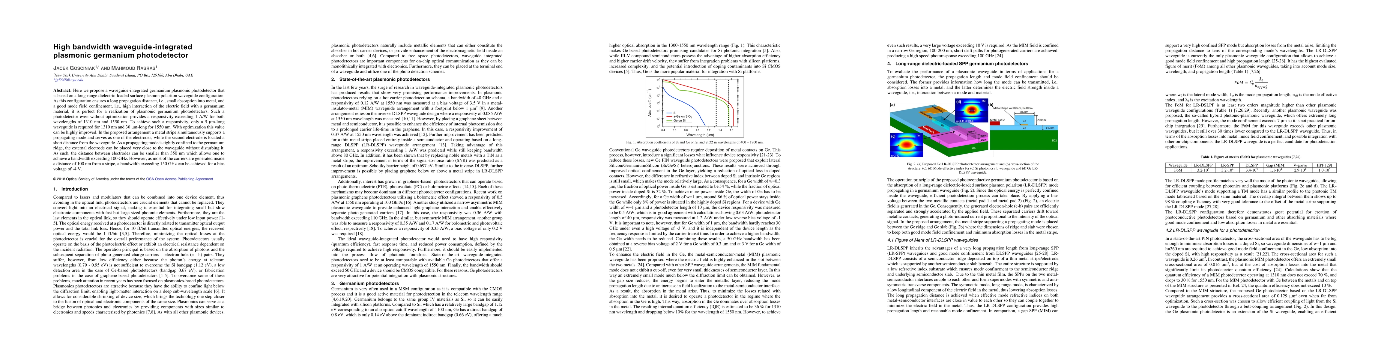
Here we propose a waveguide-integrated germanium plasmonic photodetector that is based on a long-range dielectric-loaded surface plasmon polariton waveguide configuration. As this configuration ensu...
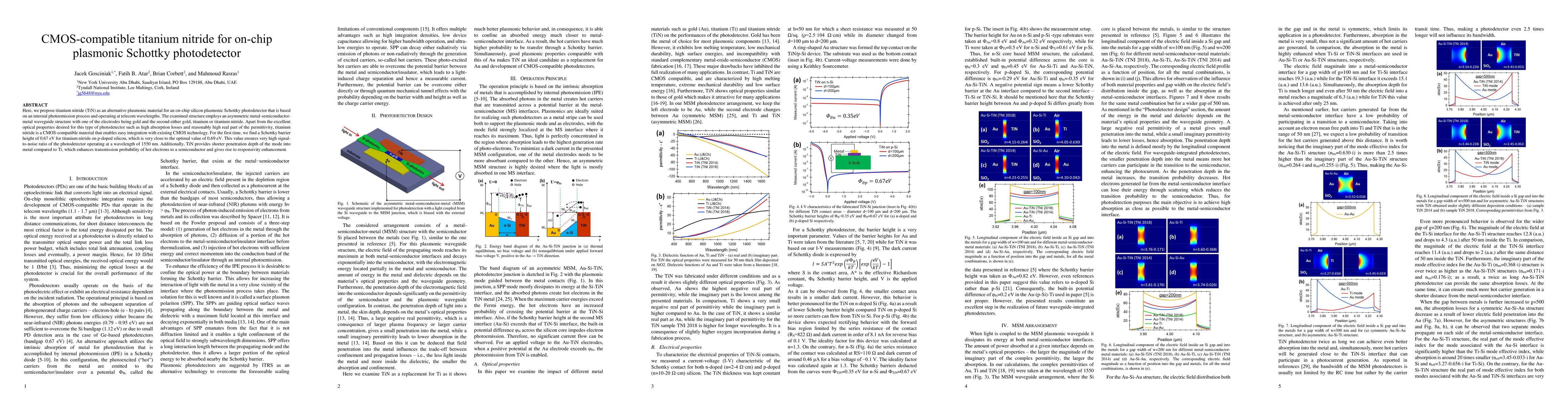
Here, we propose titanium nitride (TiN) as an alternative plasmonic material for an on-chip silicon plasmonic Schottky photodetector that is based on an internal photoemission process and operating ...
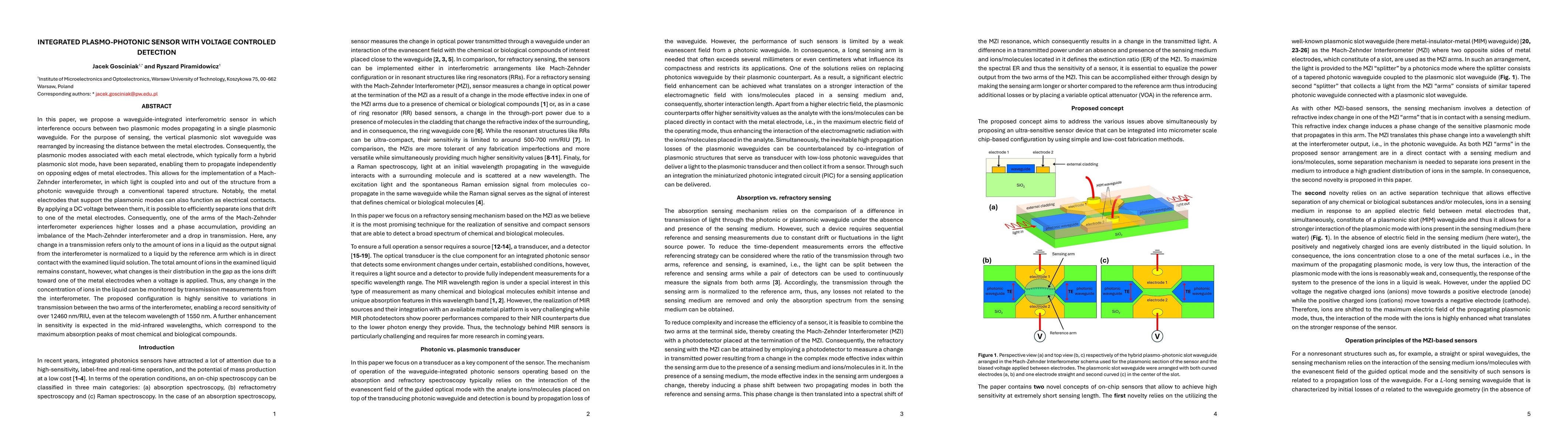
In this paper, we propose and analyze a waveguide-integrated interferometric sensor in which interference occurs between two plasmonic modes propagating in a single plasmonic waveguide. For the purpos...
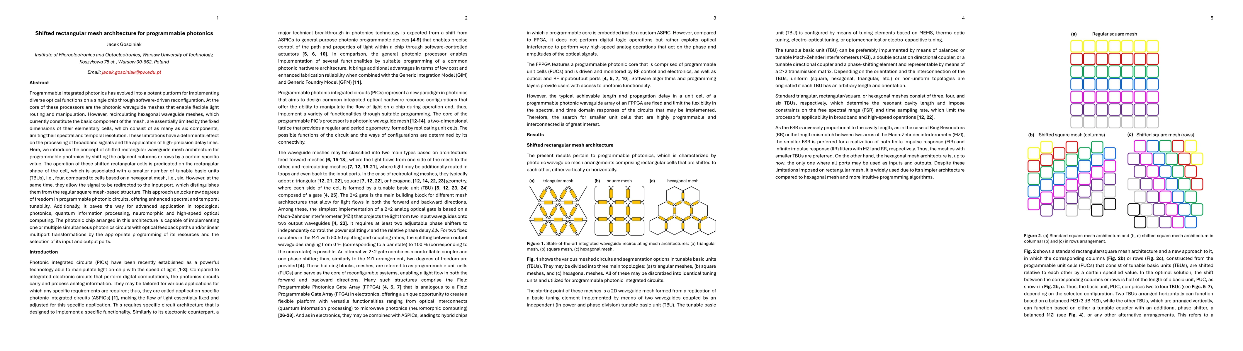
Programmable integrated photonics has evolved into a potent platform for implementing diverse optical functions on a single chip through software-driven reconfiguration. At the core of these processor...
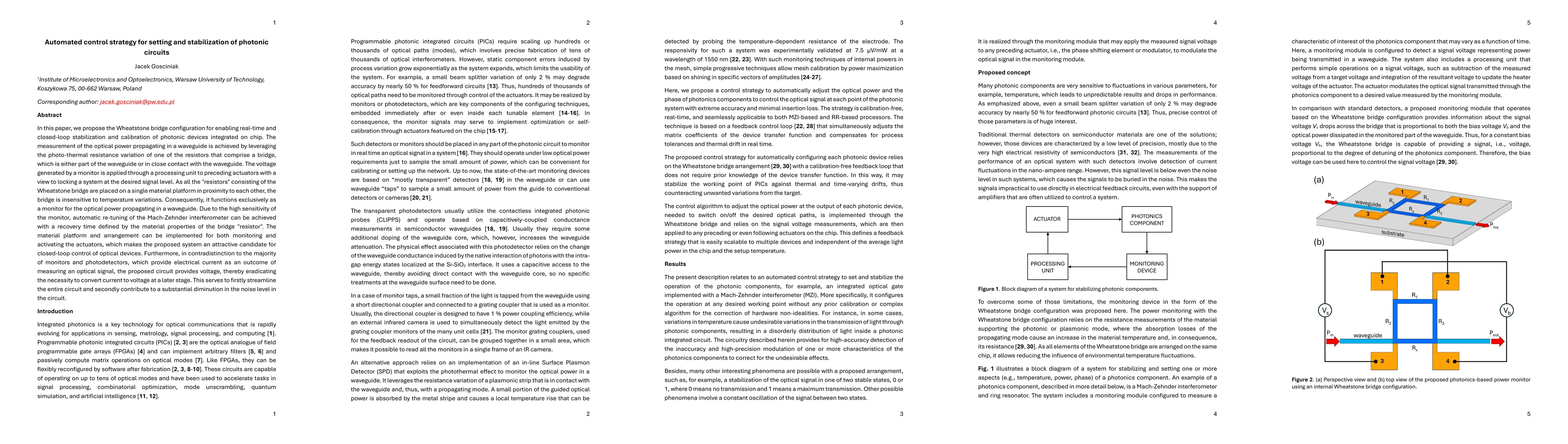
In this paper, we propose the Wheatstone bridge configuration for enabling real-time and closed-loop stabilization and calibration of photonic devices integrated on chip. The measurement of the optica...
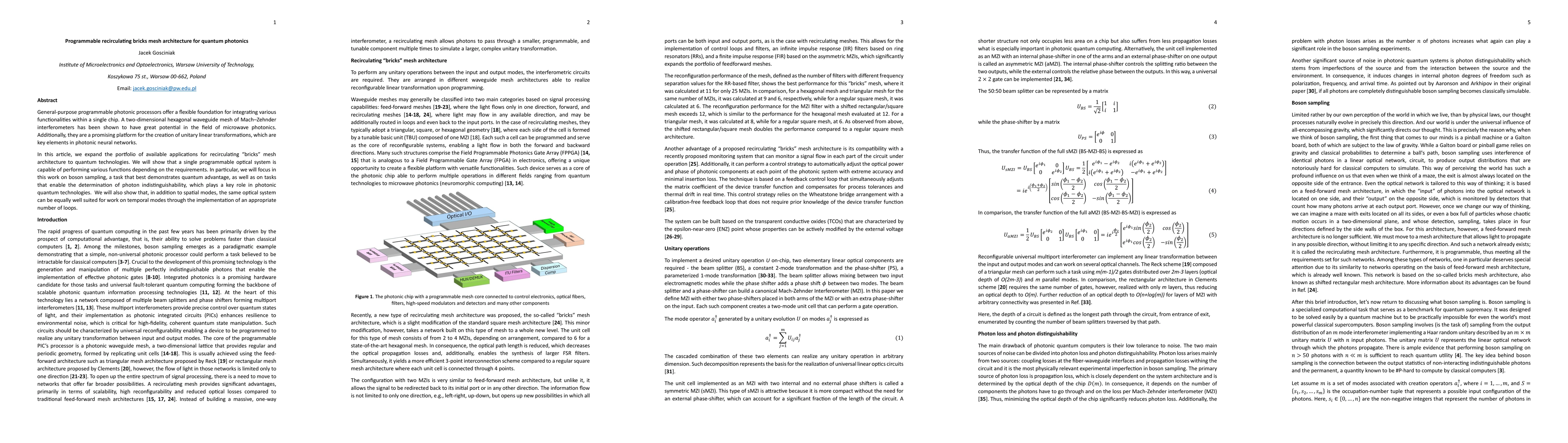
General-purpose programmable photonic processors offer a flexible foundation for integrating various functionalities within a single chip. A two-dimensional hexagonal waveguide mesh of Mach Zehnder in...
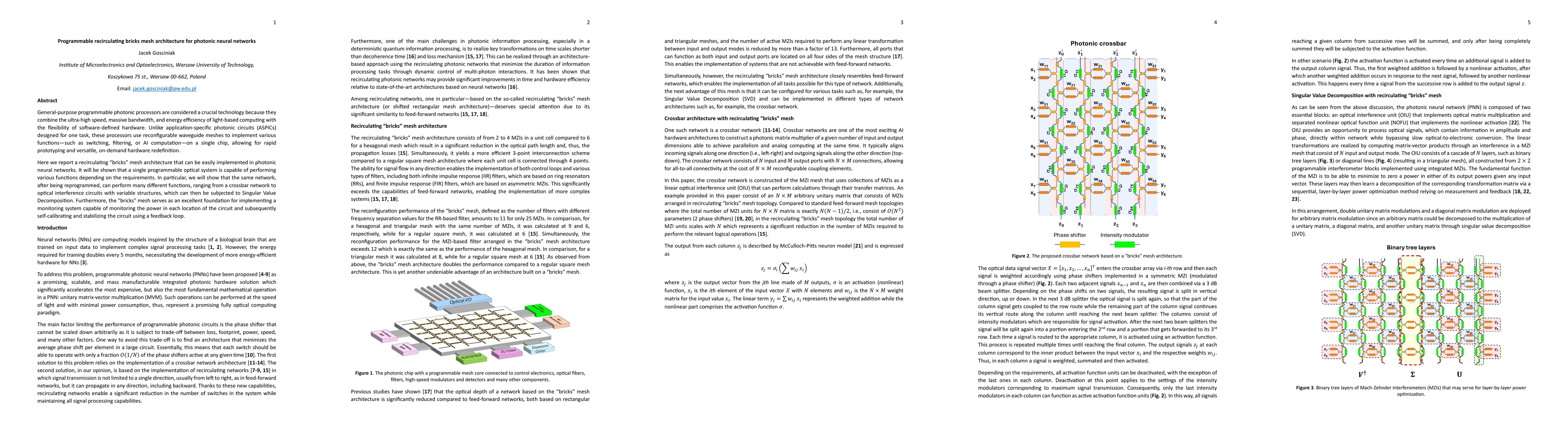
General-purpose programmable photonic processors are considered a crucial technology because they combine the ultra high-speed, massive bandwidth, and energy efficiency of light-based computing with t...
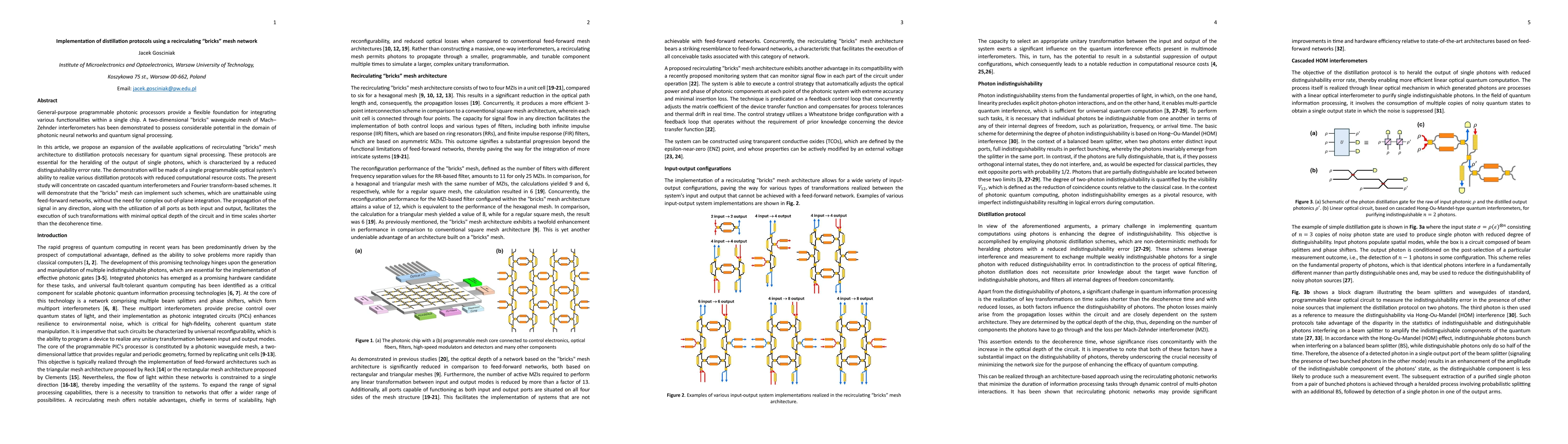
General-purpose programmable photonic processors provide a flexible foundation for integrating various functionalities within a single chip. A two-dimensional bricks waveguide mesh of Mach Zehnder int...