Academic Profile
Statistics
Similar Authors
Papers on arXiv
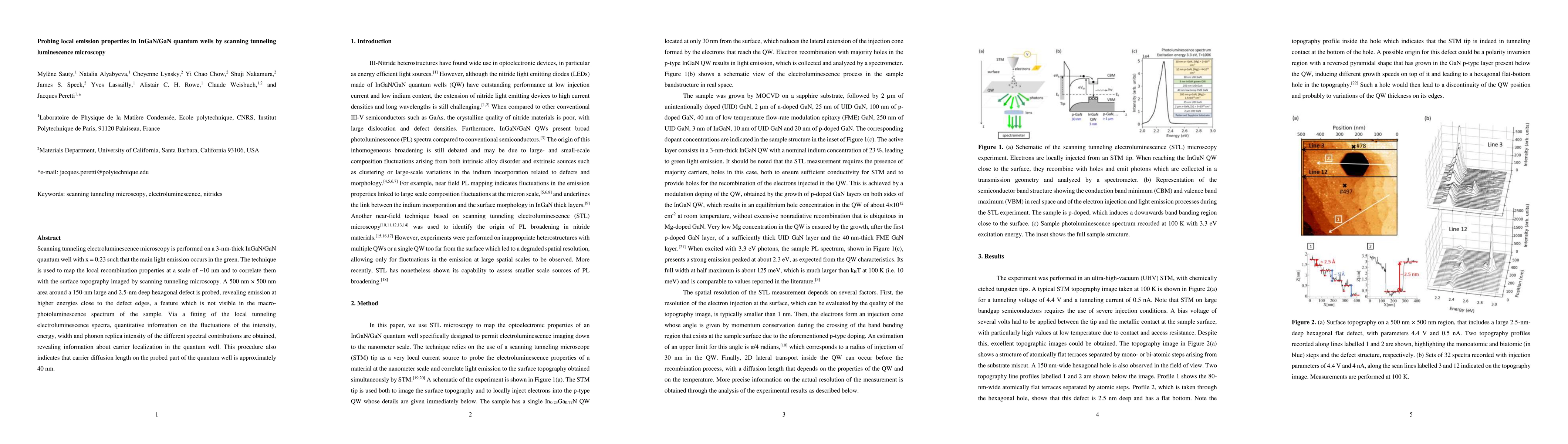
Scanning tunneling electroluminescence microscopy is performed on a 3-nm-thick InGaN/GaN quantum well with x = 0.23 such that the main light emission occurs in the green. The technique is used to ma...
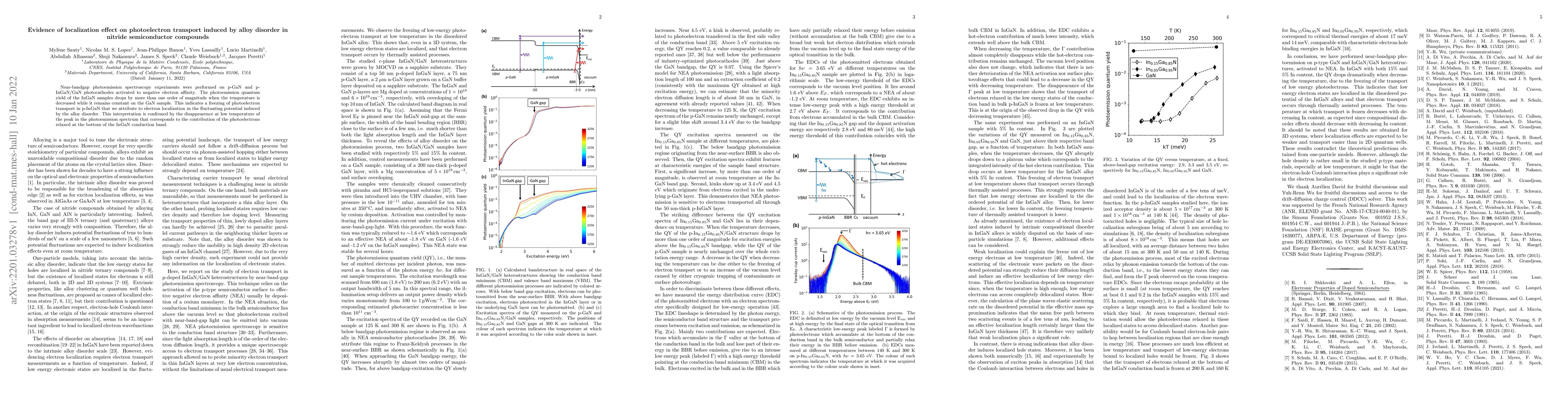
Near-bandgap photoemission spectroscopy experiments were performed on p-GaN and p-InGaN/GaN photocathodes activated to negative electron affinity. The photoemission quantum yield of the InGaN sample...
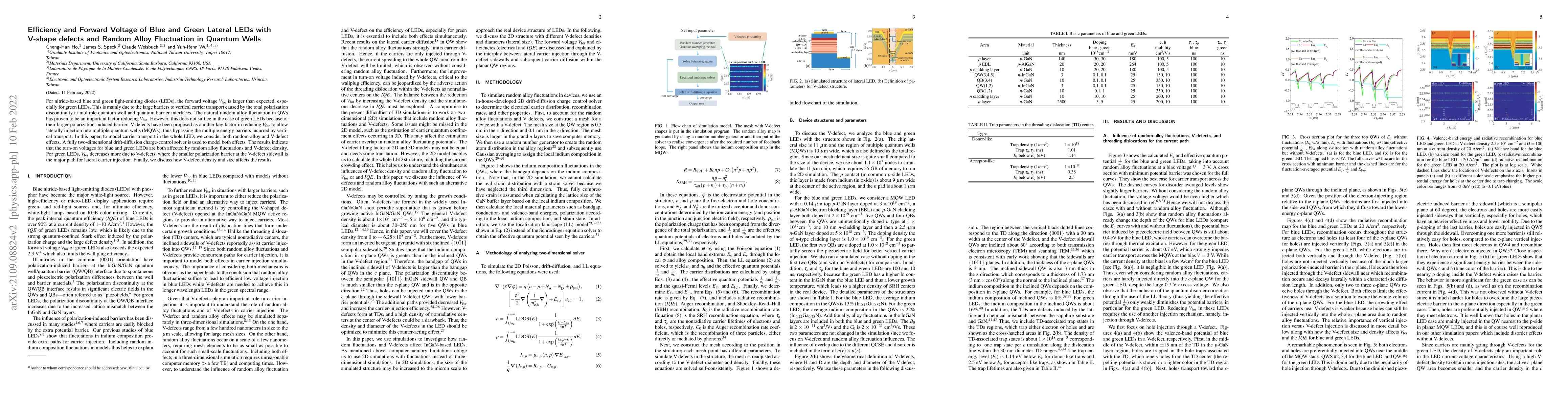
For nitride-based blue and green light-emitting diodes (LEDs), the forward voltage $V_\text{for}$ is larger than expected, especially for green LEDs. This is mainly due to the large barriers to vert...
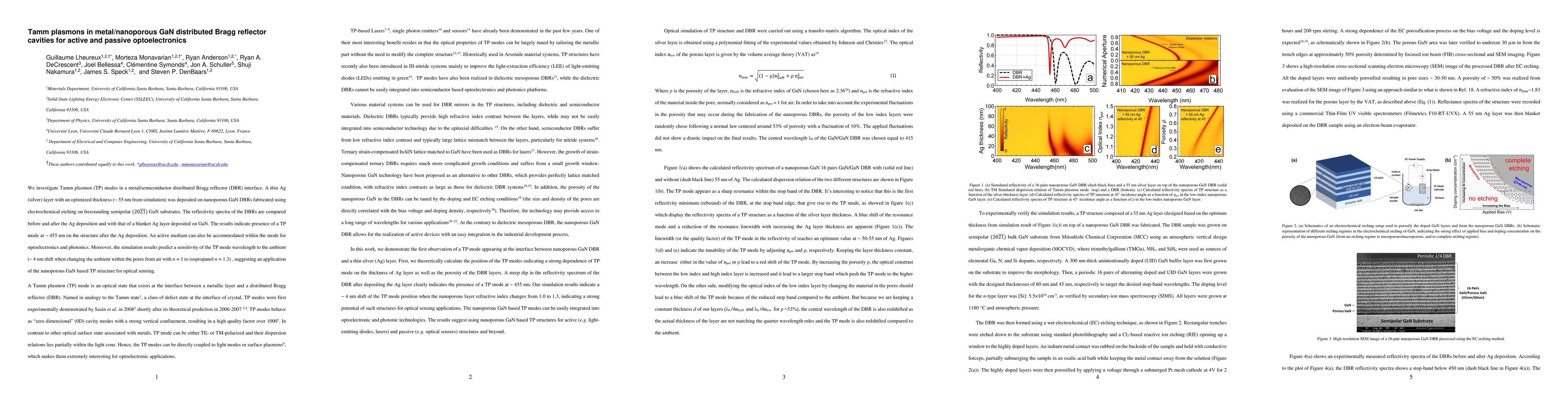
We investigate Tamm plasmon (TP) modes in a metal/semiconductor distributed Bragg reflector (DBR) interface. A thin Ag (silver) layer with an optimized thickness (~ 55 nm from simulation) was deposi...
Red InGaN-based light-emitting diodes (LEDs) exhibit lower internal quantum efficiencies (IQEs) than violet, blue, and green InGaN LEDs due to a reduction in radiative recombination rates relative to ...
The quantized electron states in the downward band bending region (BBR) at the surface of cesiated p-type GaN are investigated. We theoretically predict the existence of metastable resonant states in ...
We report the fabrication of Cr2O3/\b{eta}-Ga2O3 heterojunction diodes using reactive magnetron sputtering of Cr2O3 on highly doped \b{eta}-Ga2O3 bulk substrates along (100), (010), (001), (110), and ...
This work reports the demonstration of lateral p-NiOx/p-GaN/n-GaN-based super-heterojunction (SHJ) diodes using p-GaN with additional sputtered p-type nickel oxide (NiOx) layers to realize charge-bala...
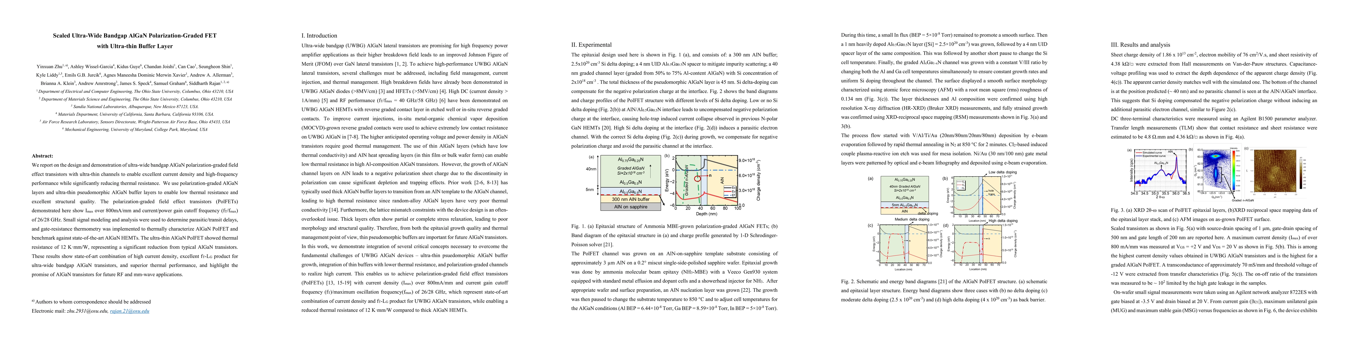
We report on the design and demonstration of ultra-wide bandgap AlGaN polarization-graded field effect transistors with ultra-thin channels to enable excellent current density and high-frequency perfo...
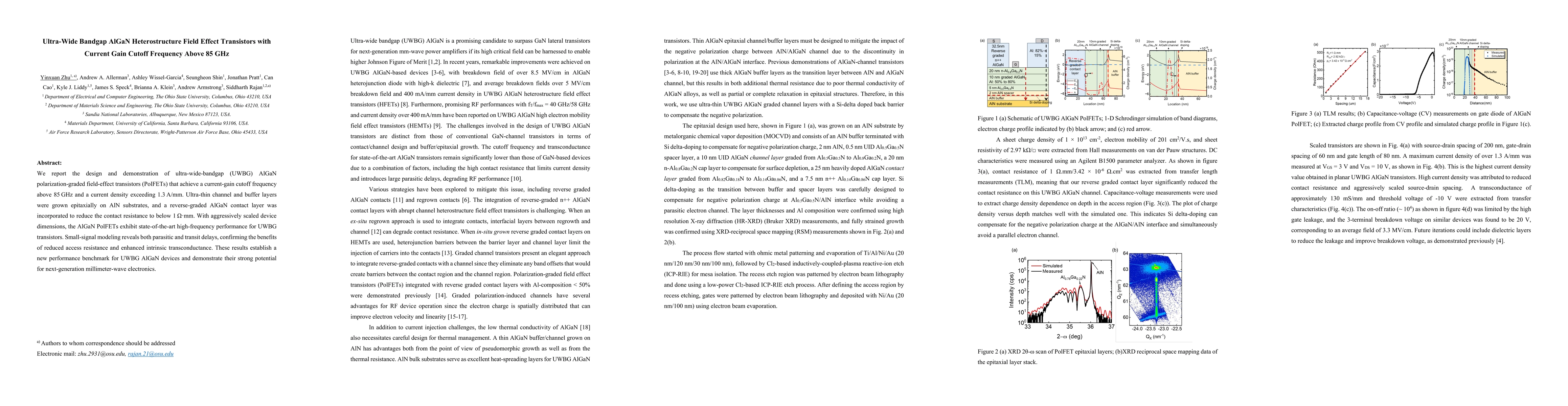
We report the design and demonstration of ultra-wide-bandgap (UWBG) AlGaN polarization-graded field-effect transistors (PolFETs) that achieve a current-gain cutoff frequency above 85 GHz and a current...
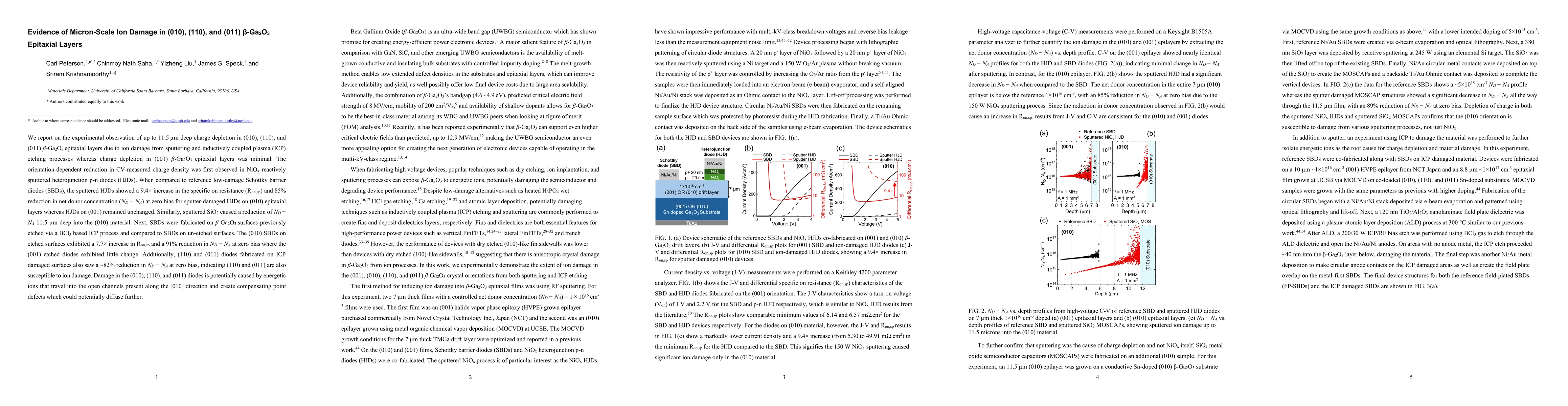
We report on the experimental observation of up to 11.5 $μm$ deep charge depletion in (010), (110), and (011) $β-Ga_2O_3$ epitaxial layers due to ion damage from sputtering and inductively coupled pla...