Academic Profile
Statistics
Similar Authors
Papers on arXiv
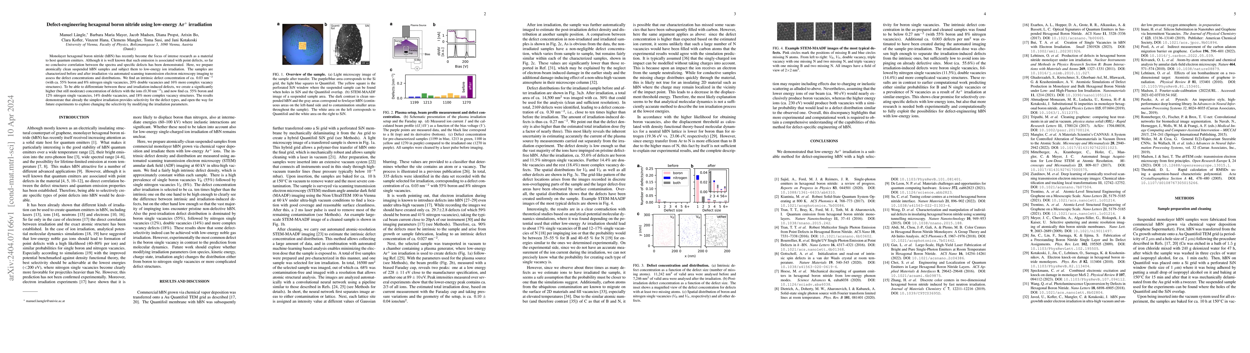
Monolayer hexagonal boron nitride (hBN) has recently become the focus of intense research as a material to host quantum emitters. Although it is well known that such emission is associated with poin...
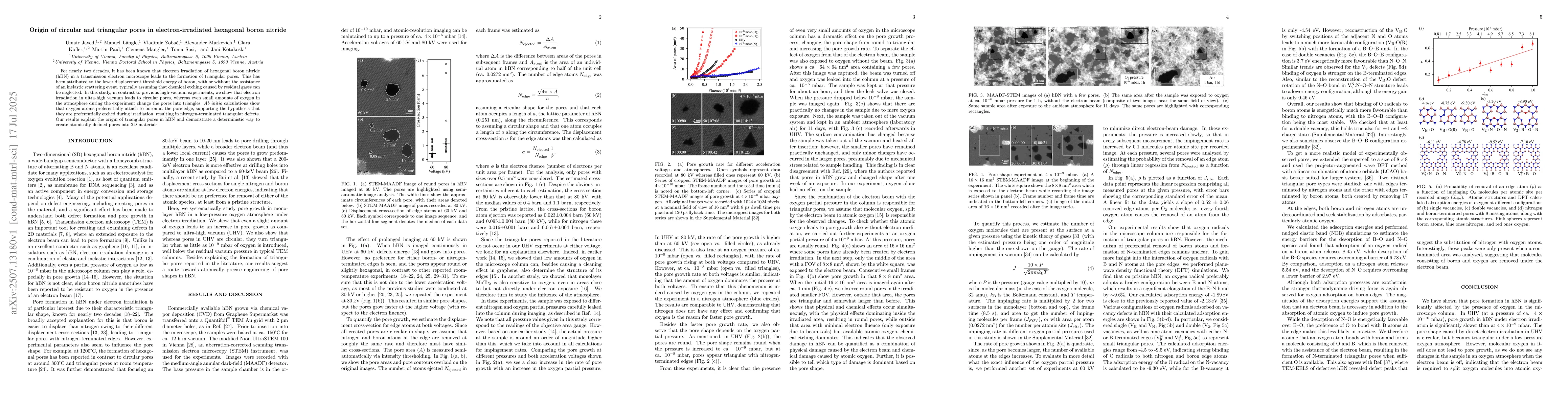
Control of water ice formation on surfaces is of key technological and economic importance, but the fundamental understanding of ice nucleation and growth mechanisms and the design of surfaces for c...
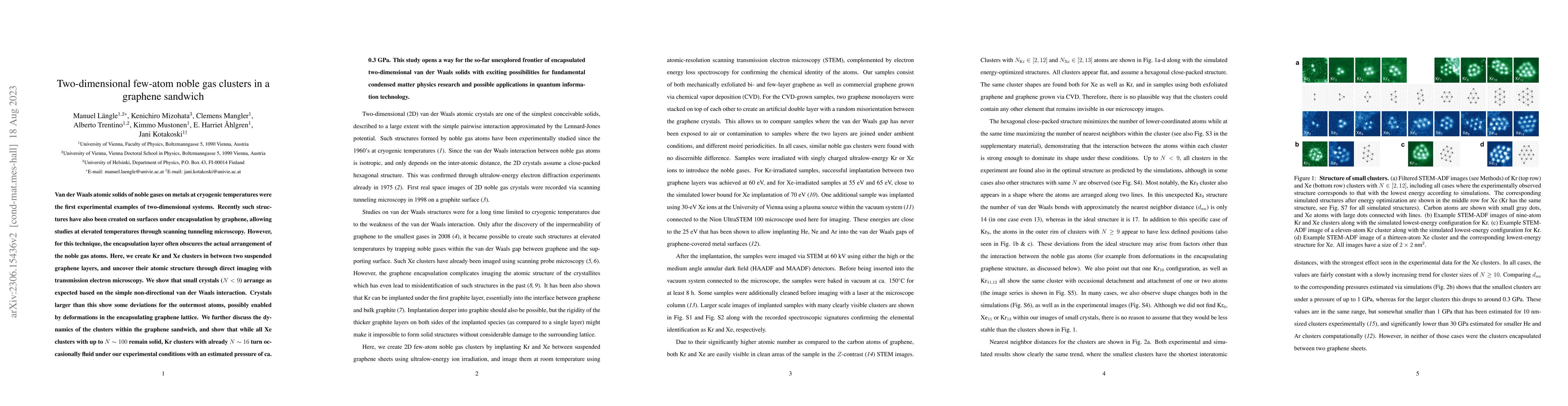
Van der Waals atomic solids of noble gases on metals at cryogenic temperatures were the first experimental examples of two-dimensional systems. Recently such structures have also been created on sur...
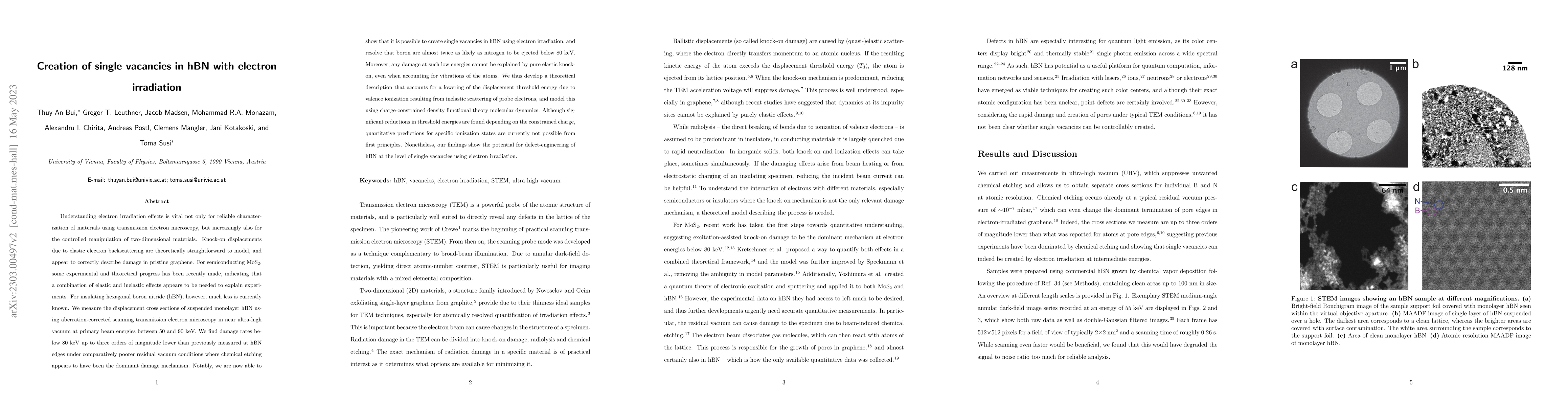
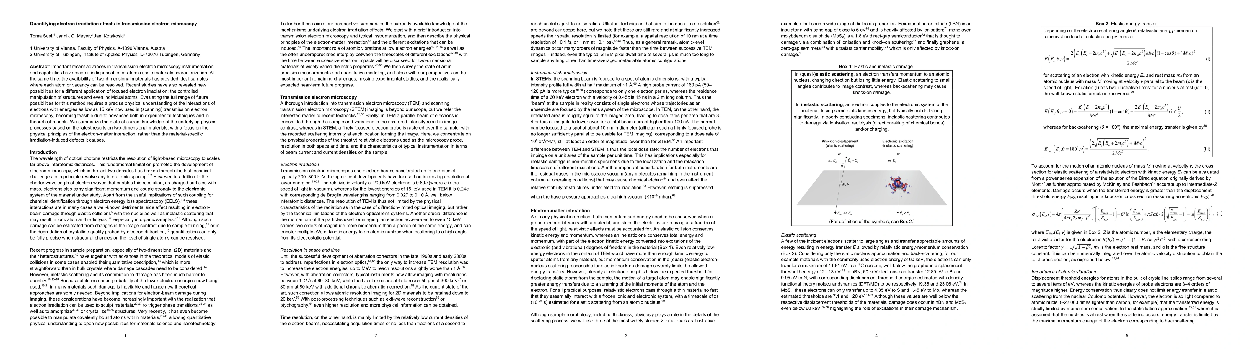
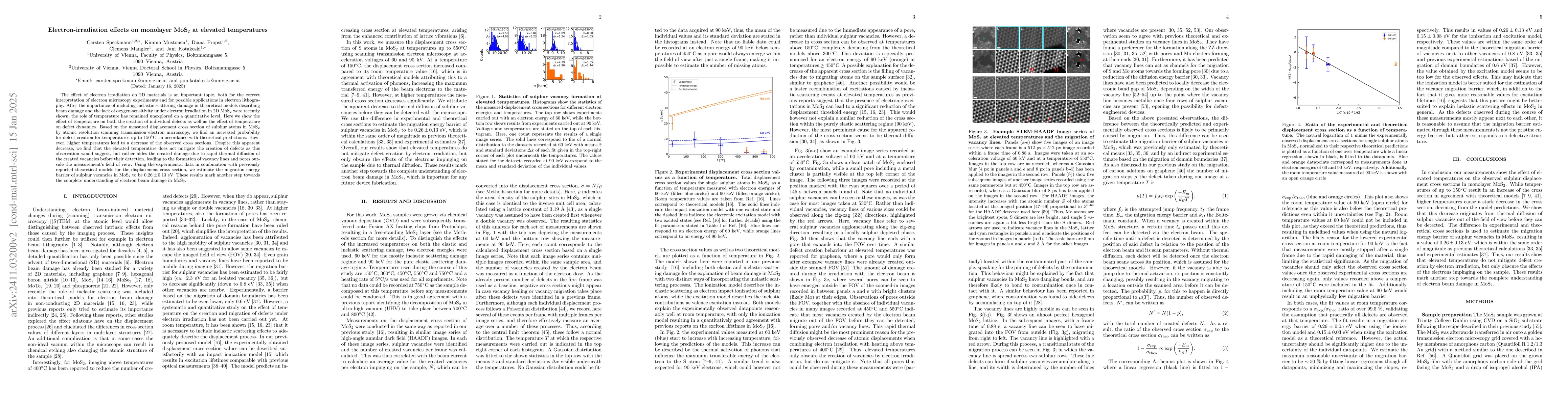
Understanding electron irradiation effects is vital not only for reliable transmission electron microscopy characterization, but increasingly also for the controlled manipulation of two-dimensional ...
Electron irradiation-induced damage is often the limiting factor in imaging materials prone to ionization or electronic excitations due to inelastic electron scattering. Quantifying the related proc...
Some of the materials are more affected by oxidation than others. To elucidate the oxidation-induced degradation mechanisms in transition metal chalcogenides, the chemical effects in single layer Mo...
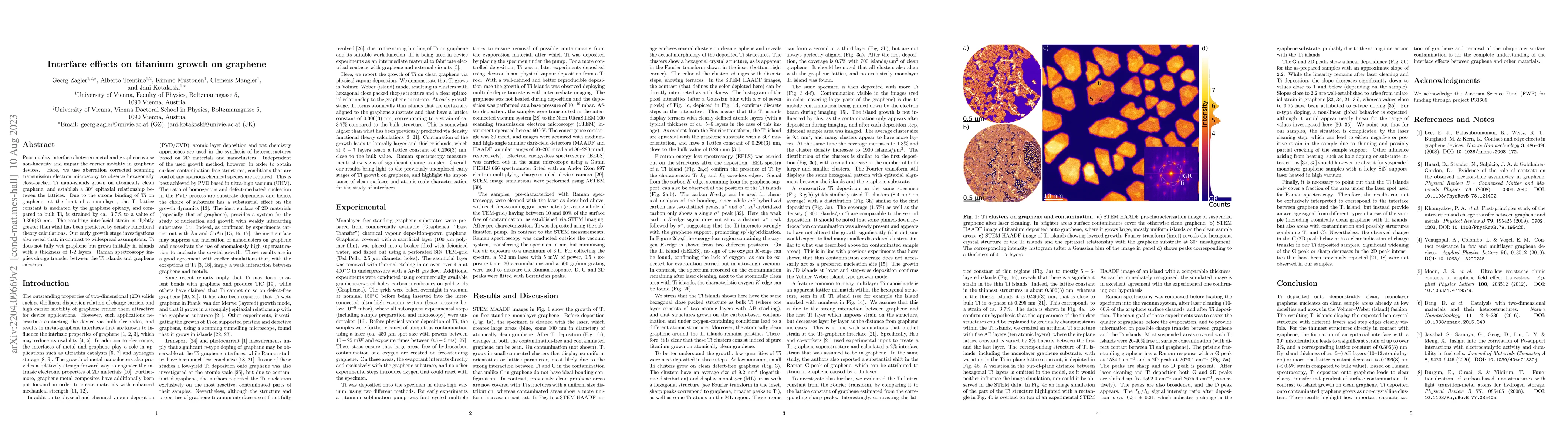
Poor quality interfaces between metal and graphene cause non-linearity and impair the carrier mobility in graphene devices. Here, we use aberration corrected scanning transmission electron microscop...
Although surface diffusion is critical for many physical and chemical processes, including the epitaxial growth of crystals and heterogeneous catalysis, it is particularly challenging to directly st...
Elastic knock-on is the main electron irradiation damage mechanism in metals including graphene. Atomic vibrations influence its cross-section, but only the out-of-plane direction has been considere...
Heterostructures composed of two-dimensional (2D) materials are already opening many new possibilities in such fields of technology as electronics and magnonics, but far more could be achieved if th...
A boost in the development of flexible and wearable electronics facilitates the design of new materials to be applied as transparent conducting films (TCFs). Although single-walled carbon nanotube (...
Transmission electron microscopy (TEM) and scanning TEM (STEM) are indispensable tools for materials characterization. However, during a typical (S)TEM experiment, the sample is subject to a number ...
Single atoms and few-atom nanoclusters are of high interest in catalysis and plasmonics, but pathways for their fabrication and stable placement remain scarce. We report here the self-assembly of ro...
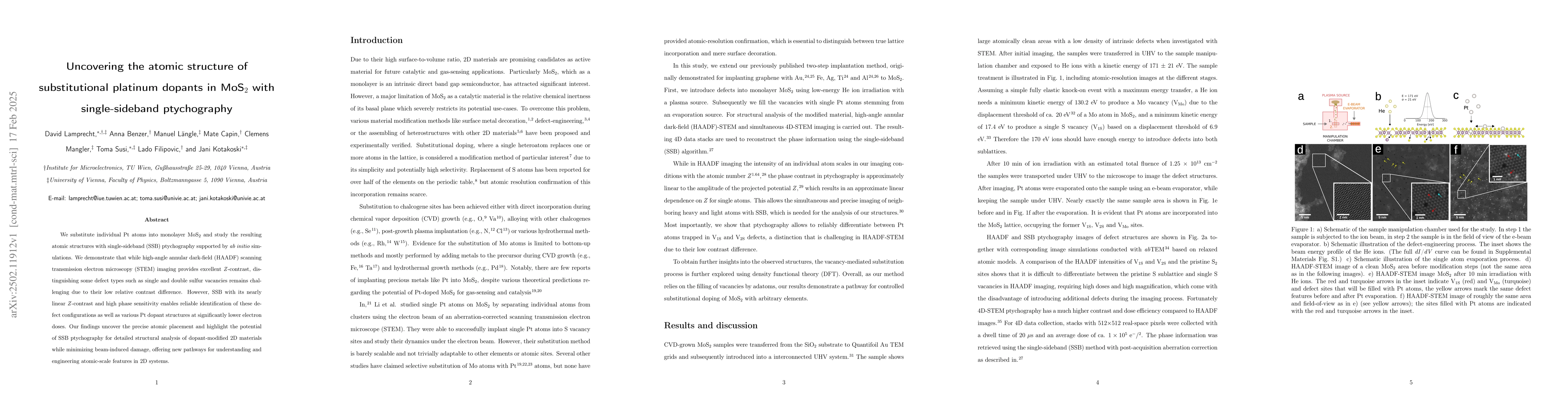
Important recent advances in transmission electron microscopy instrumentation and capabilities have made it indispensable for atomic-scale materials characterization. At the same time, the availabil...
Growth of two-dimensional metals has eluded materials scientists since the discovery of the atomically thin graphene and other covalently bound 2D materials. Here, we report a two-atom-thick hexagon...
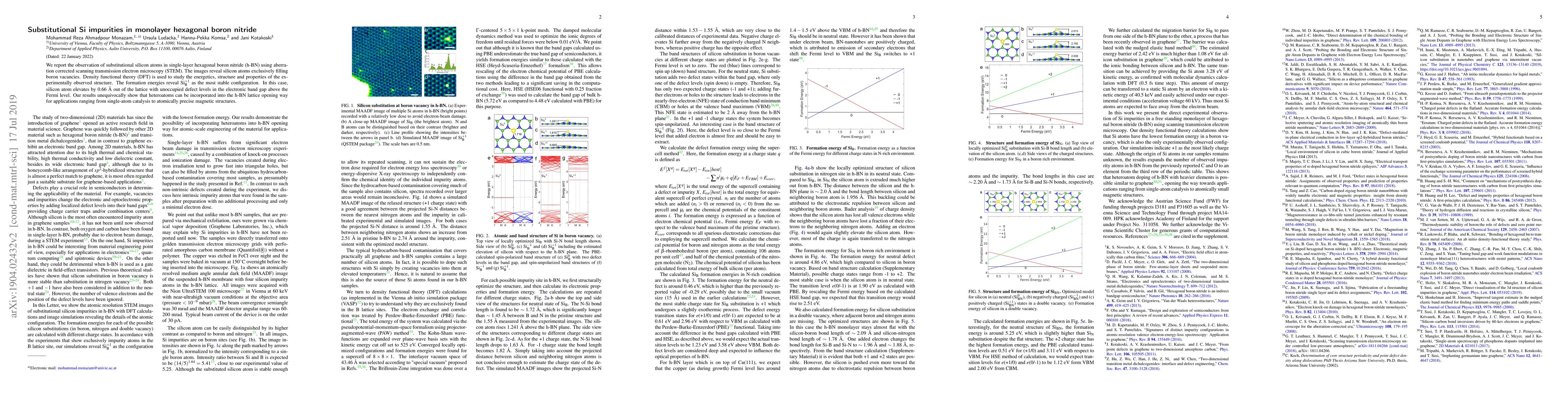
We report the first observation of substitutional silicon atoms in single-layer hexagonal boron nitride (h-BN) using aberration corrected scanning transmission electron microscopy (STEM). The medium...
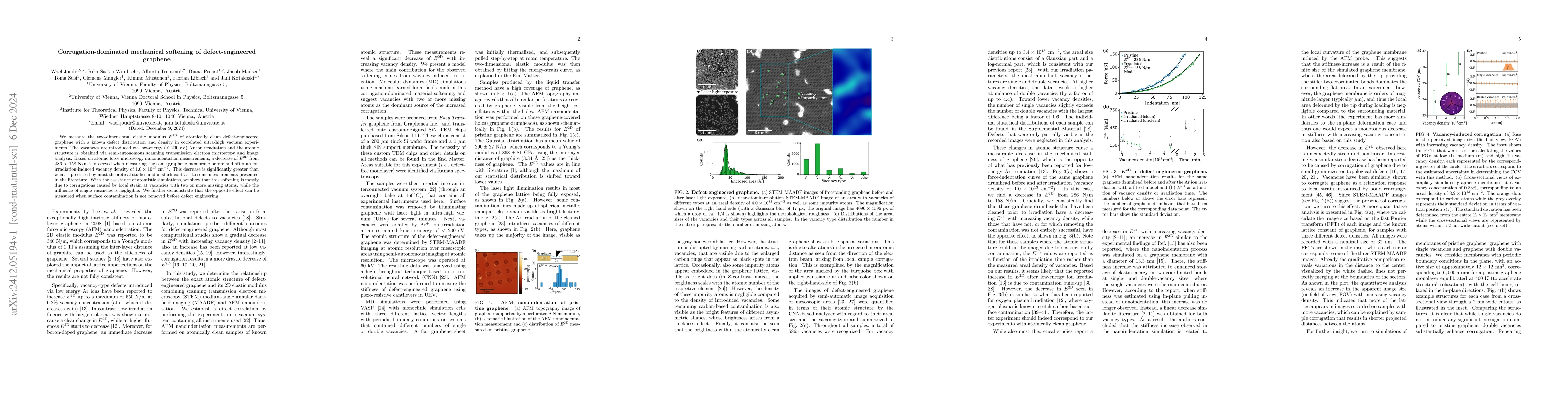
We measure the two-dimensional elastic modulus $E^\text{2D}$ of atomically clean defect-engineered graphene with a known defect distribution and density in correlated ultra-high vacuum experiments. Th...
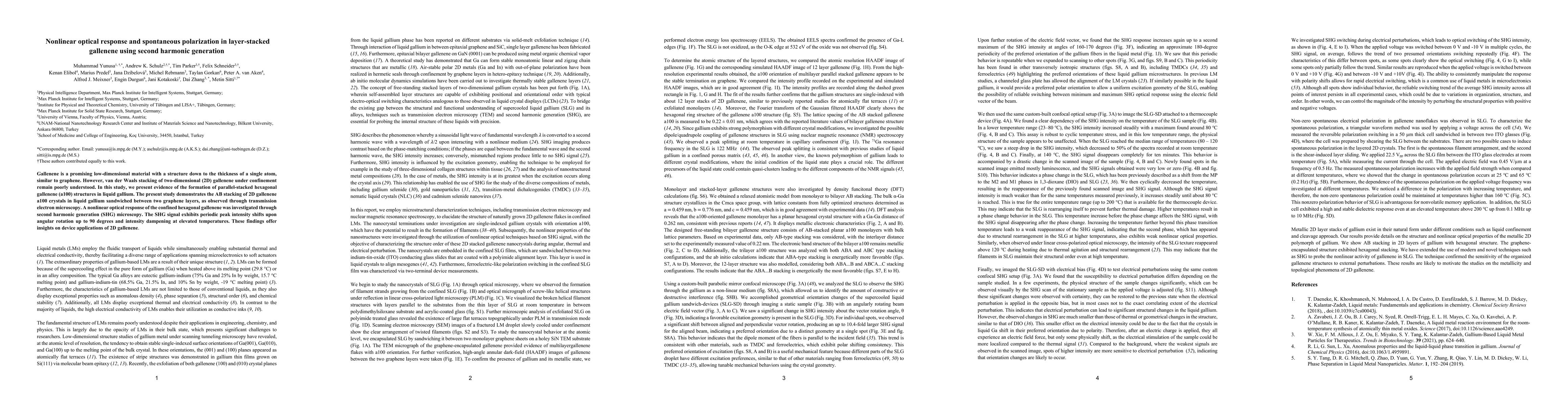
Gallenene is a promising low-dimensional material with a structure down to the thickness of a single atom, similar to graphene. However, van der Waals stacking of two-dimensional (2D) gallenene under ...
The effect of electron irradiation on 2D materials is an important topic, both for the correct interpretation of electron microscopy experiments and for possible applications in electron lithography. ...
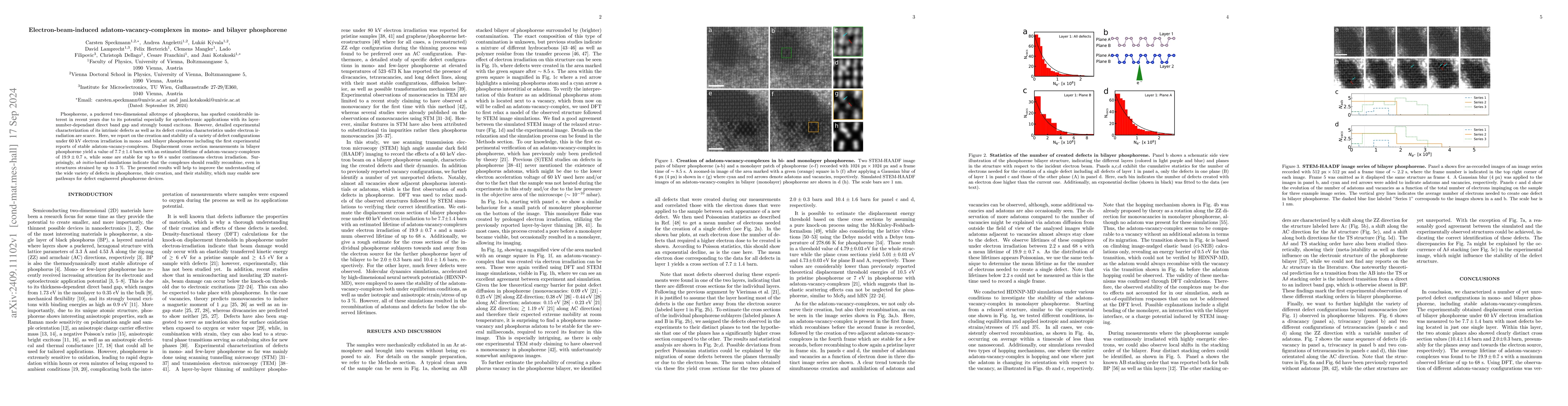
Phosphorene, a puckered two-dimensional allotrope of phosphorus, has sparked considerable interest in recent years due to its potential especially for optoelectronic applications with its layer-number...
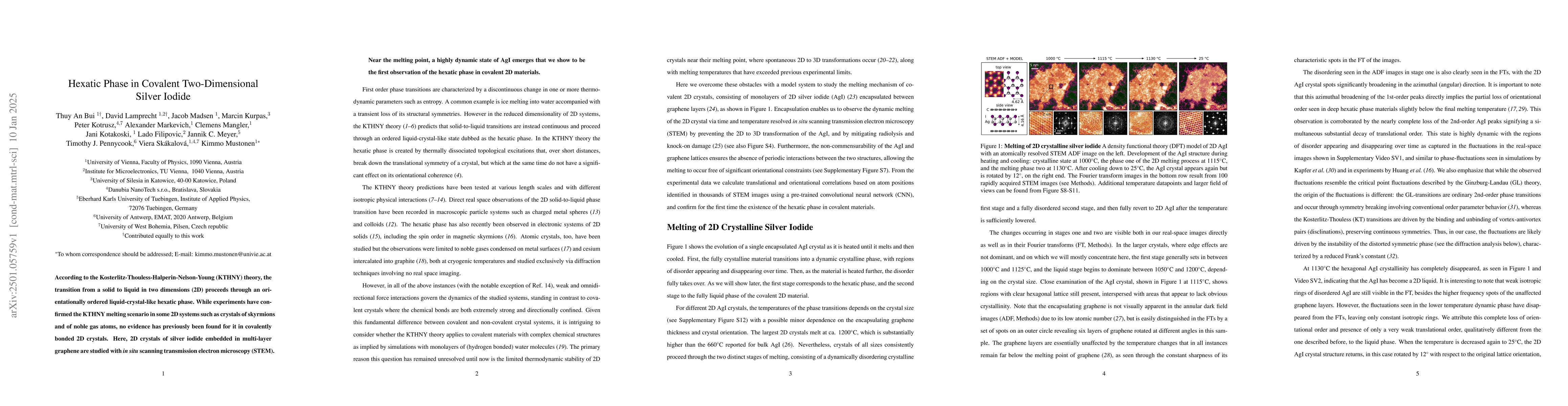
According to the Kosterlitz-Thouless-Halperin-Nelson-Young (KTHNY) theory, the transition from a solid to liquid in two dimensions (2D) proceeds through an orientationally ordered liquid-crystal-like ...
We substitute individual Pt atoms into monolayer MoS$_2$ and study the resulting atomic structures with single-sideband (SSB) ptychography supported by ab initio simulations. We demonstrate that while...
For nearly two decades, it has been known that electron irradiation of hexagonal boron nitride (hBN) in a transmission electron microscope leads to the formation of triangular pores. This has been att...
Surface contamination not only influences but in some cases even dominates the measured properties of two-dimensional materials. Although different cleaning methods are often used for contamination re...
There is a growing interest in identifying the origin of single-photon emission in hexagonal boron nitride (hBN), with proposed candidates including boron and nitrogen vacancies as well as carbon subs...
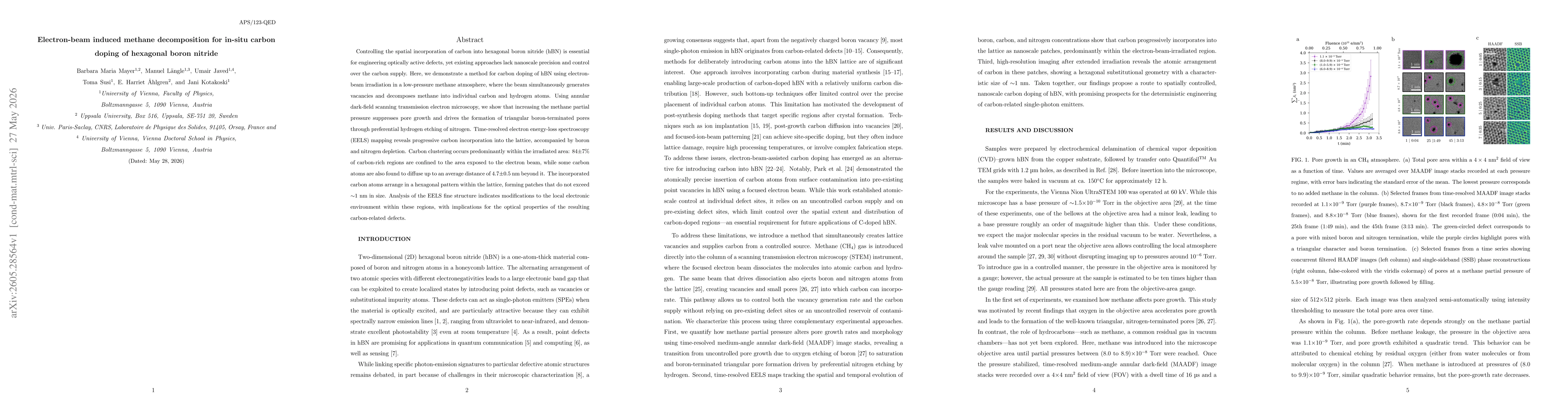
Controlling the spatial incorporation of carbon into hexagonal boron nitride (hBN) is essential for engineering optically active defects, yet existing approaches lack nanoscale precision and control o...