Academic Profile
Statistics
Similar Authors
Papers on arXiv
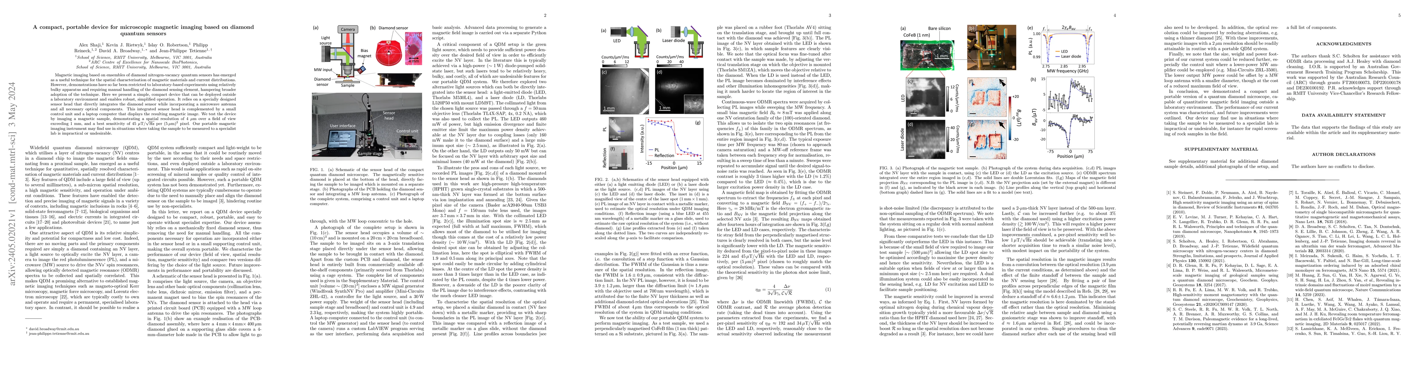
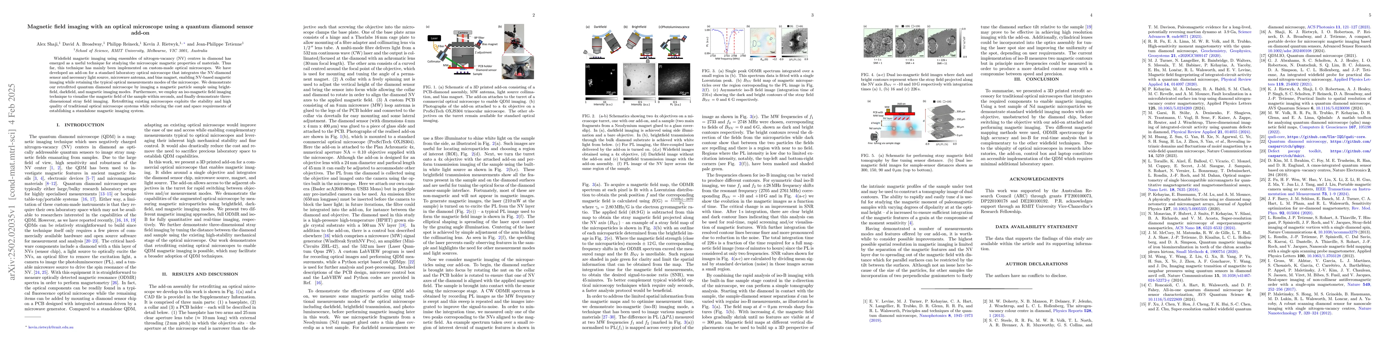
Magnetic imaging based on ensembles of diamond nitrogen-vacancy quantum sensors has emerged as a useful technique for the spatial characterisation of magnetic materials and current distributions. Ho...
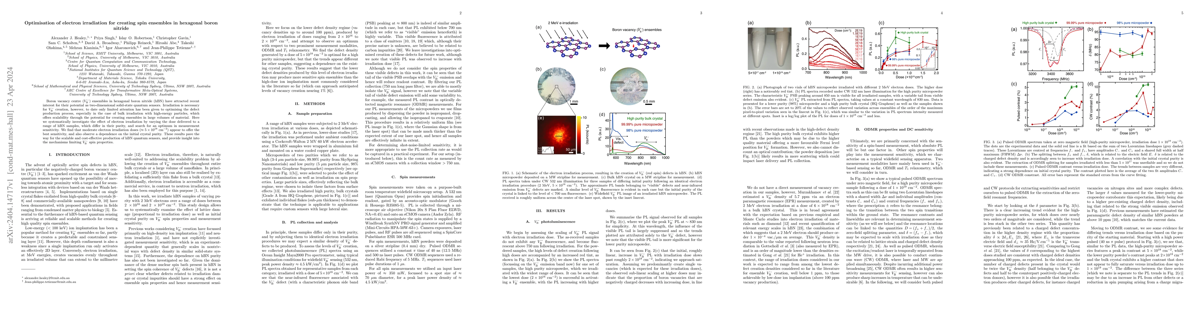
Boron vacancy centre ($V_{\rm B}^-$) ensembles in hexagonal boron nitride (hBN) have attracted recent interest for their potential as two-dimensional solid-state quantum sensors. Irradiation is nece...
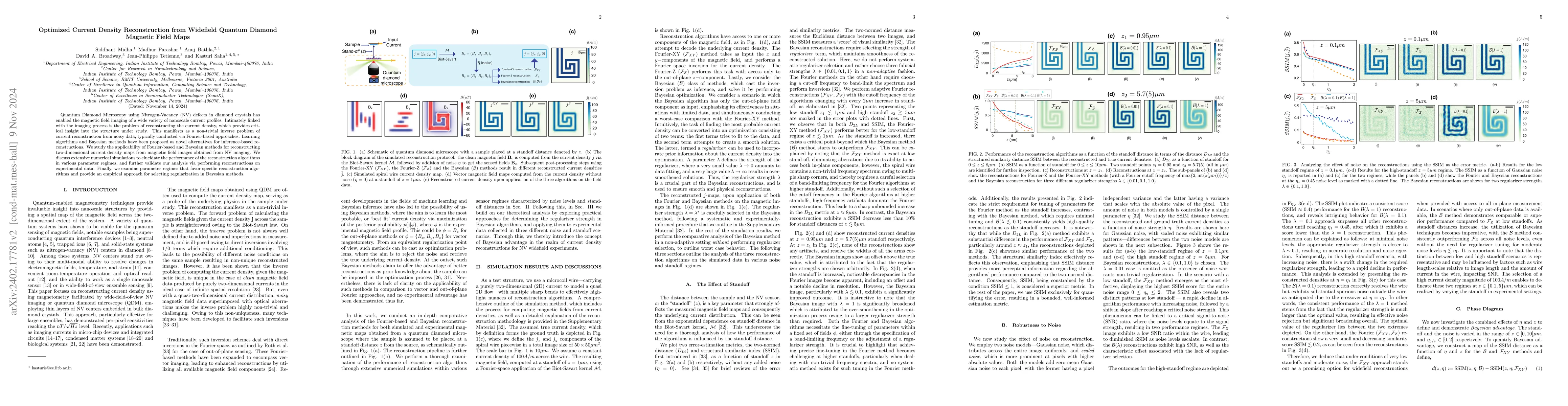
Quantum Diamond Microscopy using Nitrogen-Vacancy (NV) defects in diamond crystals has enabled the magnetic field imaging of a wide variety of nanoscale current profiles. Intimately linked with the ...
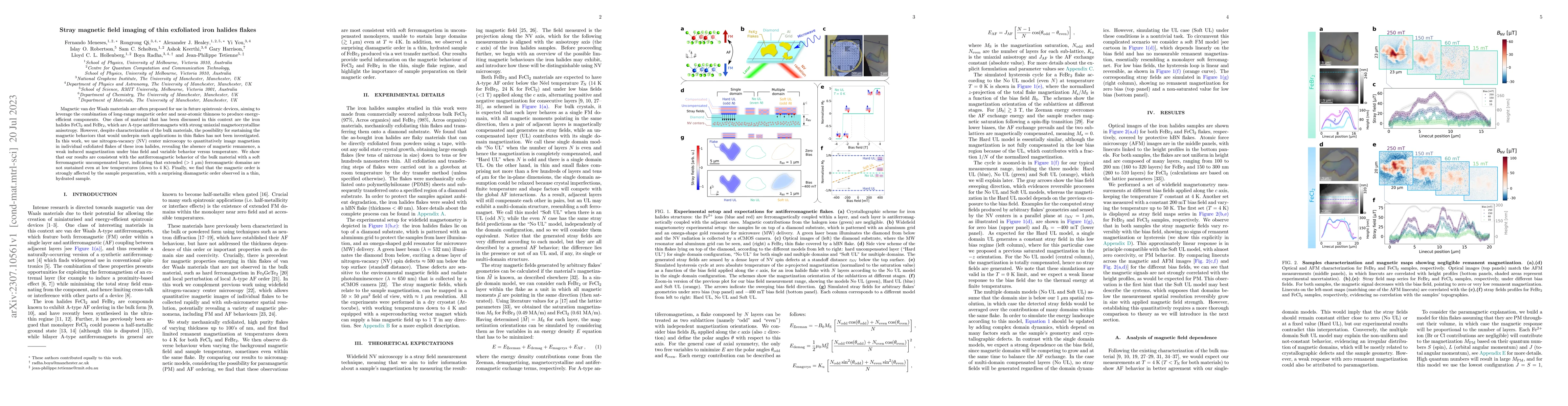
Magnetic van der Waals materials are often proposed for use in future spintronic devices, aiming to leverage the combination of long-range magnetic order and near-atomic thinness to produce energy-e...
Optically addressable spin defects hosted in two-dimensional van der Waals materials represent a new frontier for quantum technologies, promising to lead to a new class of ultrathin quantum sensors ...
Detecting magnetic noise from small quantities of paramagnetic spins is a powerful capability for chemical, biochemical, and medical analysis. Quantum sensors based on optically addressable spin def...
Van der Waals (vdW) magnets are appealing candidates for realising spintronic devices that exploit current control of magnetization (e.g. switching or domain wall motion), but so far experimental de...
The recent isolation of two-dimensional van der Waals magnetic materials has uncovered rich physics that often differs from the magnetic behaviour of their bulk counterparts. However, the microscopi...
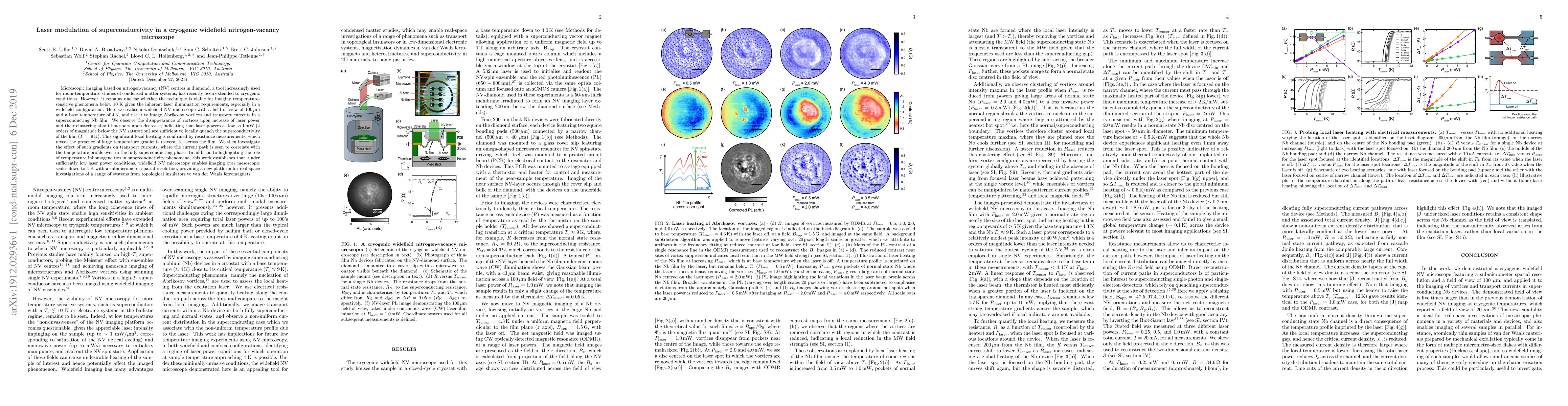
Microscopic imaging based on nitrogen-vacancy (NV) centres in diamond, a tool increasingly used for room-temperature studies of condensed matter systems, has recently been extended to cryogenic cond...
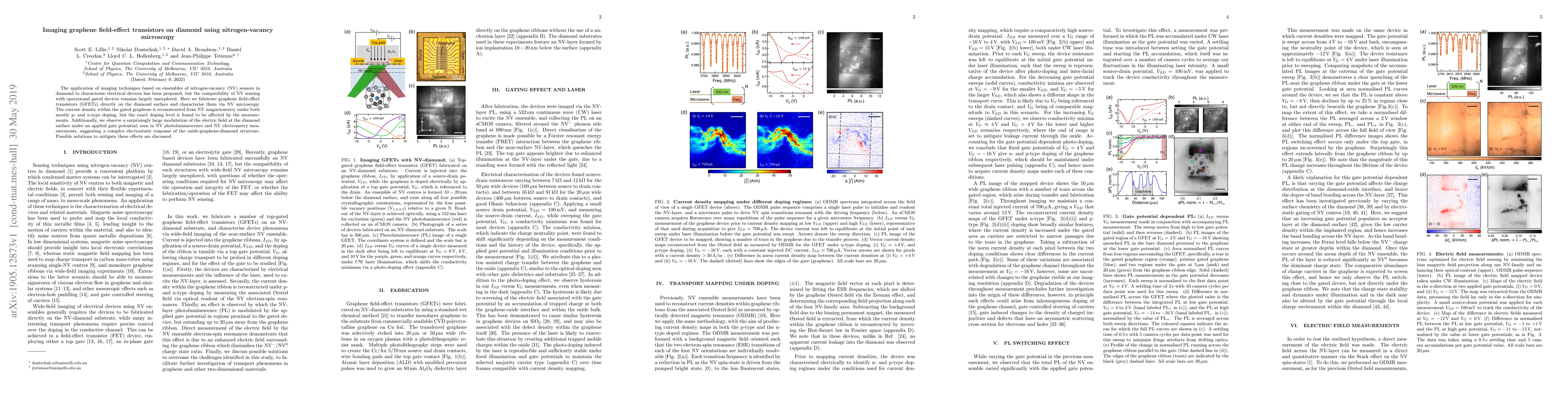
The application of imaging techniques based on ensembles of nitrogen-vacancy (NV) sensors in diamond to characterise electrical devices has been proposed, but the compatibility of NV sensing with op...
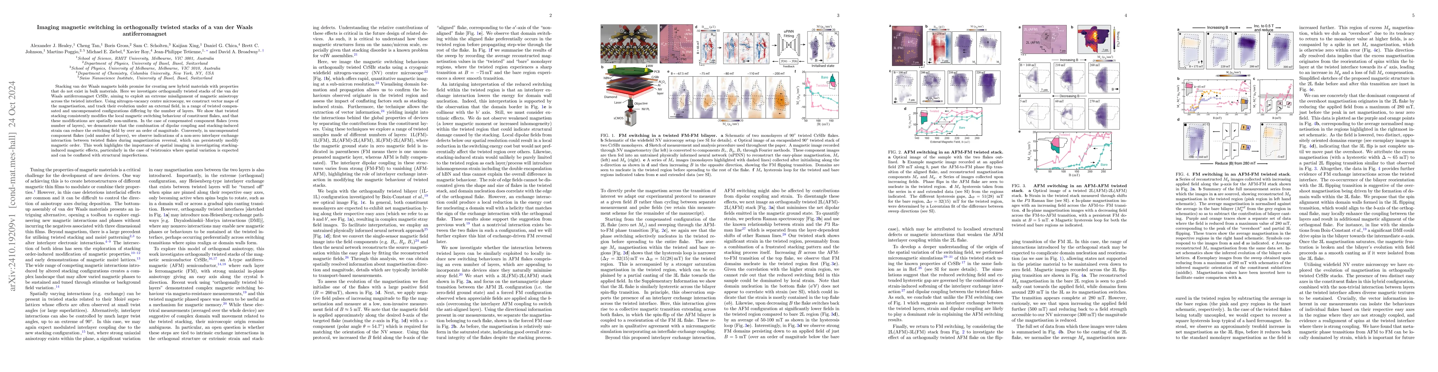
Stacking van der Waals magnets holds promise for creating new hybrid materials with properties that do not exist in bulk materials. Here we investigate orthogonally twisted stacks of the van der Waals...
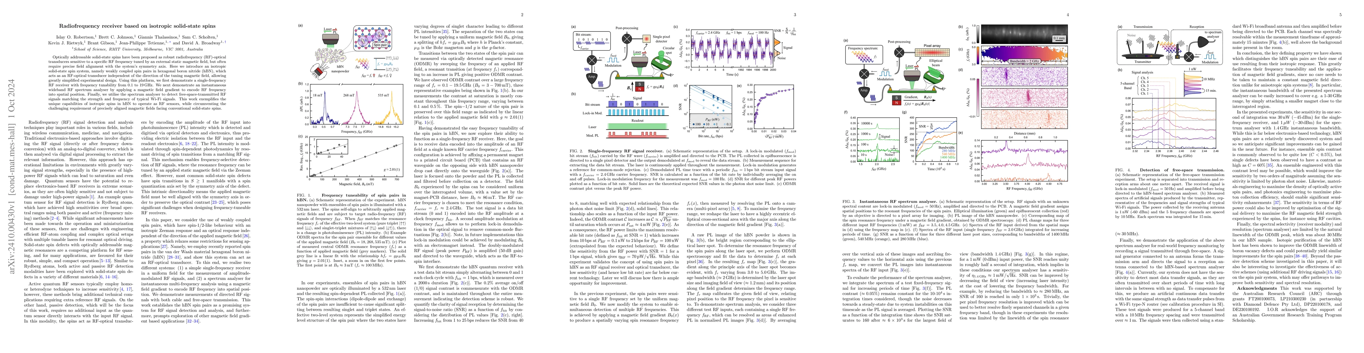
Optically addressable solid-state spins have been proposed as robust radiofrequency (RF)-optical transducers sensitive to a specific RF frequency tuned by an external static magnetic field, but often ...
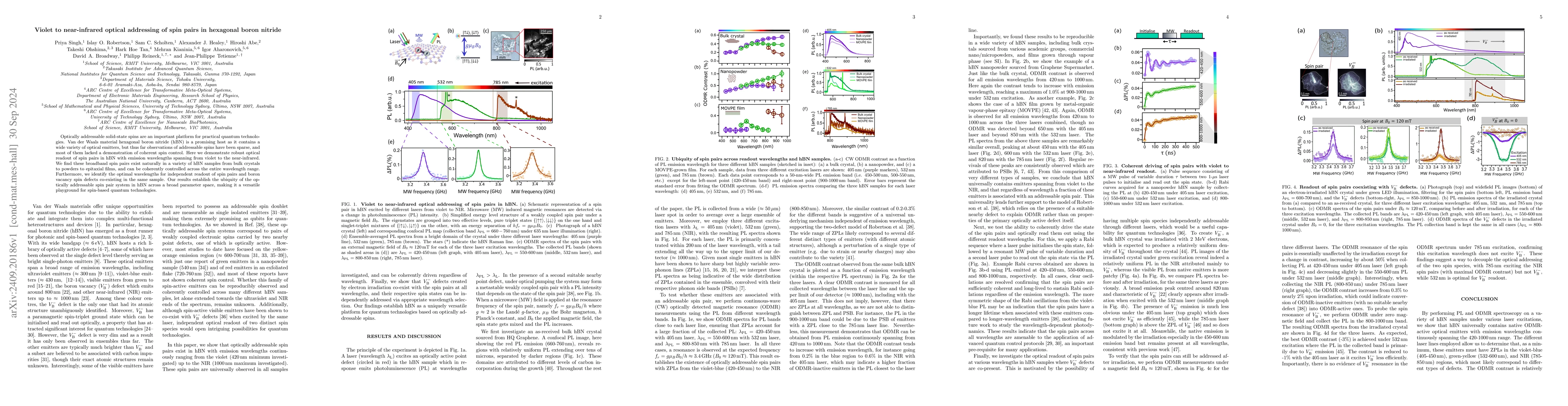
Optically addressable solid-state spins are an important platform for practical quantum technologies. Van der Waals material hexagonal boron nitride (hBN) is a promising host as it contains a wide var...
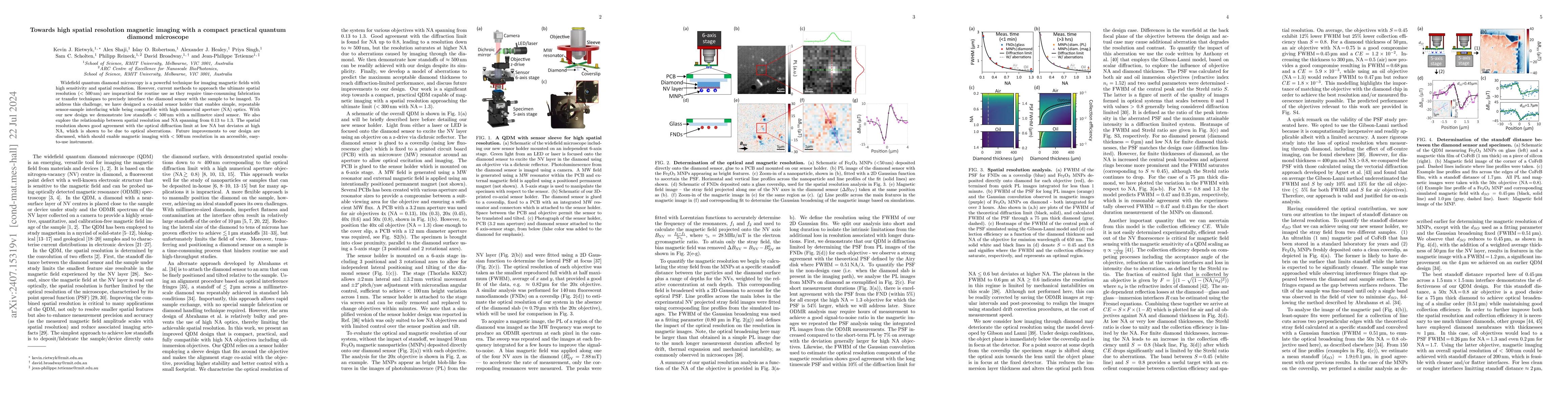
Widefield quantum diamond microscopy is a powerful technique for imaging magnetic fields with high sensitivity and spatial resolution. However, current methods to approach the ultimate spatial resolut...
Optically detected magnetic resonance (ODMR) has been observed from emitters in hexagonal boron nitride across a broad range of wavelengths, but so far an understanding of their microscopic structure ...
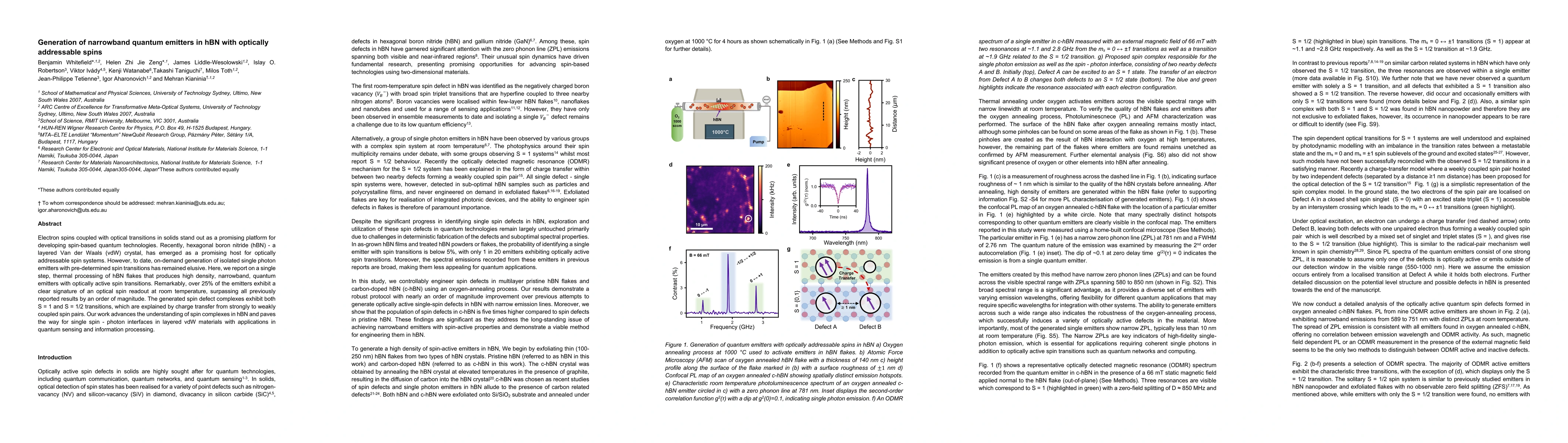
Electron spins coupled with optical transitions in solids stand out as a promising platform for developing spin-based quantum technologies. Recently, hexagonal boron nitride (hBN) - a layered Van der ...
Widefield magnetic imaging using ensembles of nitrogen-vacancy (NV) centres in diamond has emerged as a useful technique for studying the microscopic magnetic properties of materials. Thus far, this t...
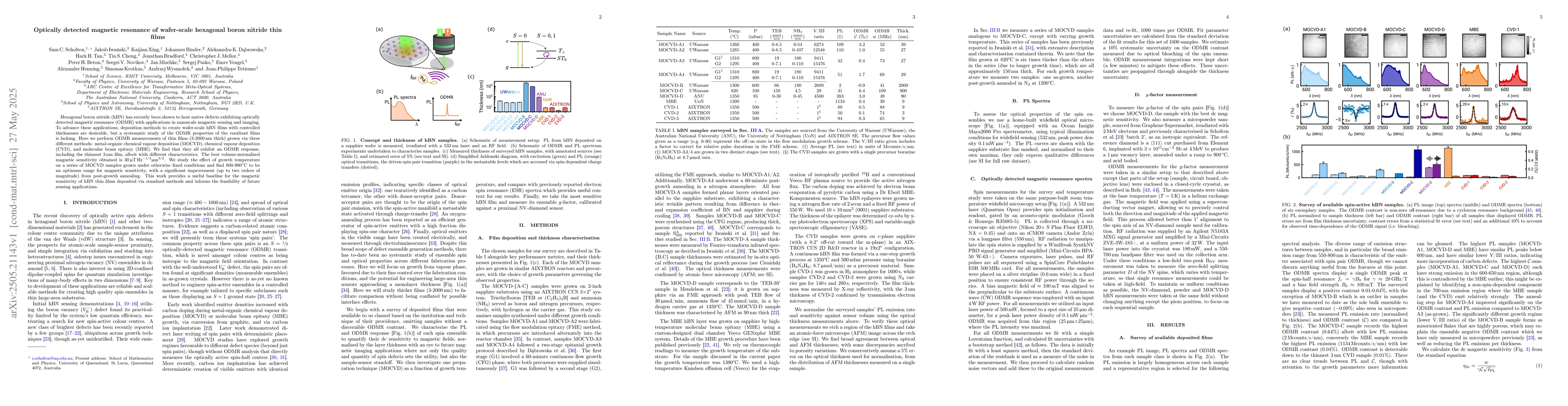
Hexagonal boron nitride (hBN) has recently been shown to host native defects exhibiting optically detected magnetic resonance (ODMR) with applications in nanoscale magnetic sensing and imaging. To adv...
The nitrogen-vacancy (NV) center is a photoluminescent defect in diamond that exists in different charge states, NV$^-$ and NV$^0$, that are sensitive to the NV's nanoscale environment. Here, we show ...
The nitrogen-vacancy (NV) center in diamond is emerging as a powerful tool for imaging magnetic and electric signals at the microscale and below. However, most imaging demonstrations thus far have rel...
Photoluminescent color centers in diamond and hexagonal boron nitride (hBN) are powerful nanoscale solid-state quantum sensors that are explored in a plethora of quantum technologies. Methods for inte...
The ability to modulate the photoluminescence (PL) of nanomaterials via spin-related effects is vital for many emerging quantum technologies, with nanoscale quantum sensing and imaging being particula...
Quantum emitters in hexagonal boron nitride (hBN) that exhibit optically detected magnetic resonance (ODMR) signatures have recently garnered significant attention as an emerging solid-state platform ...
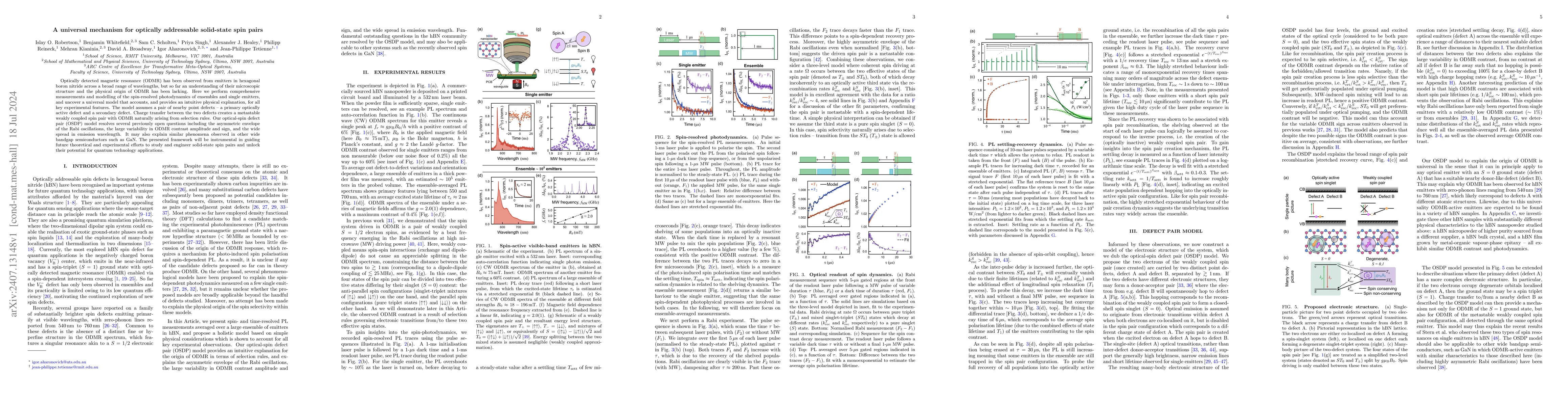
Optically addressable solid-state spin defects are essential platforms for quantum sensing and information processing. Recently, single spin defects with combined S = 1 and S = 1/2 spin transitions we...
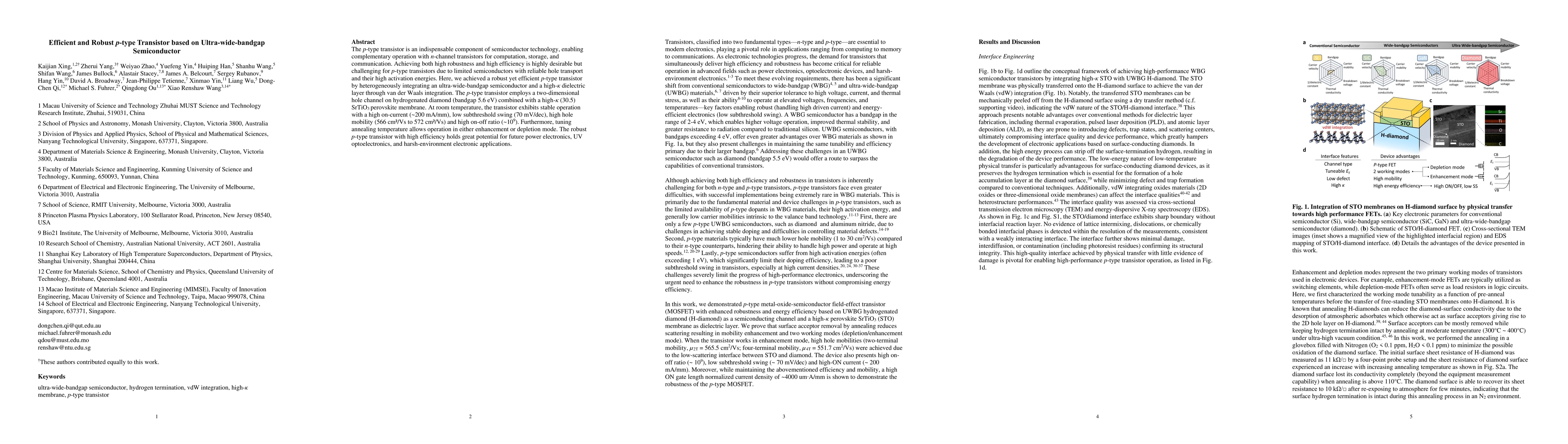
The p-type transistor is an indispensable component of semiconductor technology, enabling complementary operation with n-channel transistors for computation, storage, and communication. Achieving both...
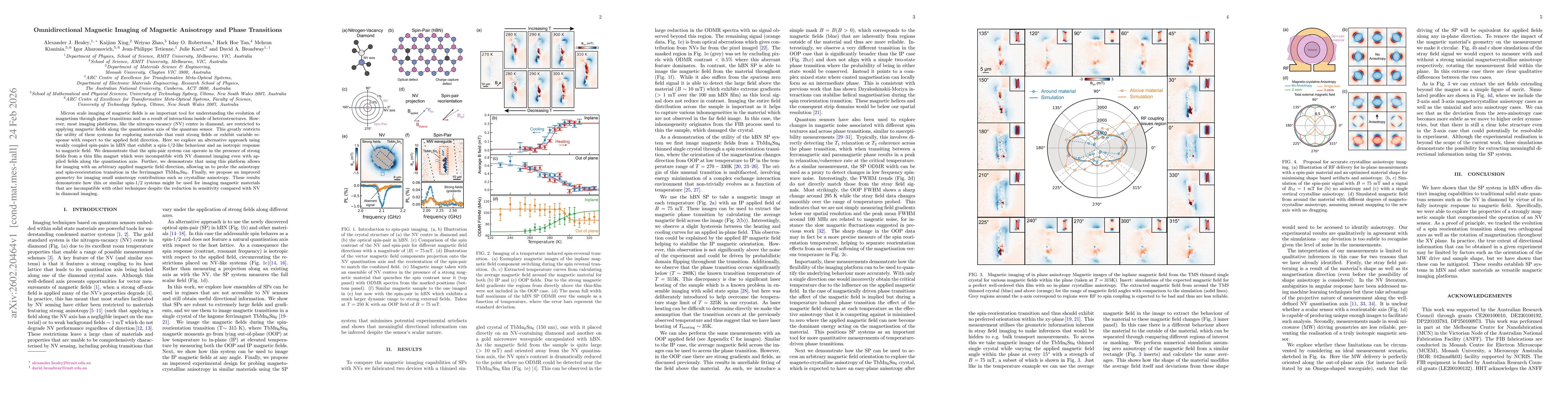
Micron scale imaging of magnetic fields is an important tool for understanding the evolution of magnetism through phase transitions and as a result of interactions inside of heterostructures. However,...
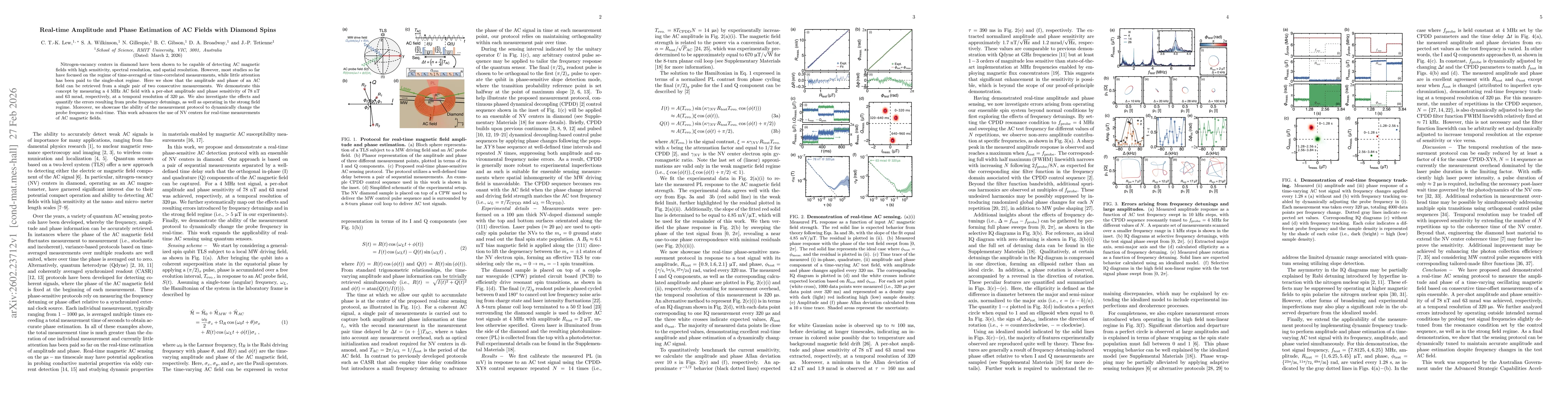
Nitrogen-vacancy centers in diamond have been shown to be capable of detecting AC magnetic fields with high sensitivity, spectral resolution, and spatial resolution. However, most studies so far have ...
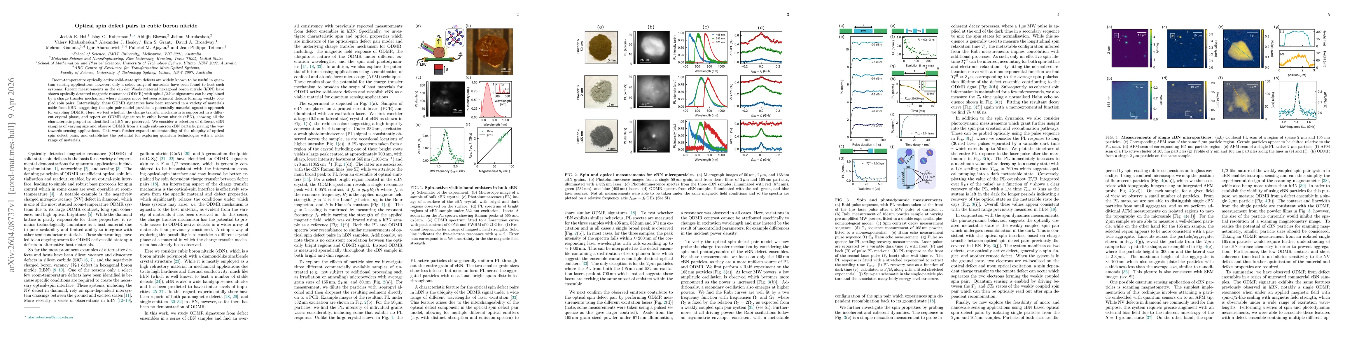
Room-temperature optically active solid-state spin defects are widely known to be useful in quantum sensing applications, however, only a select range of materials have been found to host such systems...
Nitrogen-vacancy (NV) centres in diamond can be used to detect radiofrequency (RF) signals through coupling of the RF magnetic field with the NV spins, combined with optical readout of the spin state....