Academic Profile
Statistics
Similar Authors
Papers on arXiv
The influence of chemical composition changes on the room temperature mechanical proper-ties in the C15 CaAl2 Laves phase were investigated in two off-stoichiometric compositions with 5.7 at.-% Mg a...
The proximity effect at a highly transparent interface of an s-wave superconductor (S) and a topological insulator (TI) provides a promising platform to create Majorana zero modes in artificially de...
Two-dimensional (2D) materials are popular candidates for emerging nanoscale devices, including memristors. Resistive switching (RS) in such 2D material memristors has been attributed to the formati...
The two-dimensional (2D) insulating material hexagonal boron nitride (h BN) has attracted much attention as the active medium in memristive devices due to its favorable physical properties, among ot...
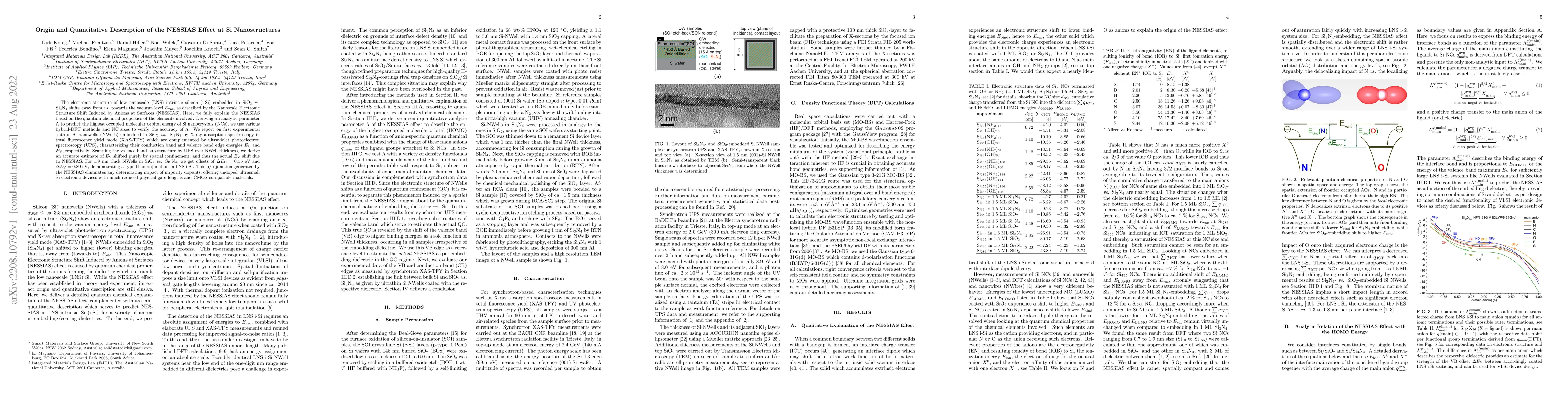
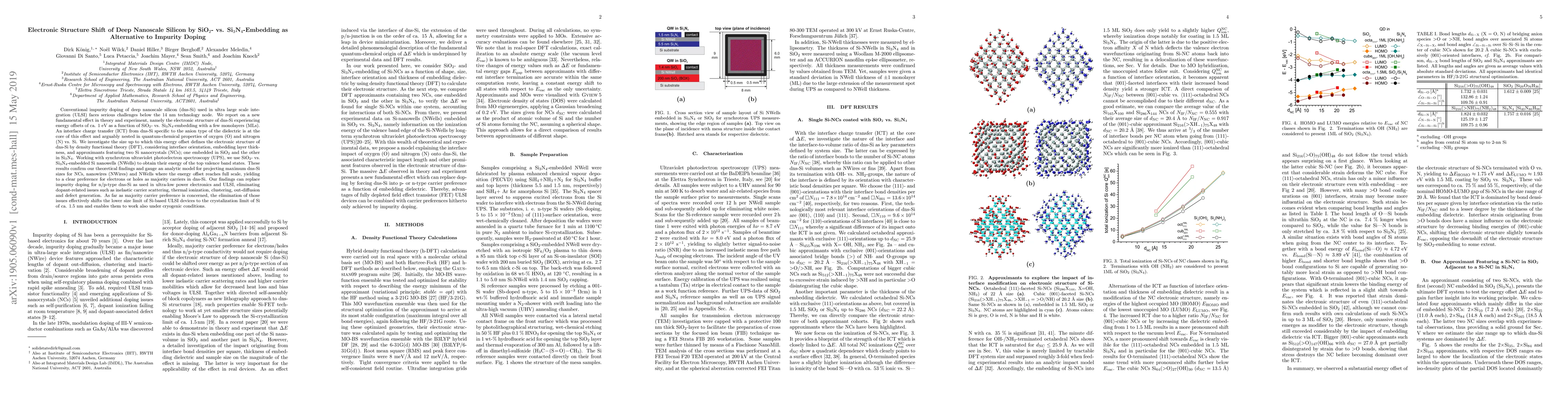
The electronic structure of low nanoscale (LNS) intrinsic silicon (i-Si) embedded in SiO2 vs. Si3N4 shifts away from vs. towards the vacuum level Evac, as described by the Nanoscale Electronic Struc...
When a topological insulator is made into a nanowire, the interplay between topology and size quantization gives rise to peculiar one-dimensional states whose energy dispersion can be manipulated by...
Platinum diselenide (PtSe${_2}$) is a two-dimensional (2D) material with outstanding electronic and piezoresistive properties. The material can be grown at low temperatures in a scalable manner whic...
The scientific and technological exploration of artificially designed three-dimensional magnetic nanostructures opens the path to exciting novel physical phenomena, originating from the increased co...
Spontaneous polarization is essential for ferroelectric functionality in non-centrosymmetric crystals. High-integration-density ferroelectric devices require the stabilization of ferroelectric polar...
Conventional impurity doping of deep nanoscale silicon (dns-Si) used in ultra large scale integration (ULSI) faces serious challenges below the 14 nm technology node. We report on a new fundamental ...
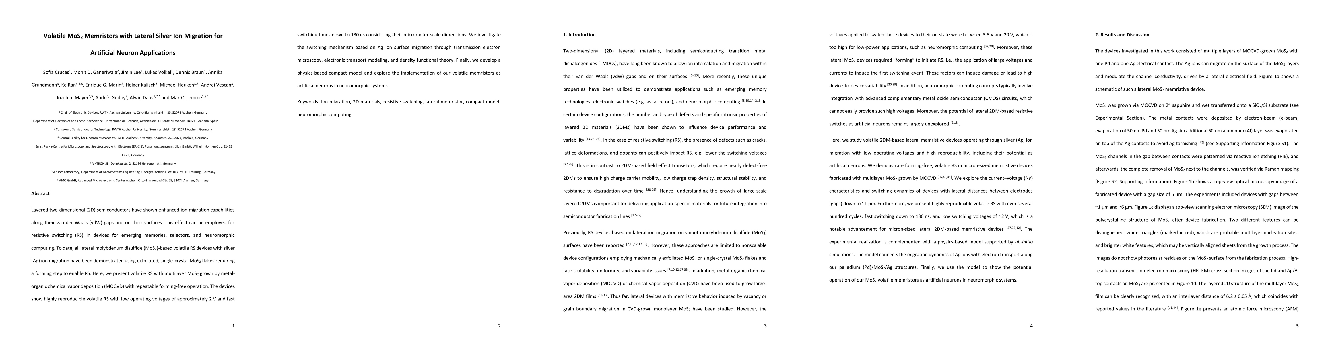
Layered two-dimensional (2D) semiconductors have shown enhanced ion migration capabilities along their van der Waals (vdW) gaps and on their surfaces. This effect can be employed for resistive switchi...
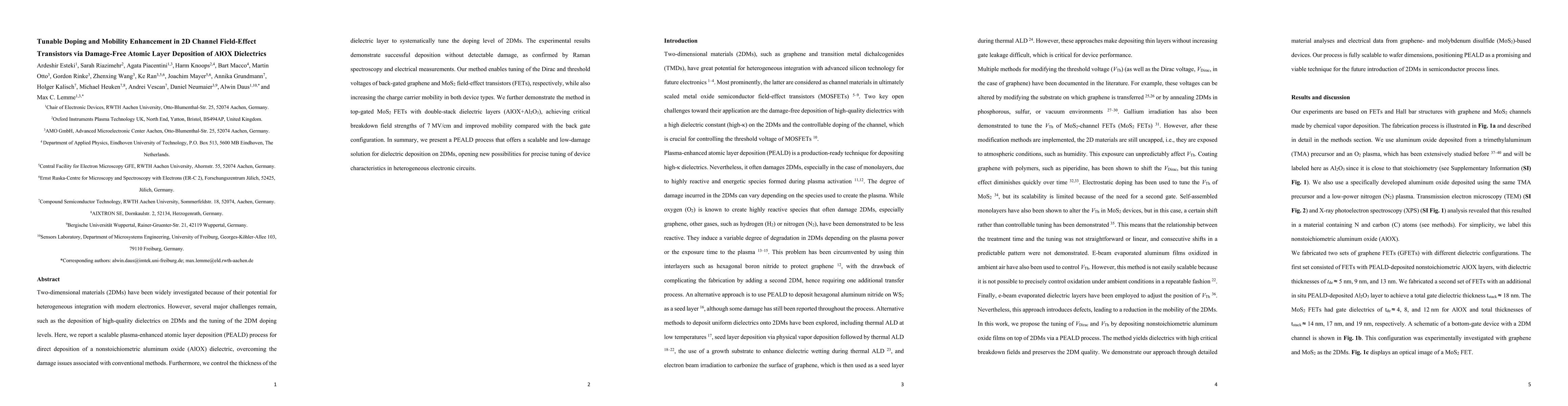
Two-dimensional materials (2DMs) have been widely investigated because of their potential for heterogeneous integration with modern electronics. However, several major challenges remain, such as the d...
Threshold switching (TS) is a phenomenon where non-permanent changes in electrical resistance of a two-terminal device can be controlled by modulating the voltage bias. TS based on silver (Ag) conduct...
Advanced operando transmission electron microscopy (TEM) techniques enable the observation of nanoscale phenomena in electrical devices during operation. They can be used to study the switching mechan...
Developing electronic devices capable of emulating biological functions is essential for advancing brain-inspired computation paradigms such as neuromorphic computing. In recent years, two-dimensional...
Memristors based on two-dimensional materials (2DMs) have garnered significant attention due to their fast resistive switching (RS) behavior and atomic-level thickness, which enables low power consump...
Layered two-dimensional (2D) materials provide unique structural features, such as physical gaps between their layers that are only connected through van der Waals (vdW) forces. These vdW gaps can gui...
Lithium (Li) plating on graphite is a significant degradation mechanism in Li-ion batteries. While numerous experimental techniques have been used to study Li plating in laboratory cells, investigatio...