Academic Profile
Statistics
Similar Authors
Papers on arXiv
Achieving localized light emission from monolayer two-dimensional (2D) transition metal dichalcogenides (TMDs) embedded in the matrix of another TMD has been theoretically proposed but not experimen...
Ferroelectric field-effect transistors (FeFET) with two-dimensional (2D) semiconductor channels are promising low-power, embedded non-volatile memory (NVM) candidates for next-generation in-memory c...
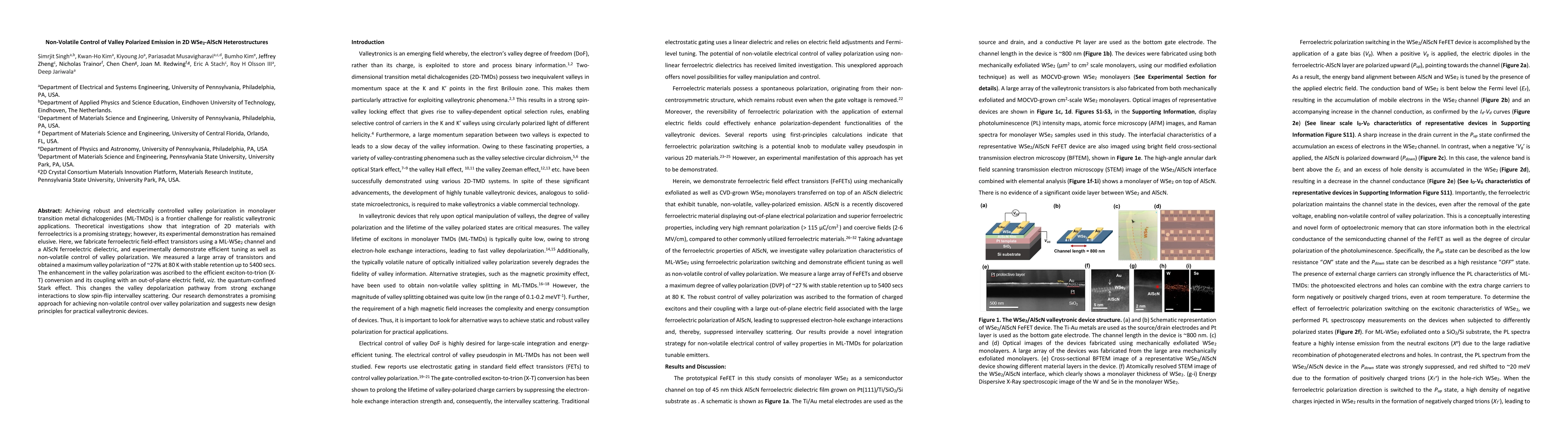
Achieving robust and electrically controlled valley polarization in monolayer transition metal dichalcogenides (ML-TMDs) is a frontier challenge for realistic valleytronic applications. Theoretical ...
Two-dimensional (2D) semiconductors are promising candidates for optoelectronic application and quantum information processes due to their inherent out-of-plane 2D confinement. In addition, they off...
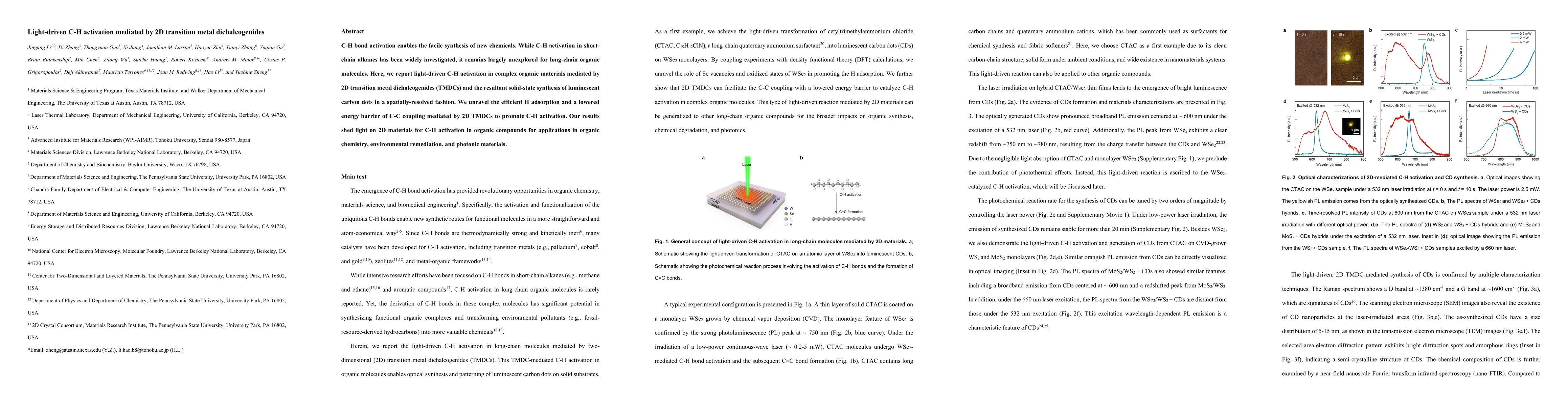
C-H bond activation enables the facile synthesis of new chemicals. While C-H activation in short-chain alkanes has been widely investigated, it remains largely unexplored for long-chain organic mole...
Two-dimensional chalcogenide semiconductors have recently emerged as a host material for quantum emitters of single photons. While several reports on defect and strain-induced single photon emission...
Two-dimensional (2D) crystals have renewed opportunities in design and assembly of artificial lattices without the constraints of epitaxy. However, the lack of thickness control in exfoliated van de...
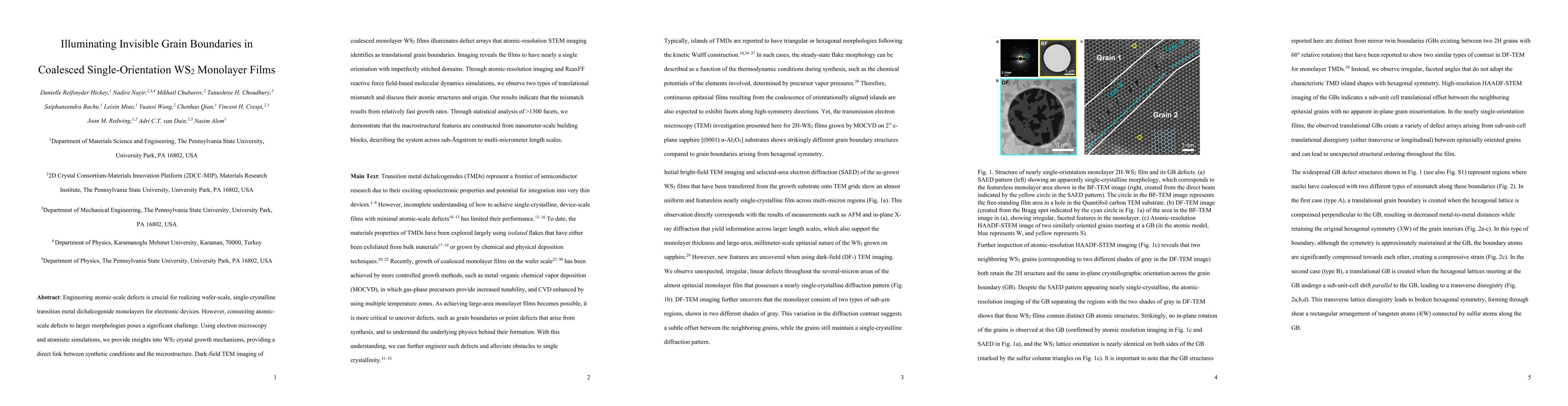
Engineering atomic-scale defects is crucial for realizing wafer-scale, single-crystalline transition metal dichalcogenide monolayers for electronic devices. However, connecting atomic-scale defects ...
Realization of wafer-scale single-crystal films of transition metal dichalcogenides (TMDs) such as tungsten sulfide requires epitaxial growth and coalescence of oriented domains to form a continuous...
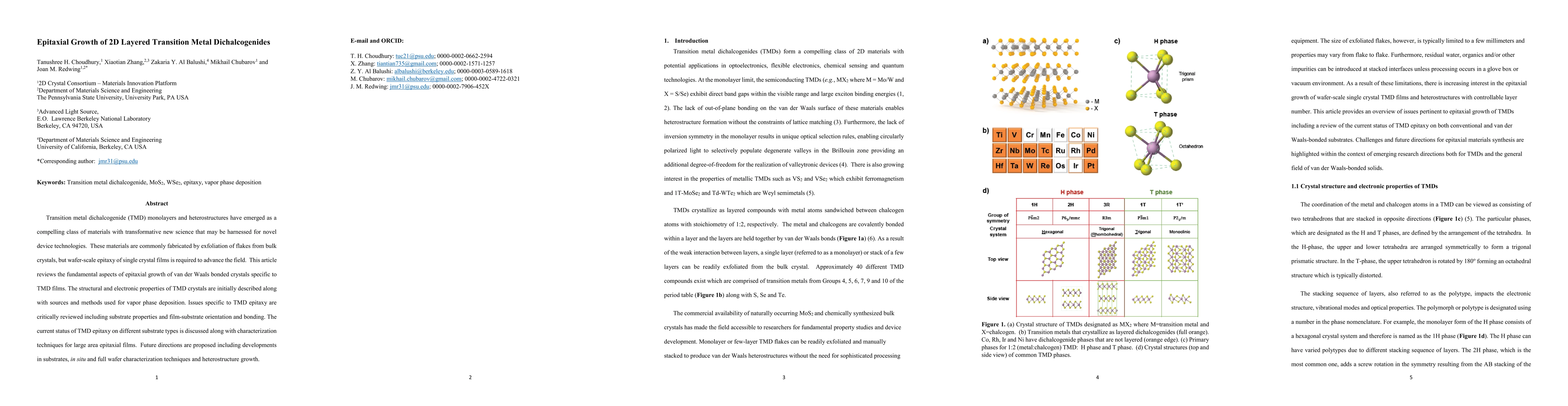
Transition metal dichalcogenide (TMD) monolayers and heterostructures have emerged as a compelling class of materials with transformative new science that may be harnessed for novel device technolog...
Broadband absorption in the visible spectrum is essential in optoelectronic applications that involve power conversion such as photovoltaics and photocatalysis. Most ultrathin broadband absorbers use ...
The growth and characterization of materials using empirical optimization typically requires a significant amount of expert time, experience, and resources. Several complementary characterization meth...
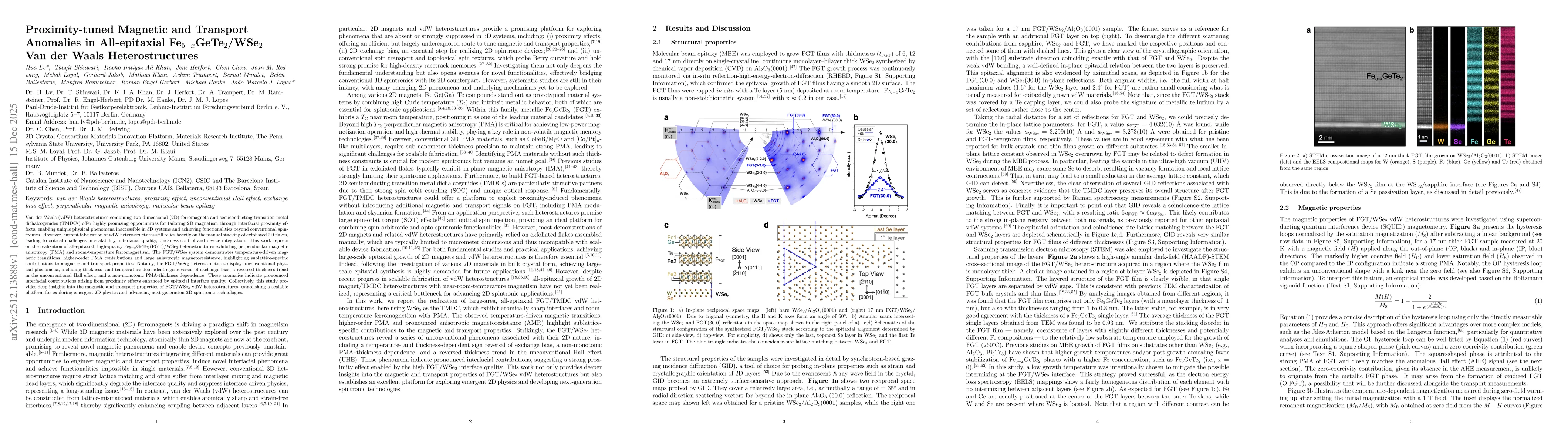
Van der Waals (vdW) heterostructures combining two-dimensional (2D) ferromagnets and semiconducting transition-metal dichalcogenides (TMDCs) offer highly promising opportunities for tailoring 2D magne...
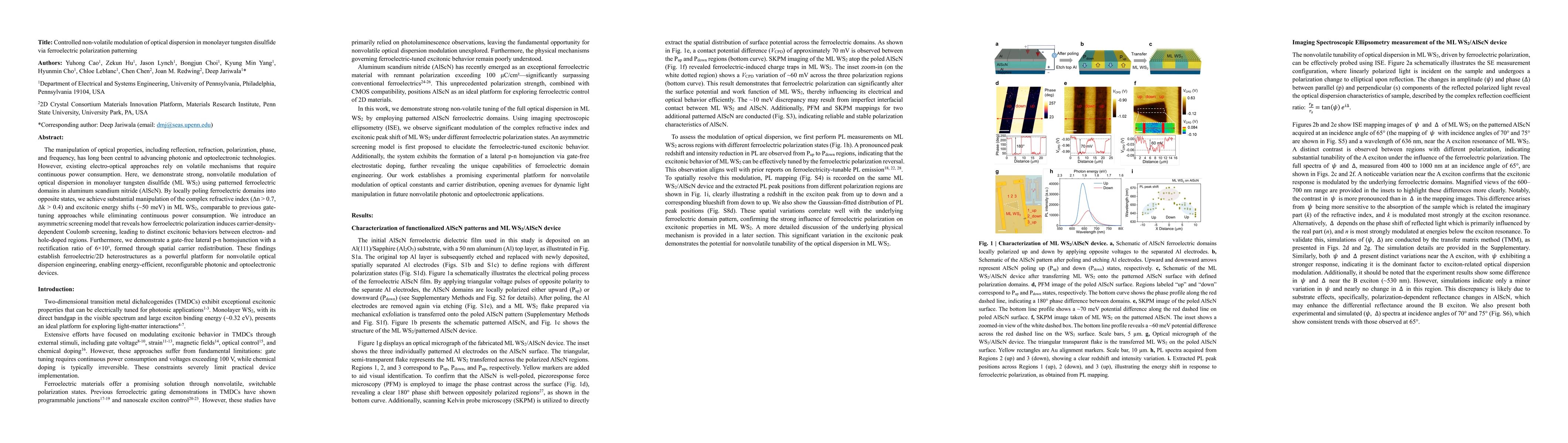
The manipulation of optical properties, including reflection, refraction, polarization, phase, and frequency, has long been central to advancing photonic and optoelectronic technologies. However, exis...
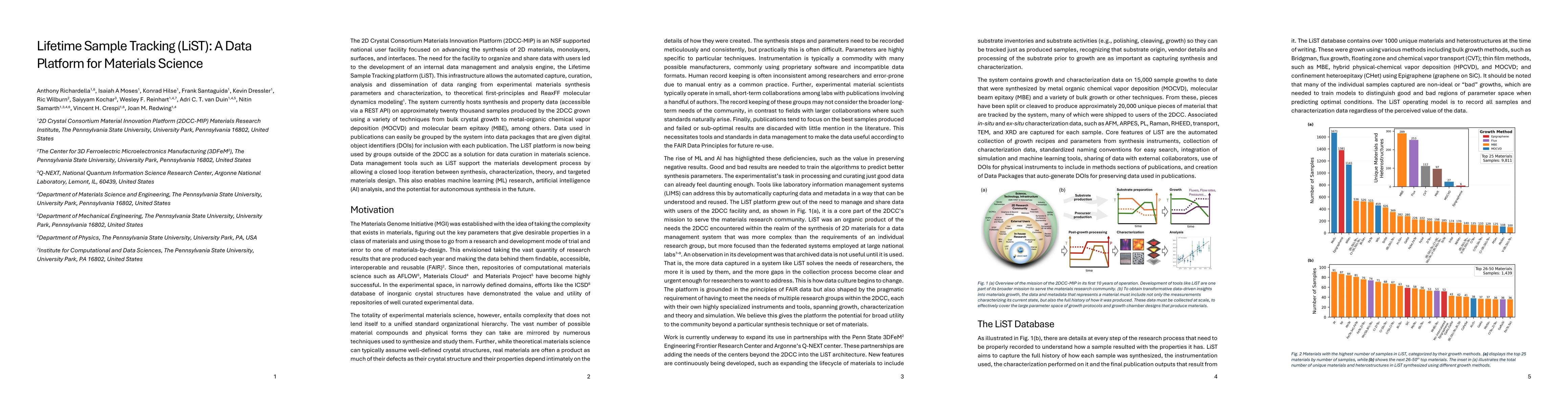
The 2D Crystal Consortium Materials Innovation Platform (2DCC-MIP) is an NSF supported national user facility focused on advancing the synthesis of 2D materials, monolayers, surfaces, and interfaces. ...