ArxivLens
J
Researcher

Johannes Jobst

7 papers on arXiv

7 arXiv Papers
7 Total Publications
Profile

Academic Profile

Name M. Jobst
Total Papers 7
Scholar Profile View on Semantic Scholar
Metrics

Statistics

7 arXiv Papers
7 Total Publications
Publications

Papers on arXiv

Thumbnail for Stacking domain morphology in epitaxial graphene on silicon carbide
arXiv
Stacking domain morphology in epitaxial graphene on silicon carbide

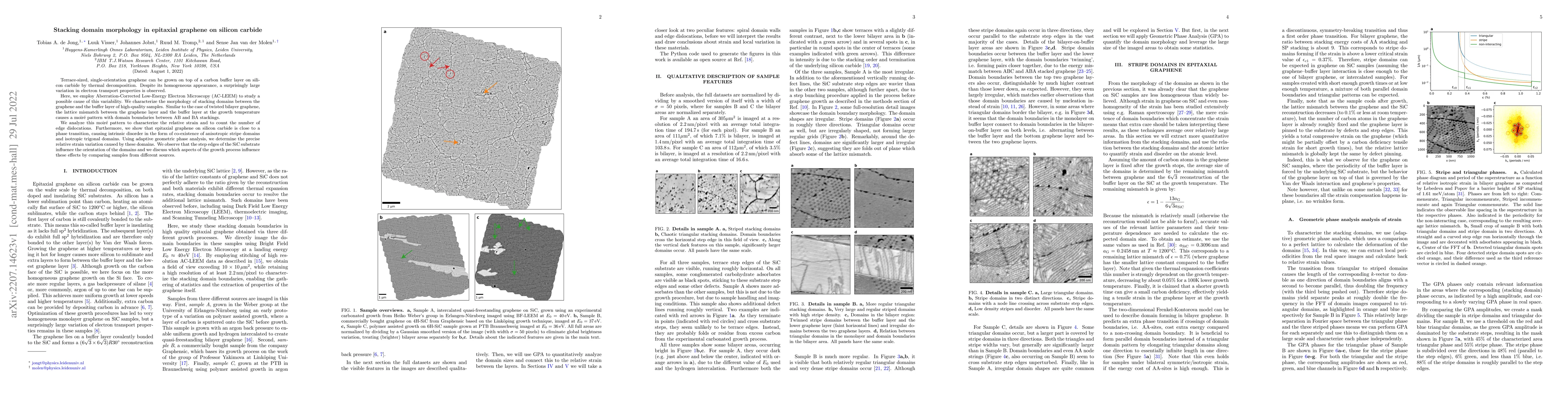
Terrace-sized, single-orientation graphene can be grown on top of a carbon buffer layer on silicon carbide by thermal decomposition. Despite its homogeneous appearance, a surprisingly large variatio...

Thumbnail for Low-Energy Electron Microscopy contrast of stacking boundaries:
  comparing twisted few-layer graphene and strained epitaxial graphene on
  silicon carbide
arXiv
Low-Energy Electron Microscopy contrast of stacking boundaries: comparing twisted few-layer graphene and strained epitaxial graphene on silicon carbide

Stacking domain boundaries occur in Van der Waals heterostacks whenever there is a twist angle or lattice mismatch between subsequent layers. Not only can these domain boundaries host topological ed...

Thumbnail for Direct evidence for flat bands in twisted bilayer graphene from
  nano-ARPES
arXiv
Direct evidence for flat bands in twisted bilayer graphene from nano-ARPES

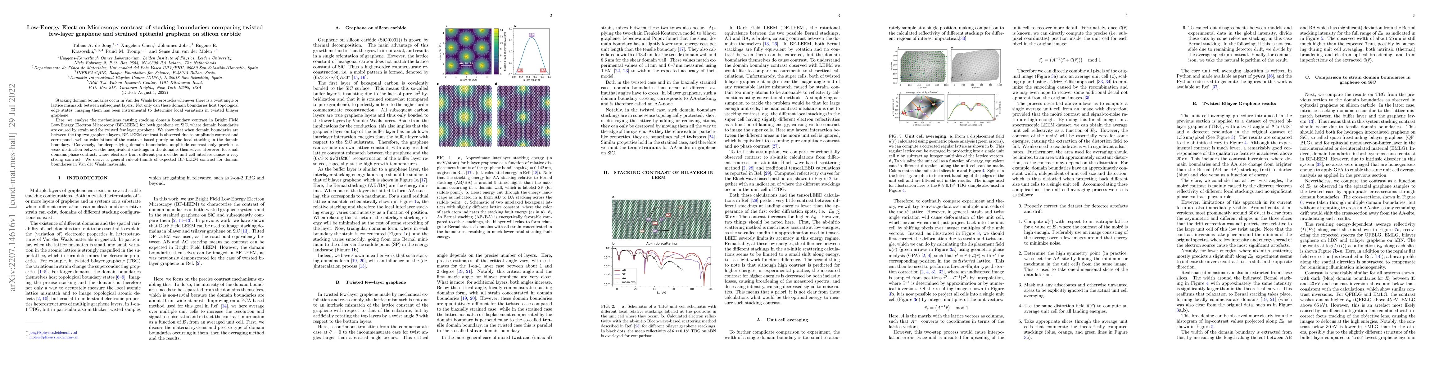
Transport experiments in twisted bilayer graphene revealed multiple superconducting domes separated by correlated insulating states. These properties are generally associated with strongly correlate...

Thumbnail for Growing a LaAlO3/SrTiO3 heterostructure on Ca2Nb3O10 nanosheets
arXiv
Growing a LaAlO3/SrTiO3 heterostructure on Ca2Nb3O10 nanosheets

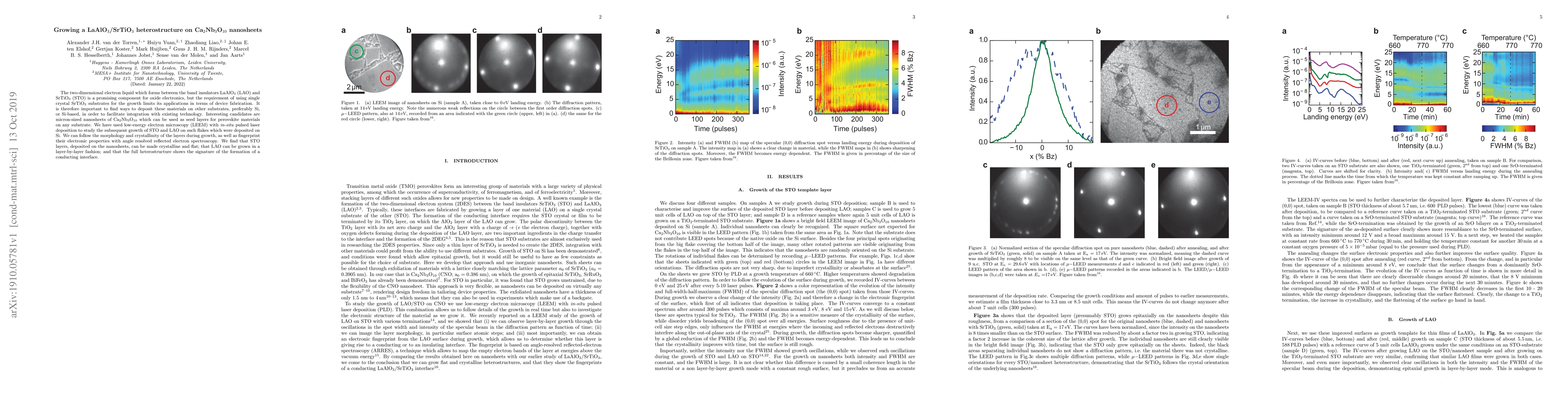
The two-dimensional electron liquid which forms between the band insulators LaAlO3 (LAO) and SrTiO3 (STO) is a promising component for oxide electronics, but the requirement of using single crystal ...

Thumbnail for Low-Energy Electron Potentiometry
arXiv
Low-Energy Electron Potentiometry

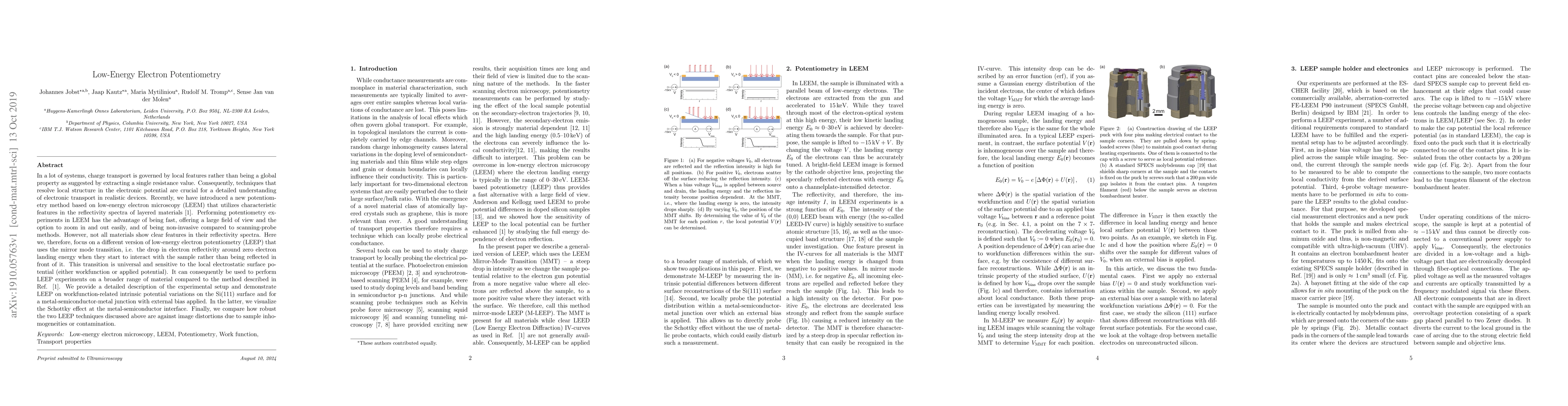
In a lot of systems, charge transport is governed by local features rather than being a global property as suggested by extracting a single resistance value. Consequently, techniques that resolve lo...

Thumbnail for Patterning Sn-based EUV resists with low-energy electrons
arXiv
Patterning Sn-based EUV resists with low-energy electrons

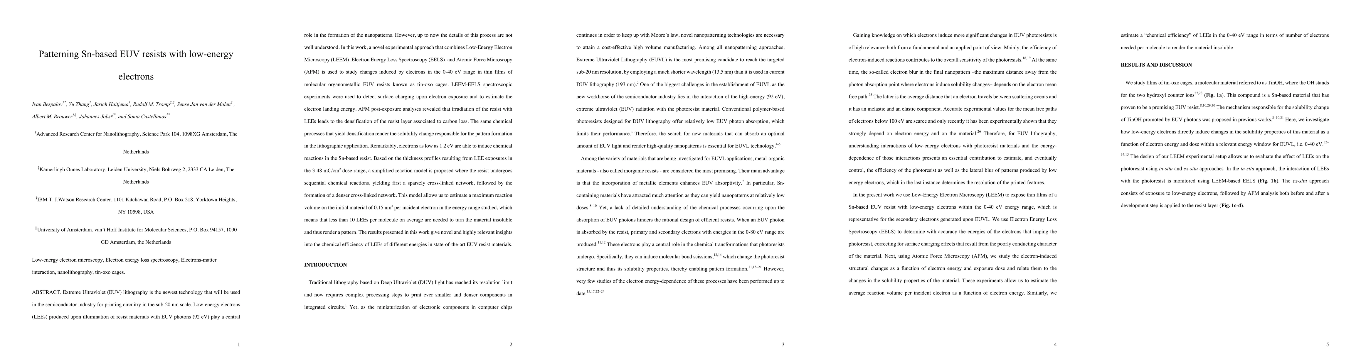
Extreme Ultraviolet (EUV) lithography is the newest technology that will be used in the semiconductor industry for printing circuitry in the sub-20 nm scale. Low-energy electrons (LEEs) produced upo...

Thumbnail for Quantitative analysis of spectroscopic Low Energy Electron Microscopy
  data: High-dynamic range imaging, drift correction and cluster analysis
arXiv
Quantitative analysis of spectroscopic Low Energy Electron Microscopy data: High-dynamic range imaging, drift correction and cluster analysis

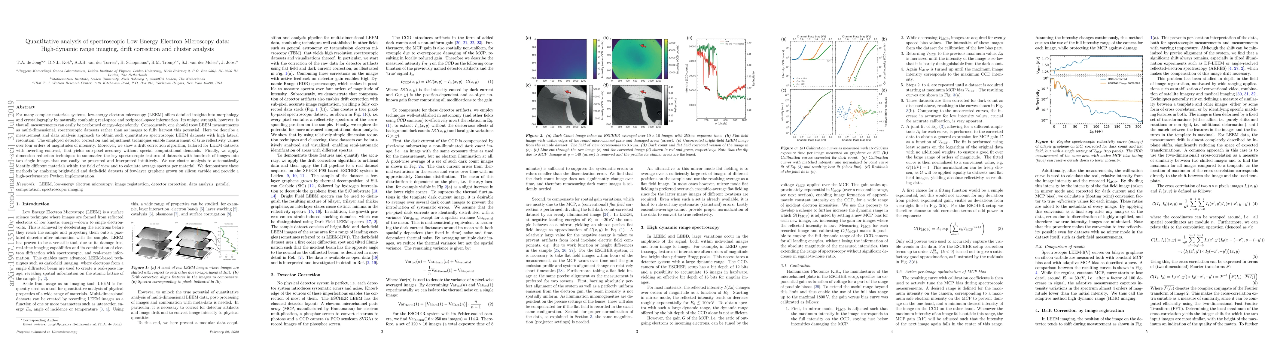
For many complex materials systems, low-energy electron microscopy (LEEM) offers detailed insights into morphology and crystallography by naturally combining real-space and reciprocal-space informat...

This website uses cookies to ensure you get the best experience. Learn more