Jonas Lähnemann

28 papers on arXiv

Academic Profile

Name: J. Lähnemann
Total Papers: 96

Statistics

arXiv Papers 28
Total Publications 96

Papers on arXiv

Thumbnail for Uniform large-area surface patterning achieved by metal dewetting for
  the top-down fabrication of GaN nanowire ensembles

Uniform large-area surface patterning achieved by metal dewetting for the top-down fabrication of GaN nanowire ensembles

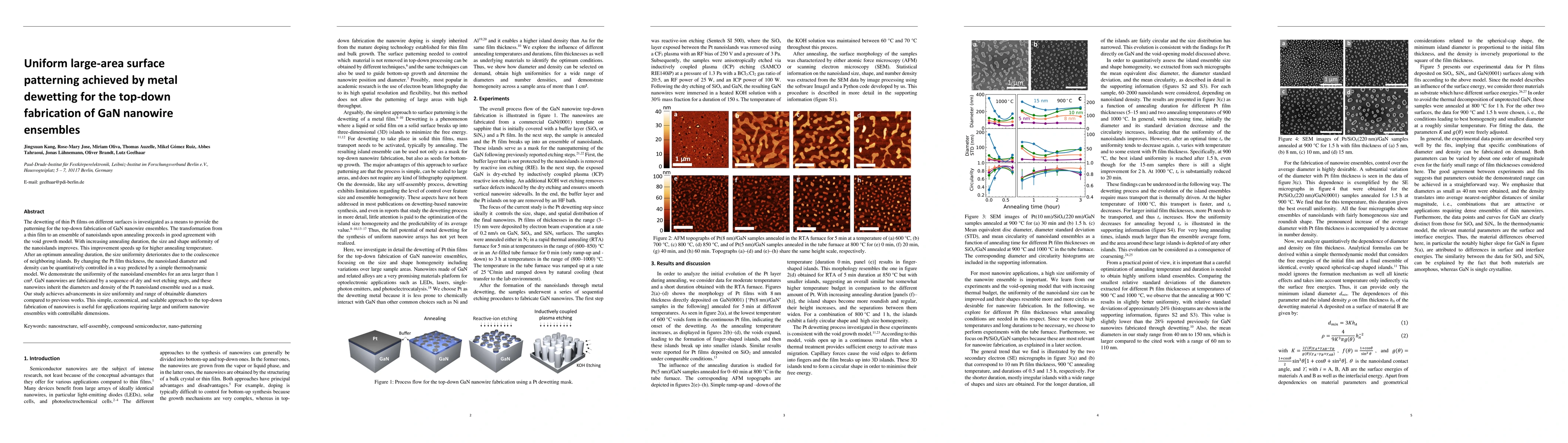
The dewetting of thin Pt films on different surfaces is investigated as a means to provide the patterning for the top-down fabrication of GaN nanowire ensembles. The transformation from a thin film ...

Thumbnail for ScN/GaN($1\bar{1}00$): a new platform for the epitaxy of twin-free
  metal-semiconductor heterostructures

ScN/GaN($1\bar{1}00$): a new platform for the epitaxy of twin-free metal-semiconductor heterostructures

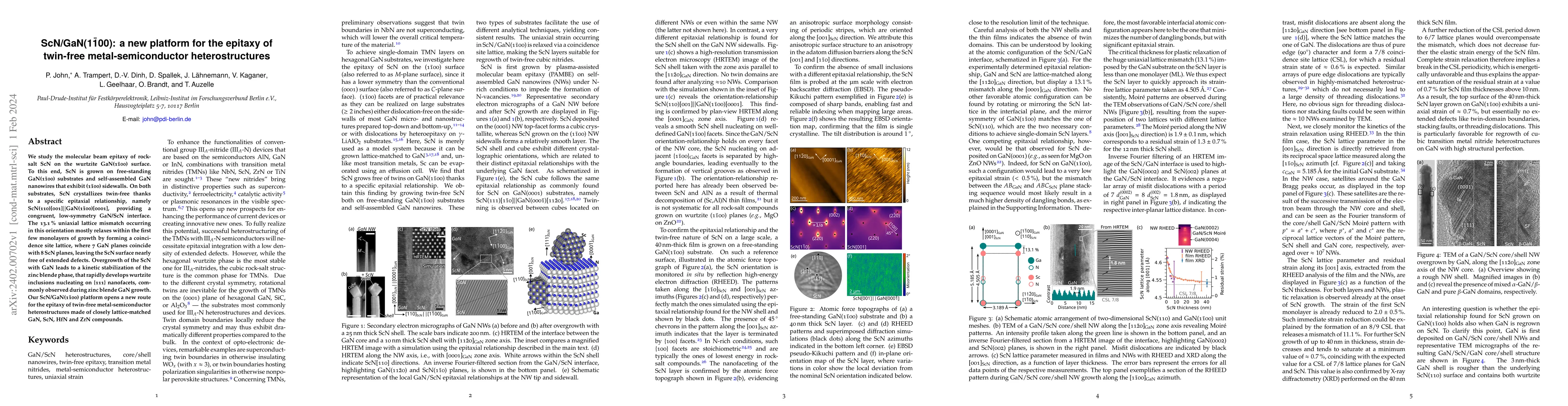
We study the molecular beam epitaxy of rock-salt ScN on the wurtzite GaN($1\bar{1}00$) surface. To this end, ScN is grown on free-standing GaN($1\bar{1}00$) substrates and self-assembled GaN nanowir...

Thumbnail for Composition and optical properties of (In,Ga)As nanowires grown by
  group-III-assisted molecular beam epitaxy

Composition and optical properties of (In,Ga)As nanowires grown by group-III-assisted molecular beam epitaxy

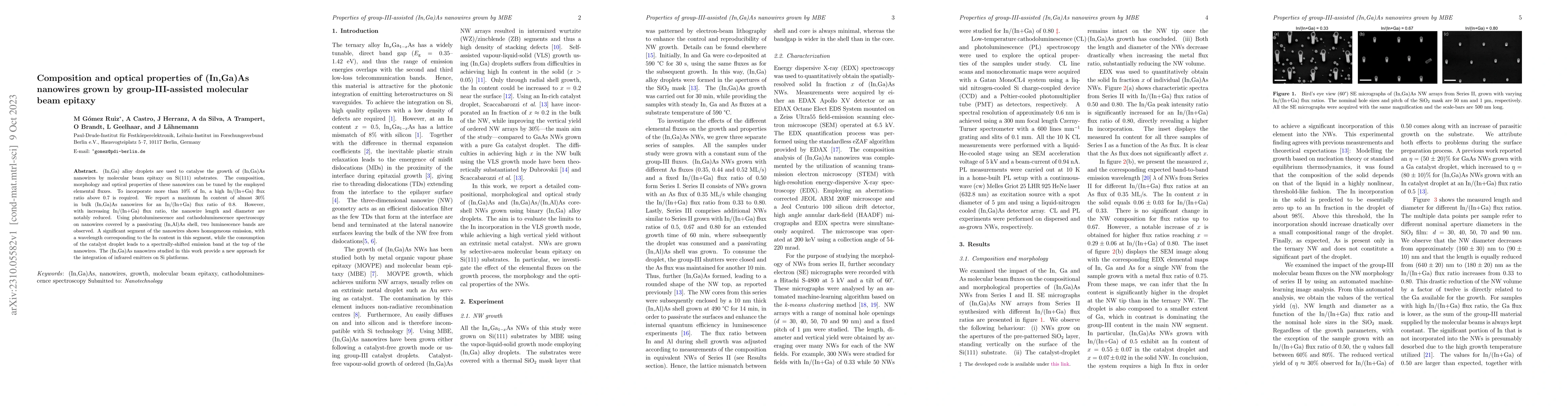
(In,Ga) alloy droplets are used to catalyse the growth of (In,Ga)As nanowires by molecular beam epitaxy on Si(111) substrates. The composition, morphology and optical properties of these nanowires c...

Thumbnail for Sequential directional deposition of one-sided (In,Ga)N shells on GaN
  nanowires by molecular beam epitaxy

Sequential directional deposition of one-sided (In,Ga)N shells on GaN nanowires by molecular beam epitaxy

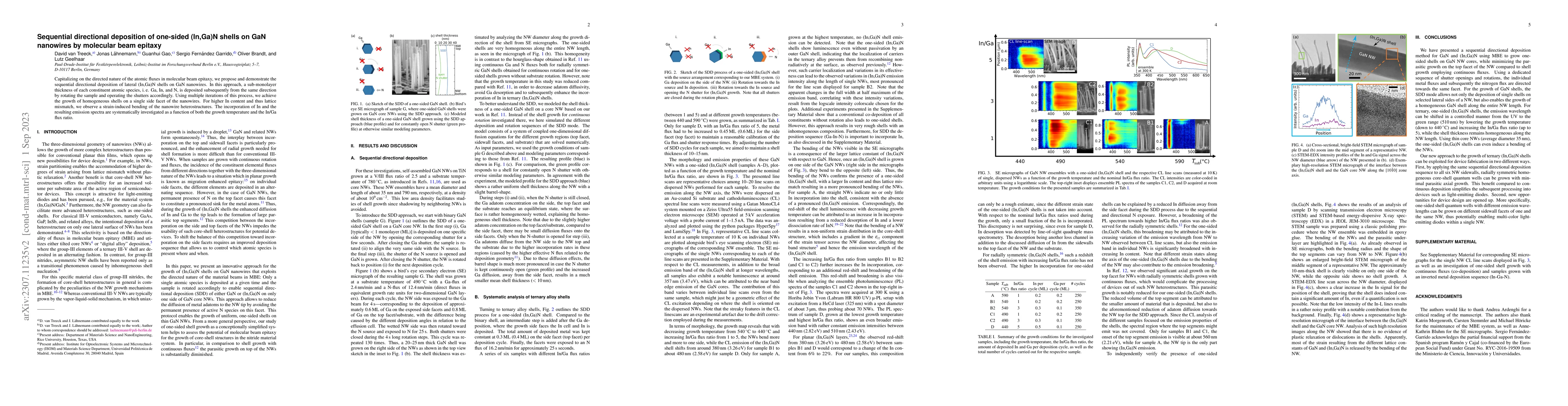
Capitalizing on the directed nature of the atomic fluxes in molecular beam epitaxy, we propose and demonstrate the sequential directional deposition of lateral (In,Ga)N shells on GaN nanowires. In t...

Thumbnail for Growth mechanisms in molecular beam epitaxy for GaN-(In,Ga)N core-shell
  nanowires emitting in the green spectral range

Growth mechanisms in molecular beam epitaxy for GaN-(In,Ga)N core-shell nanowires emitting in the green spectral range

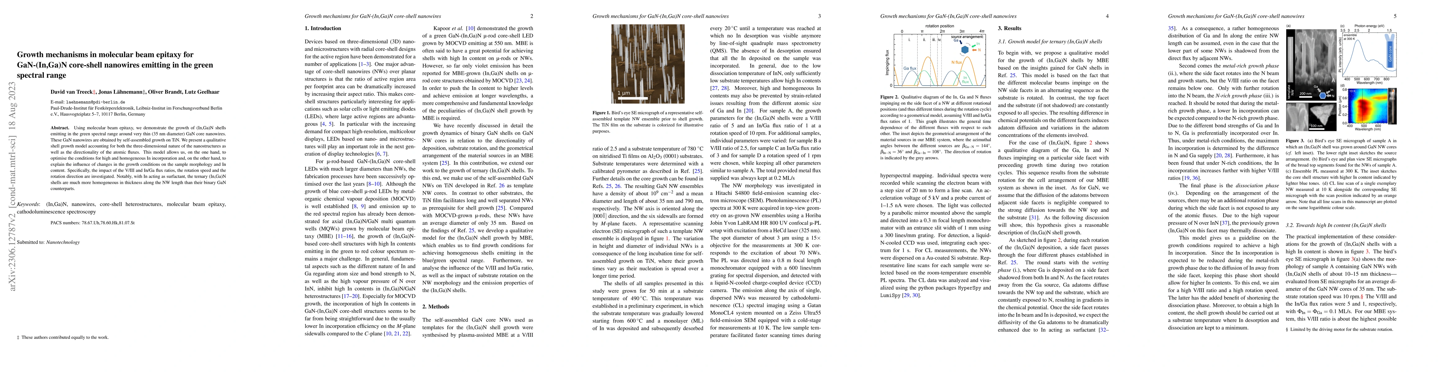
Using molecular beam epitaxy, we demonstrate the growth of (In,Ga)N shells emitting in the green spectral range around very thin (35 nm diameter) GaN core nanowires. These GaN nanowires are obtained...

Thumbnail for Optical properties of ScN layers grown on Al$_{2}$O$_{3}$(0001) by
  plasma-assisted molecular beam epitaxy

Optical properties of ScN layers grown on Al$_{2}$O$_{3}$(0001) by plasma-assisted molecular beam epitaxy

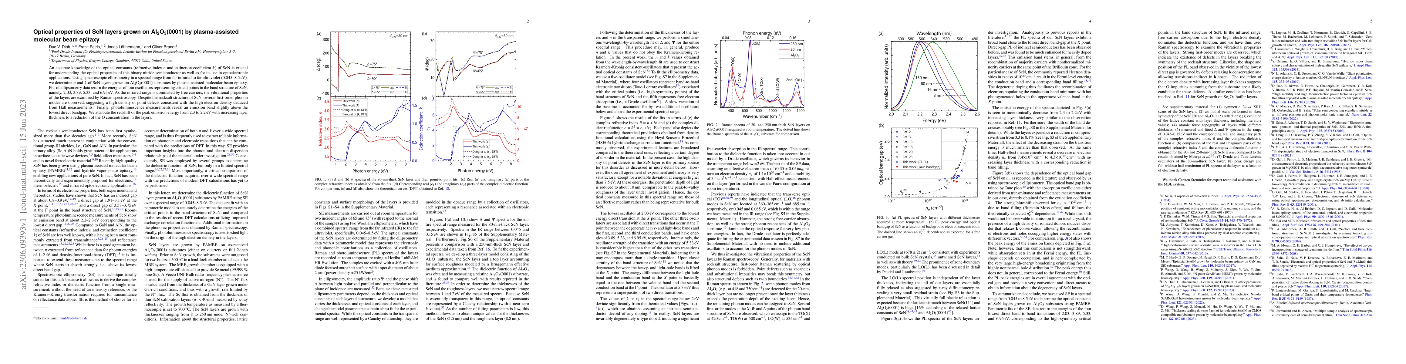
An accurate knowledge of the optical constants (refractive index $n$ and extinction coefficient $k$) of ScN is crucial for understanding the optical properties of this binary nitride semiconductor a...

Thumbnail for Growth kinetics and substrate stability during high-temperature
  molecular beam epitaxy of AlN nanowires

Growth kinetics and substrate stability during high-temperature molecular beam epitaxy of AlN nanowires

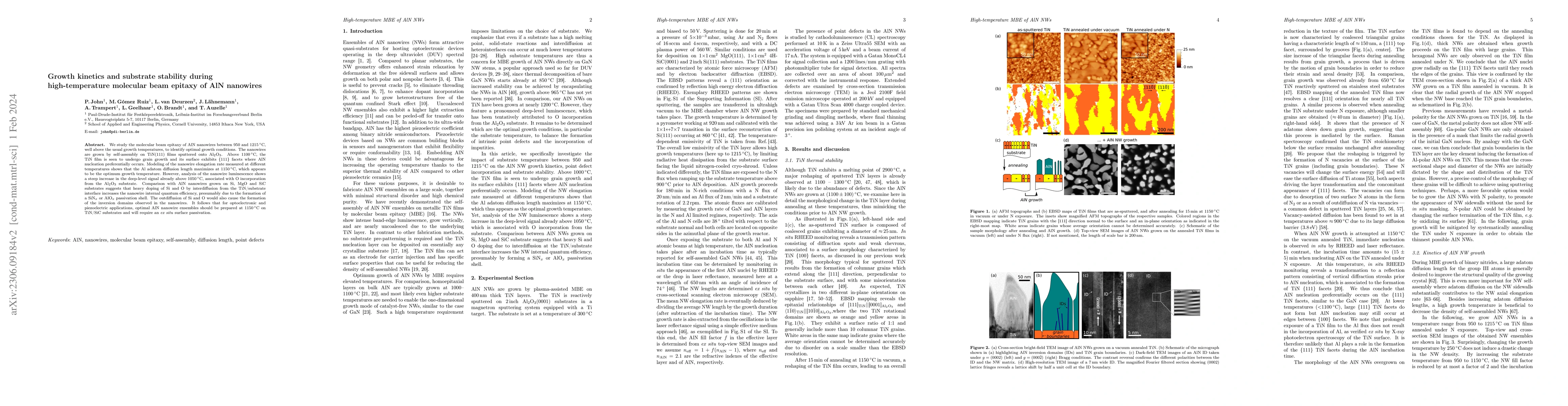
We study the molecular beam epitaxy of AlN nanowires between 950 and 1215 {\deg}C, well above the usual growth temperatures, to identify optimal growth conditions. The nanowires are grown by self-as...

Thumbnail for Excitonic and deep-level emission from N- and Al-polar homoepitaxial AlN
  grown by molecular beam epitaxy

Excitonic and deep-level emission from N- and Al-polar homoepitaxial AlN grown by molecular beam epitaxy

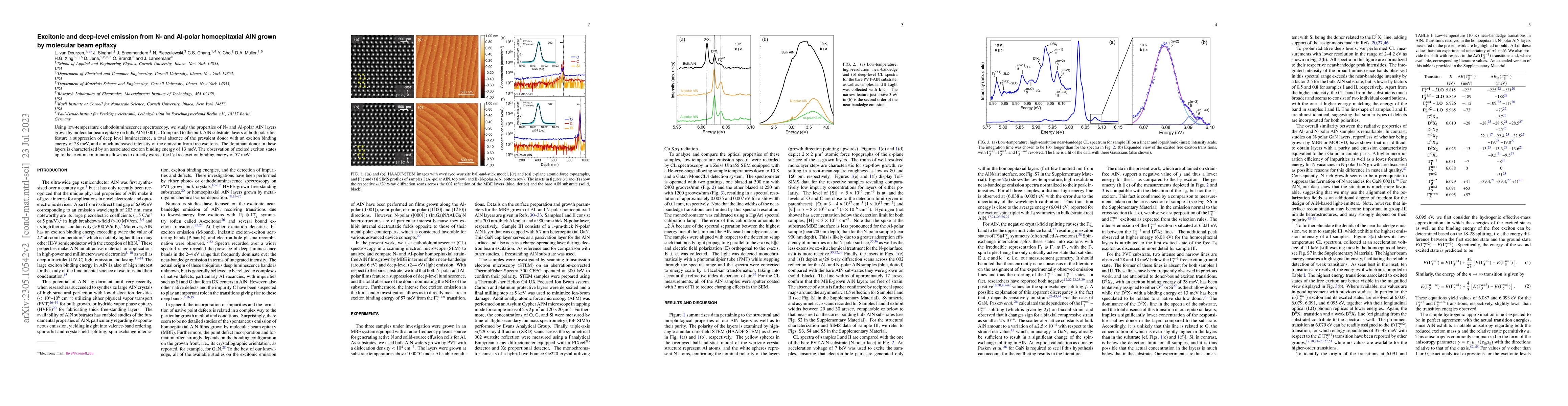
Using low-temperature cathodoluminescence spectroscopy, we study the properties of N- and Al-polar AlN layers grown by molecular beam epitaxy on bulk AlN{0001}. Compared to the bulk AlN substrate, l...

Thumbnail for Acceptor and compensating donor doping of single crystalline SnO (001)
  films grown by molecular beam epitaxy and its perspectives for
  optoelectronics and gas-sensing

Acceptor and compensating donor doping of single crystalline SnO (001) films grown by molecular beam epitaxy and its perspectives for optoelectronics and gas-sensing

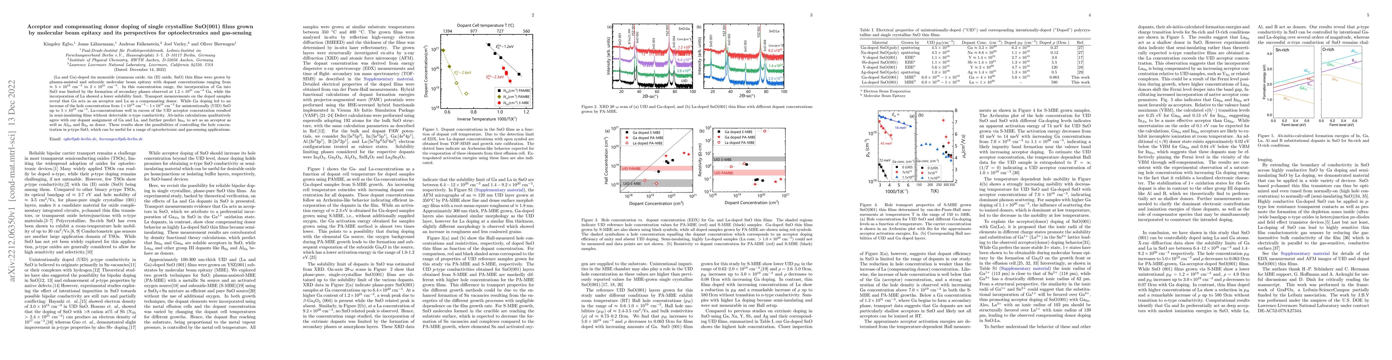
(La and Ga)-doped tin monoxide (stannous oxide, tin (II) oxide, SnO) thin films were grown by plasma-assisted and suboxide molecular beam epitaxy with dopant concentrations ranging from $\approx5\ti...

Thumbnail for Carrier Recombination in Highly Uniform and Phase-Pure GaAs/(Al,Ga)As
  Core/Shell Nanowire Arrays on Si(111): Mott Transition and Internal Quantum
  Efficiency

Carrier Recombination in Highly Uniform and Phase-Pure GaAs/(Al,Ga)As Core/Shell Nanowire Arrays on Si(111): Mott Transition and Internal Quantum Efficiency

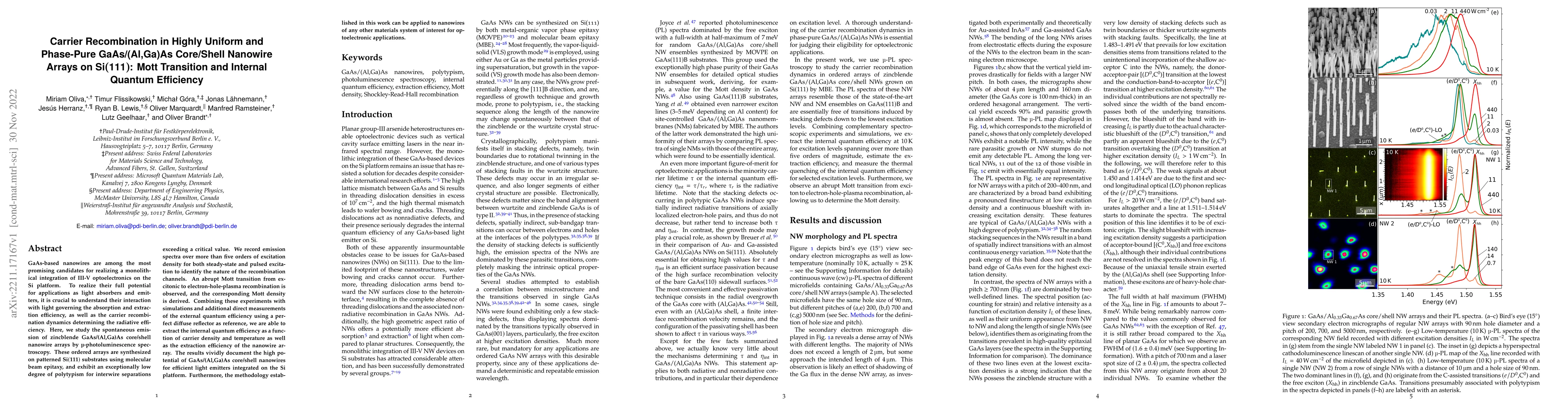
GaAs-based nanowires are among the most promising candidates for realizing a monolithical integration of III-V optoelectronics on the Si platform. To realize their full potential for applications as...

Thumbnail for Lattice parameters of
  Sc$_{\boldsymbol{\mathsf{x}}}$Al$_{\boldsymbol{\mathsf{1-x}}}$N layers grown
  on GaN(0001) by plasma-assisted molecular beam epitaxy

Lattice parameters of Sc$_{\boldsymbol{\mathsf{x}}}$Al$_{\boldsymbol{\mathsf{1-x}}}$N layers grown on GaN(0001) by plasma-assisted molecular beam epitaxy

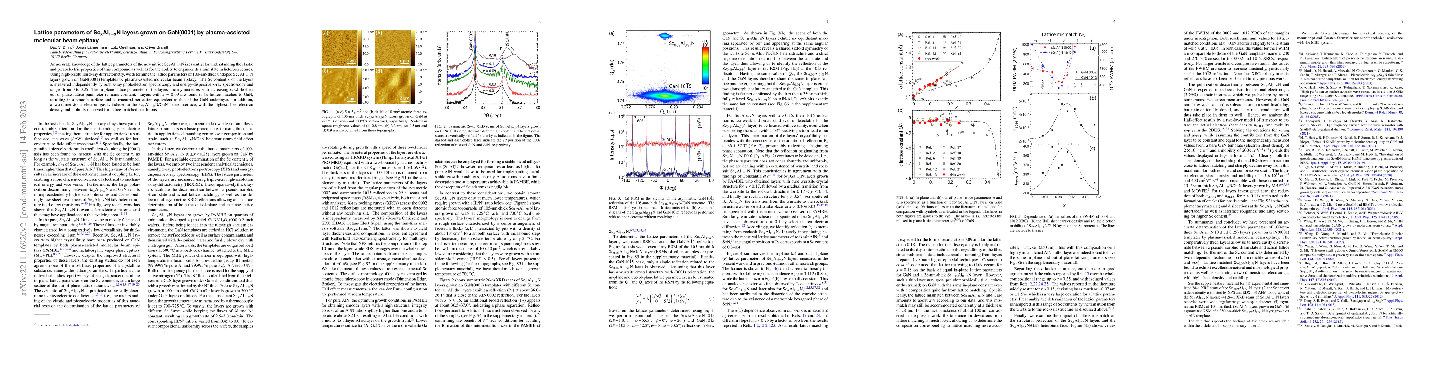
An accurate knowledge of the lattice parameters of the new nitride Sc$_\textit{x}$Al$_\textit{1-x}$N is essential for understanding the elastic and piezoelectric properties of this compound as well ...

Thumbnail for Epitaxial synthesis of unintentionally doped p-type SnO (001) via
  suboxide molecular beam epitaxy

Epitaxial synthesis of unintentionally doped p-type SnO (001) via suboxide molecular beam epitaxy

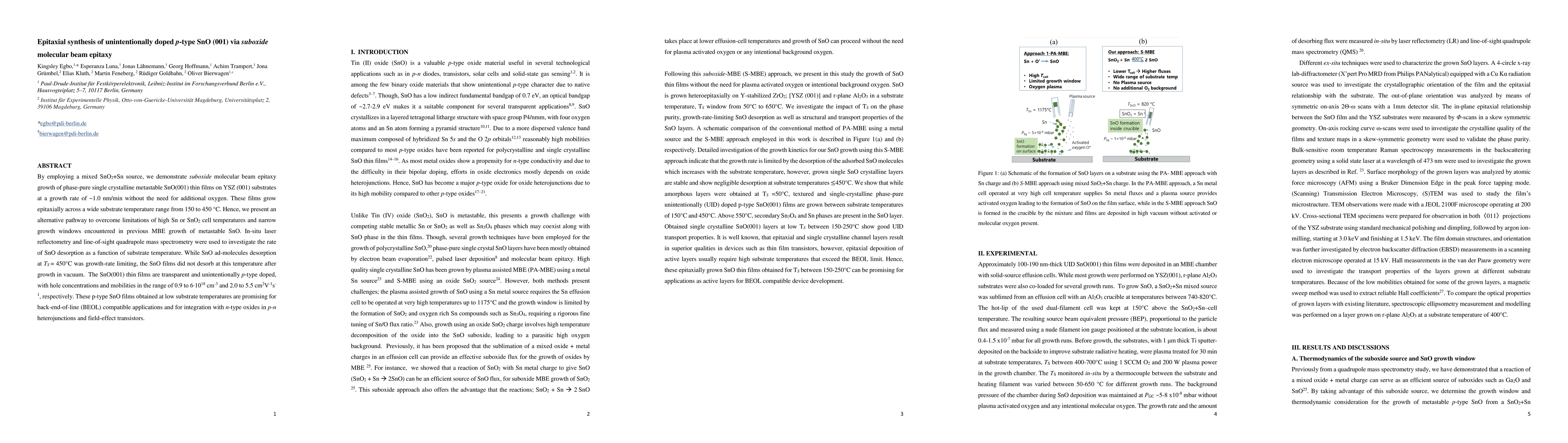
By employing a mixed SnO$_2$+Sn source, we demonstrate suboxide molecular beam epitaxy growth of phase-pure single crystalline metastable SnO(001) thin films at a growth rate of ~1.0nm/min without t...

Thumbnail for Interface recombination in Ga- and N-polar GaN/(Al,Ga)N quantum wells
  grown by molecular beam epitaxy

Interface recombination in Ga- and N-polar GaN/(Al,Ga)N quantum wells grown by molecular beam epitaxy

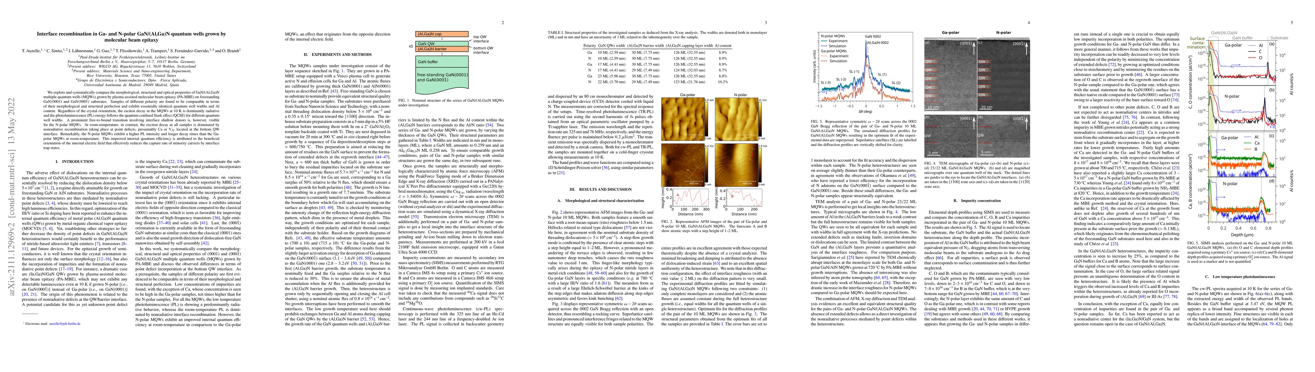
We explore and systematically compare the morphological, structural and optical properties of GaN/(Al,Ga)N multiple quantum wells (MQWs) grown by plasma-assisted molecular beam epitaxy (PA-MBE) on f...

Thumbnail for Dislocation and Indium Droplet Related Emission Inhomogeneities in InGaN
  LEDs

Dislocation and Indium Droplet Related Emission Inhomogeneities in InGaN LEDs

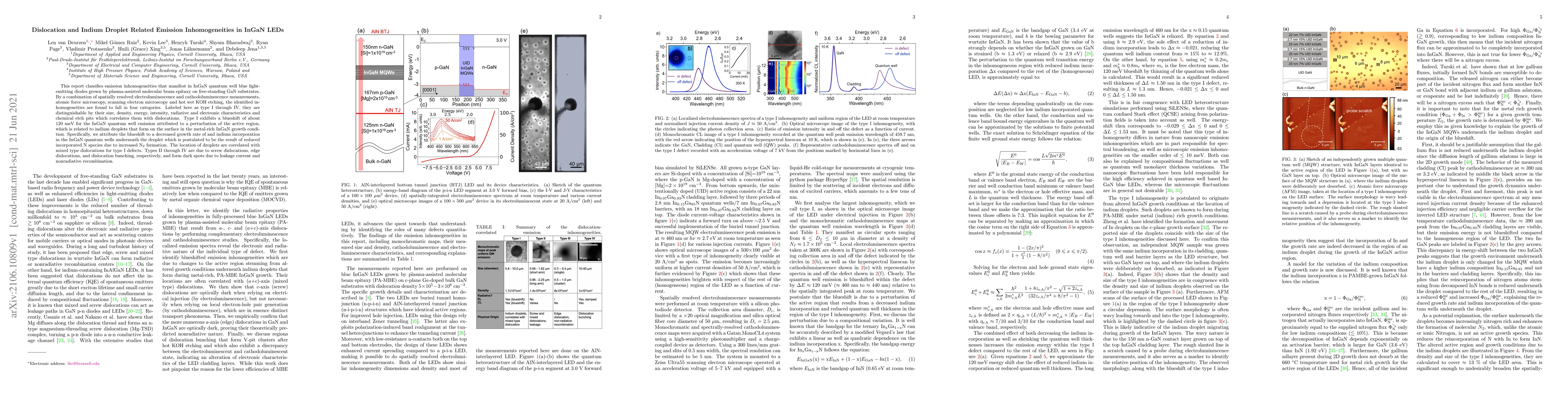
This report classifies emission inhomogeneities that manifest in InGaN quantum well blue light-emitting diodes grown by plasma-assisted molecular beam epitaxy on free-standing GaN substrates. By a c...

Thumbnail for Molecular beam epitaxy of single-crystalline bixbyite
  (In$_{1-x}$Ga$_x$)$_2$O$_3$ films ($x \leq 0.18$): Structural properties and
  consequences of compositional inhomogeneity

Molecular beam epitaxy of single-crystalline bixbyite (In$_{1-x}$Ga$_x$)$_2$O$_3$ films ($x \leq 0.18$): Structural properties and consequences of compositional inhomogeneity

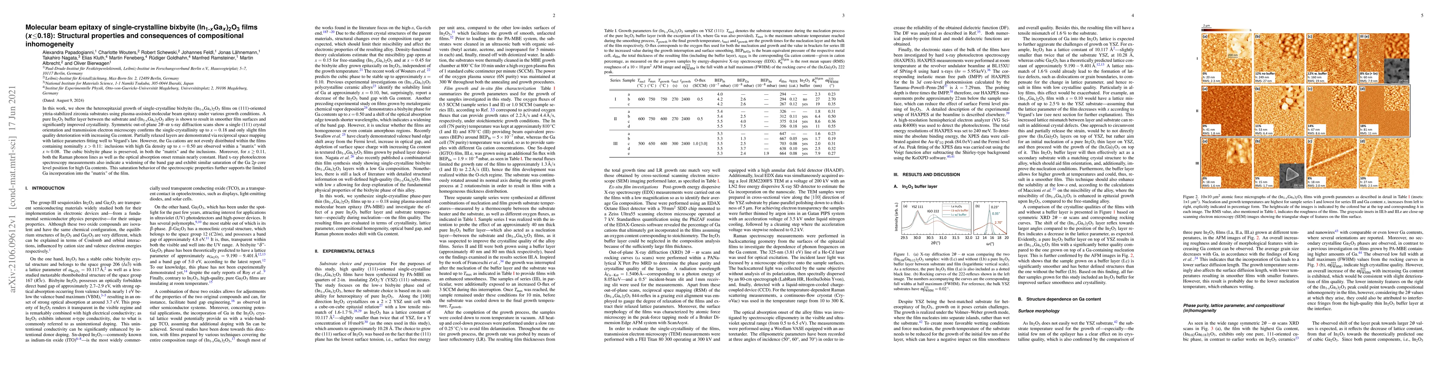
In this work, we show the heteroepitaxial growth of single-crystalline bixbyite (In$_{1-x}$Ga$_x$)$_2$O$_3$ films on (111)-oriented yttria-stabilized zirconia substrates using plasma-assisted molecu...

Thumbnail for Carrier diffusion in GaN -- a cathodoluminescence study. III: Nature of
  nonradiative recombination at threading dislocations

Carrier diffusion in GaN -- a cathodoluminescence study. III: Nature of nonradiative recombination at threading dislocations

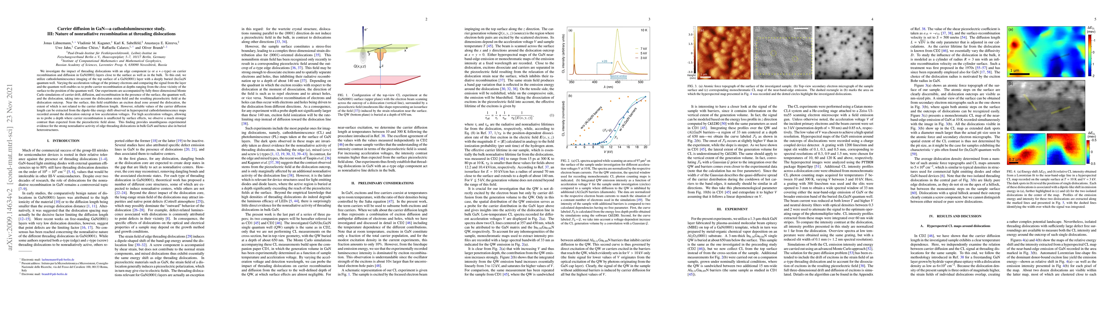
We investigate the impact of threading dislocations with an edge component (a or a+c-type) on carrier recombination and diffusion in GaN(0001) layers close to the surface as well as in the bulk. To ...

Thumbnail for Carrier diffusion in GaN -- a cathodoluminescence study. II: Ambipolar
  vs. exciton diffusion

Carrier diffusion in GaN -- a cathodoluminescence study. II: Ambipolar vs. exciton diffusion

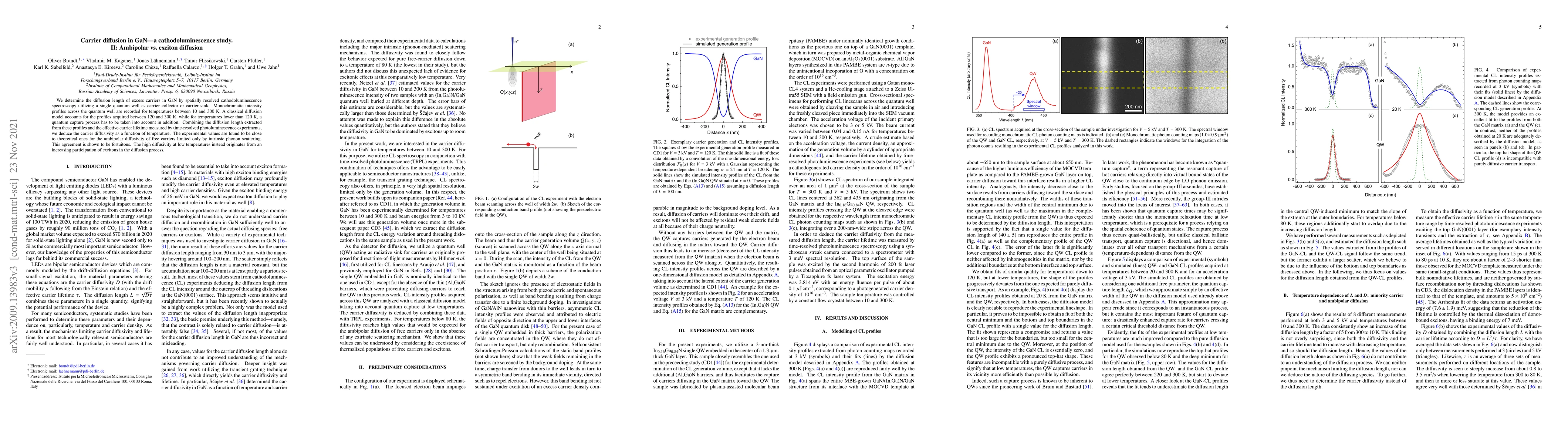
We determine the diffusion length of excess carriers in GaN by spatially resolved cathodoluminescence spectroscopy utilizing a single quantum well as carrier collector or carrier sink. Monochromatic...

Thumbnail for Beam damage of single semiconductor nanowires during X-ray nano beam
  diffraction experiments

Beam damage of single semiconductor nanowires during X-ray nano beam diffraction experiments

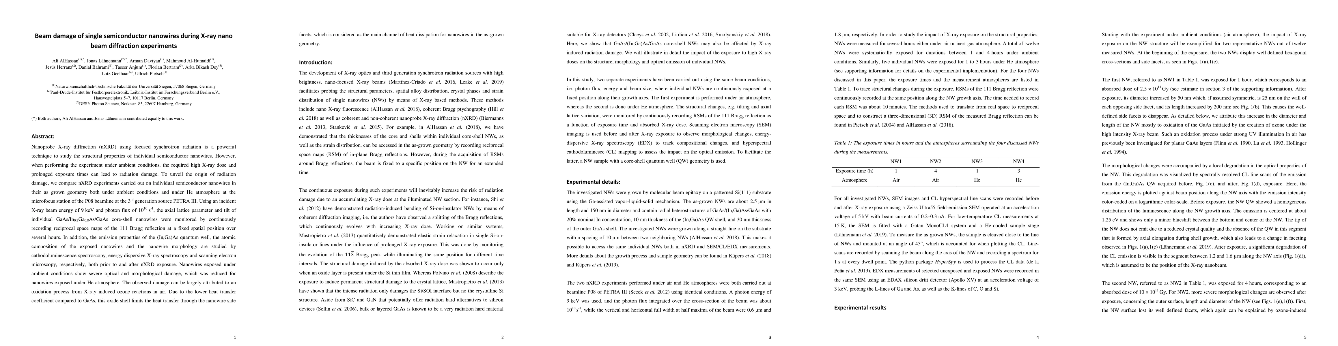
Nanoprobe X-ray diffraction (nXRD) using focused synchrotron radiation is a powerful technique to study the structural properties of individual semiconductor nanowires. However, when performing the ...

Thumbnail for Carrier diffusion in GaN -- a cathodoluminescence study. I:
  Temperature-dependent generation volume

Carrier diffusion in GaN -- a cathodoluminescence study. I: Temperature-dependent generation volume

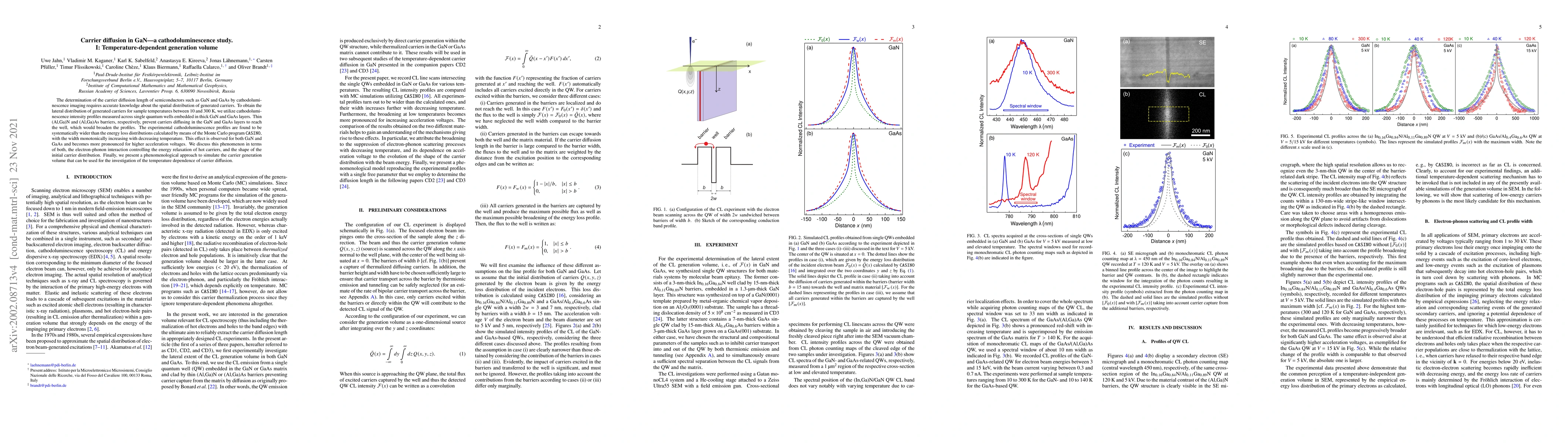
The determination of the carrier diffusion length of semiconductors such as GaN and GaAs by cathodoluminescence imaging requires accurate knowledge about the spatial distribution of generated carrie...

Thumbnail for Spatially-resolved luminescence and crystal structure of single
  core-shell nanowires measured in the as-grown geometry

Spatially-resolved luminescence and crystal structure of single core-shell nanowires measured in the as-grown geometry

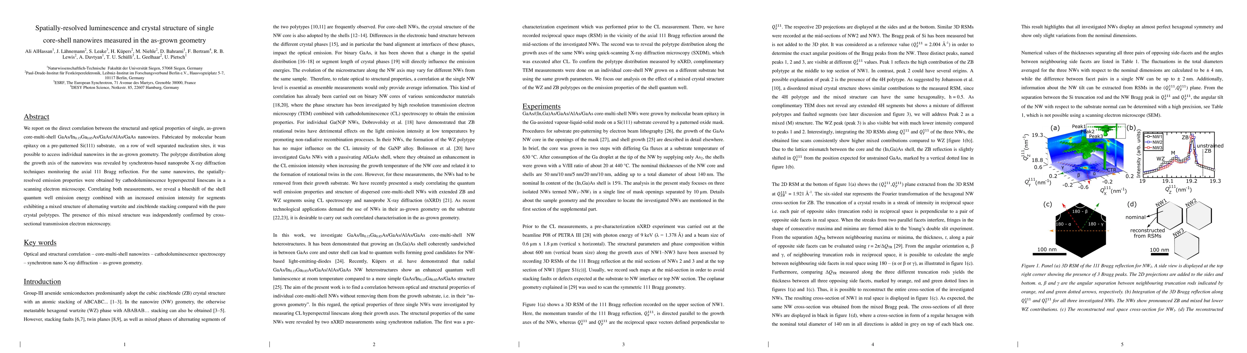
We report on the direct correlation between the structural and optical properties of single, as-grown core-multi-shell GaAs/In$_{0.15}$Ga$_{0.85}$As/GaAs/AlAs/GaAs nanowires. Fabricated by molecular...

Thumbnail for Correlated and in-situ electrical transmission electron microscopy
  studies and related membrane fabrication

Correlated and in-situ electrical transmission electron microscopy studies and related membrane fabrication

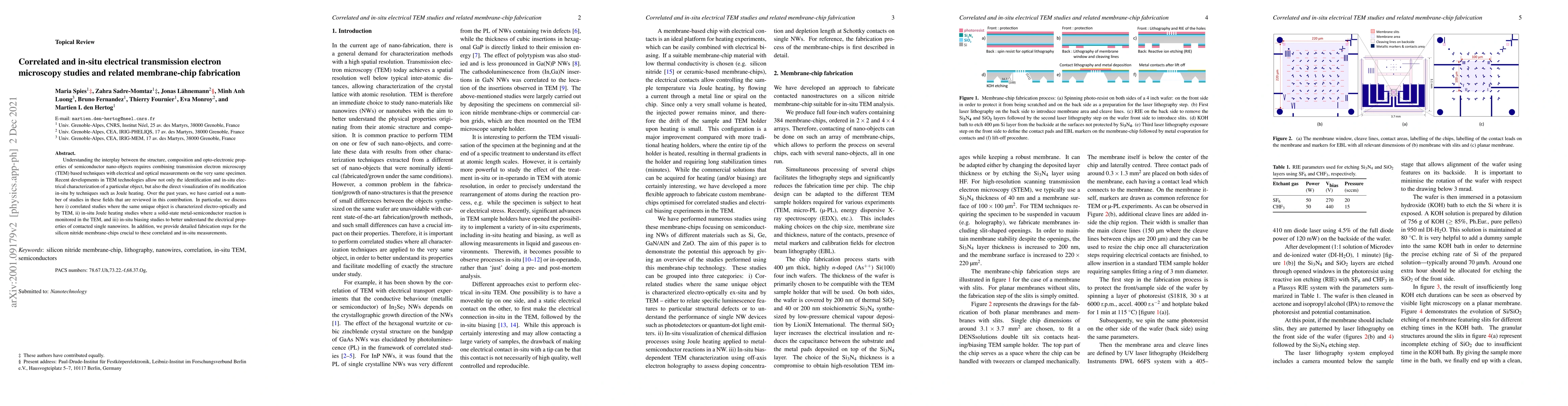
Understanding the interplay between the structure, composition and opto-electronic properties of semiconductor nano-objects requires combining transmission electron microscopy (TEM) based techniques...

Thumbnail for Plasma-assisted molecular beam epitaxy of NiO on GaN(00.1)

Plasma-assisted molecular beam epitaxy of NiO on GaN(00.1)

The growth of NiO on GaN(00.1) substrates by plasma-assisted molecular beam epitaxy under oxygen rich conditions was investigated at growth temperatures between 100 $^{\circ}$C and 850 $^{\circ}$C. ...

Thumbnail for Self-assembly of well-separated AlN nanowires directly on sputtered
  metallic TiN films

Self-assembly of well-separated AlN nanowires directly on sputtered metallic TiN films

We demonstrate the self-assembled formation of AlN nanowires by molecular beam epitaxy on sputtered TiN films on sapphire. This choice of substrate allows growth at an exceptionally high temperature...

Thumbnail for Electroluminescence and current-voltage measurements of single
  (In,Ga)N/GaN nanowire light-emitting diodes in the nanowire ensemble

Electroluminescence and current-voltage measurements of single (In,Ga)N/GaN nanowire light-emitting diodes in the nanowire ensemble

We present the combined analysis of the electroluminescence (EL) as well as the current-voltage (I-V) behavior of single, freestanding (In,Ga)N/GaN nanowire (NW) light-emitting diodes (LEDs) in an u...

Thumbnail for Kinetics, thermodynamics, and catalysis of the cation incorporation into
  GeO$_2$, SnO$_2$, and (Sn$_x$Ge$_{1-x}$)O$_2$ during suboxide molecular beam
  epitaxy

Kinetics, thermodynamics, and catalysis of the cation incorporation into GeO$_2$, SnO$_2$, and (Sn$_x$Ge$_{1-x}$)O$_2$ during suboxide molecular beam epitaxy

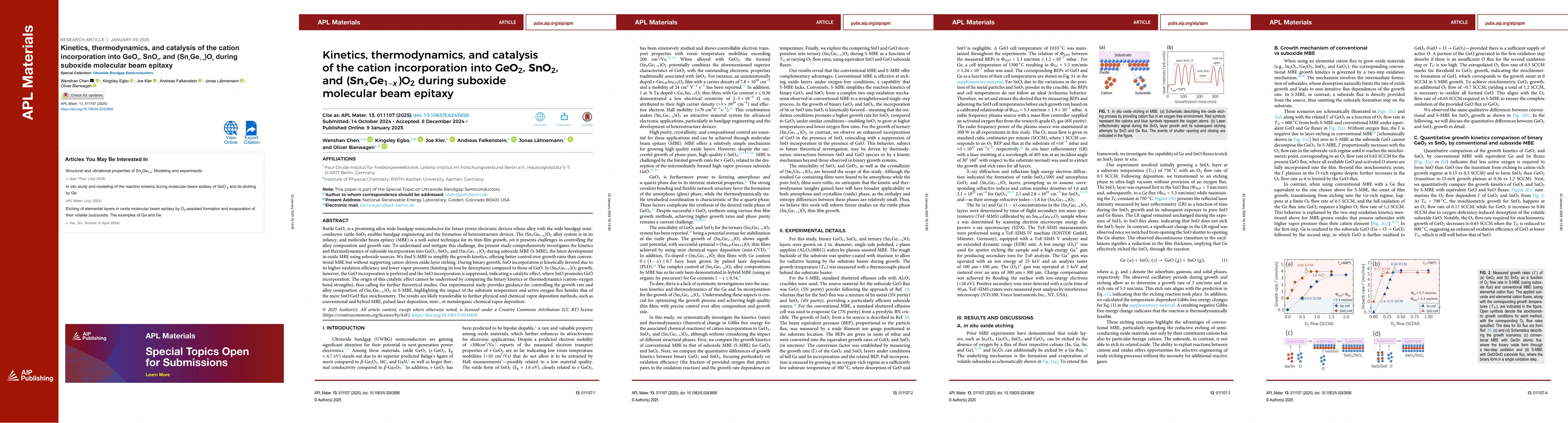
Rutile GeO$_2$ is a promising ultra-wide bandgap semiconductor for future power electronic devices whose alloy with the wide bandgap semiconductor rutile-SnO$_2$ enables bandgap engineering and the fo...

Thumbnail for Growth of compositionally uniform
  $\mathrm{In}_{x}\mathrm{Ga}_{1-x}\mathrm{N}$ layers with low relaxation
  degree on GaN by molecular beam epitaxy

Growth of compositionally uniform $\mathrm{In}_{x}\mathrm{Ga}_{1-x}\mathrm{N}$ layers with low relaxation degree on GaN by molecular beam epitaxy

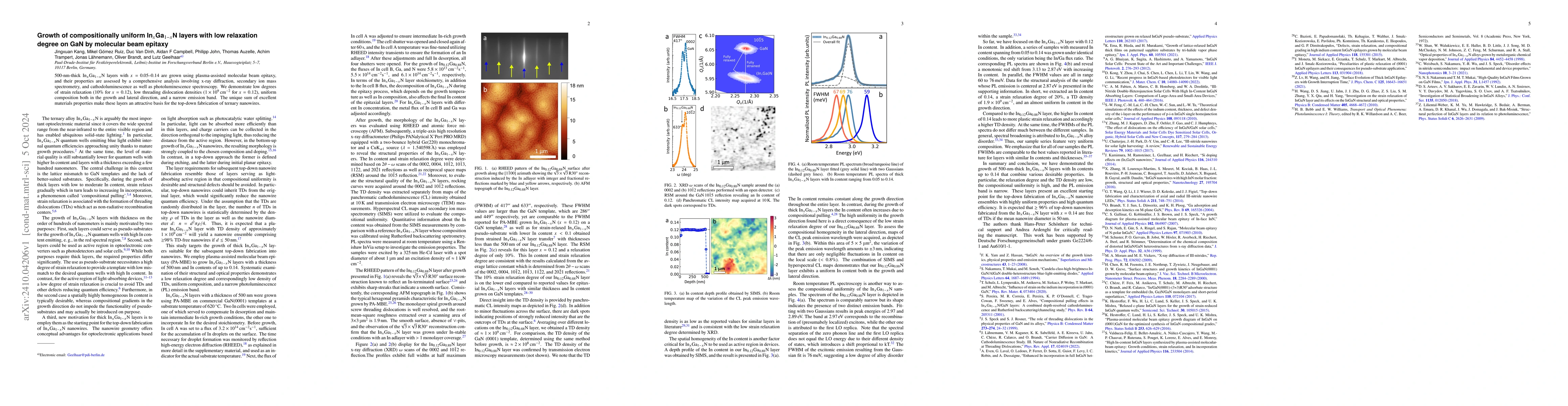
500-nm-thick $\mathrm{In}_{x}\mathrm{Ga}_{1-x}\mathrm{N}$ layers with $x=$ 0.05-0.14 are grown using plasma-assisted molecular beam epitaxy, and their properties are assessed by a comprehensive analys...

Thumbnail for Dislocation correlations in GaN epitaxial films revealed by EBSD and XRD

Dislocation correlations in GaN epitaxial films revealed by EBSD and XRD

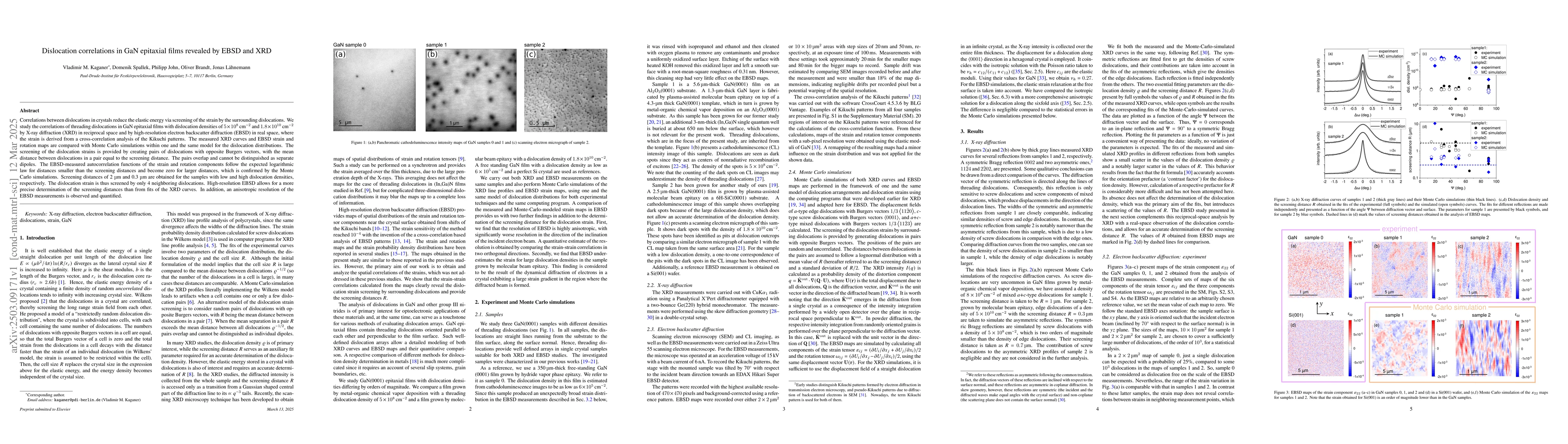
Correlations between dislocations in crystals reduce the elastic energy via screening of the strain by the surrounding dislocations. We study the correlations of threading dislocations in GaN epitaxia...

Thumbnail for Molecular Beam Epitaxy of Al$\mathrm{_{1-x}}$Sc$\mathrm{_{x}}$N Nanowires: Towards Group-III Nitride Piezoelectric Nanogenerators with Enhanced Response

Molecular Beam Epitaxy of Al$\mathrm{_{1-x}}$Sc$\mathrm{_{x}}$N Nanowires: Towards Group-III Nitride Piezoelectric Nanogenerators with Enhanced Response

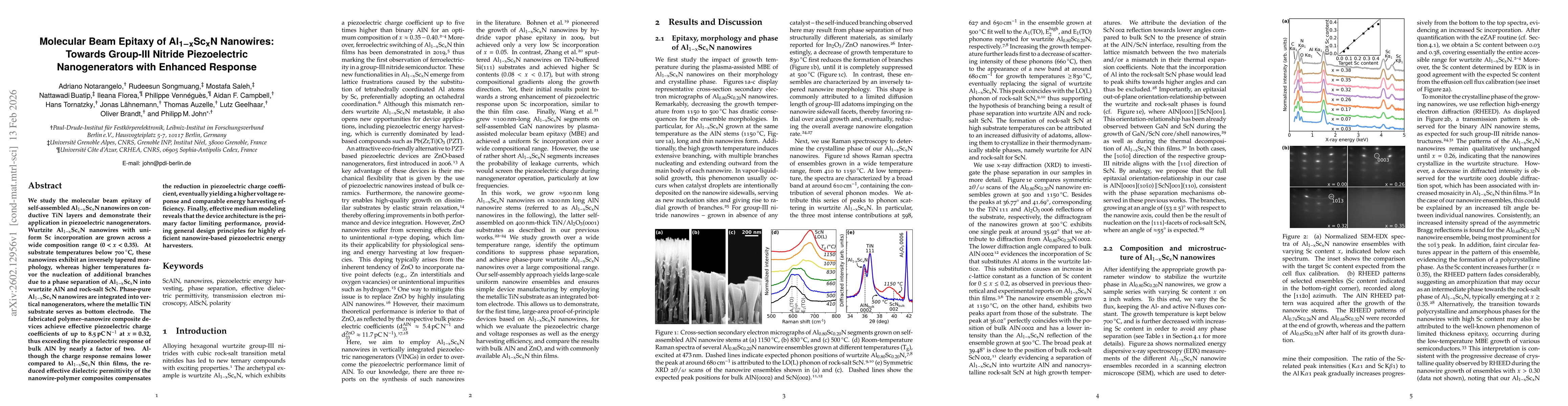
We study the molecular beam epitaxy of self-assembled Al$\mathrm{_{1-x}}$Sc$\mathrm{_{x}}$N nanowires on conductive TiN layers and demonstrate their application in piezoelectric nanogenerators. Wurtzi...

This website uses cookies to ensure you get the best experience. Learn more