Academic Profile
Statistics
Similar Authors
Papers on arXiv
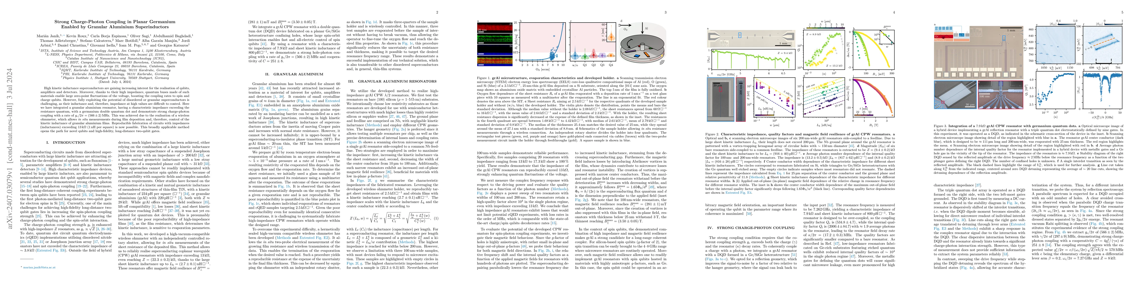
High kinetic inductance superconductors are gaining increasing interest for the realisation of qubits, amplifiers and detectors. Moreover, thanks to their high impedance, quantum buses made of such ...
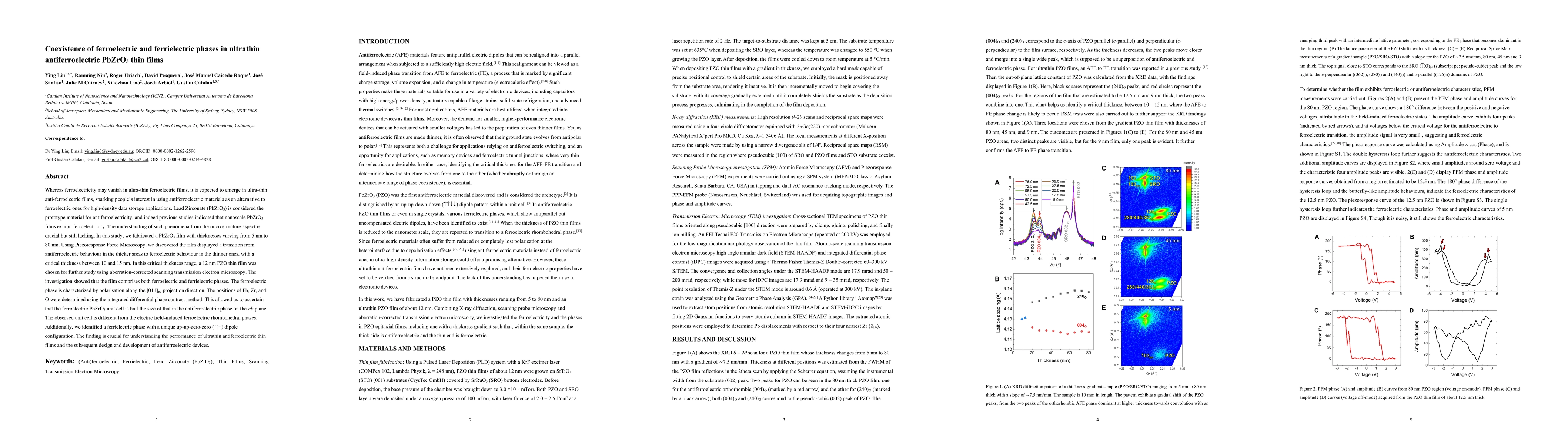
Whereas ferroelectricity may vanish in ultra-thin ferroelectric films, it is expected to emerge in ultra-thin anti-ferroelectric films, sparking people's interest in using antiferroelectric material...
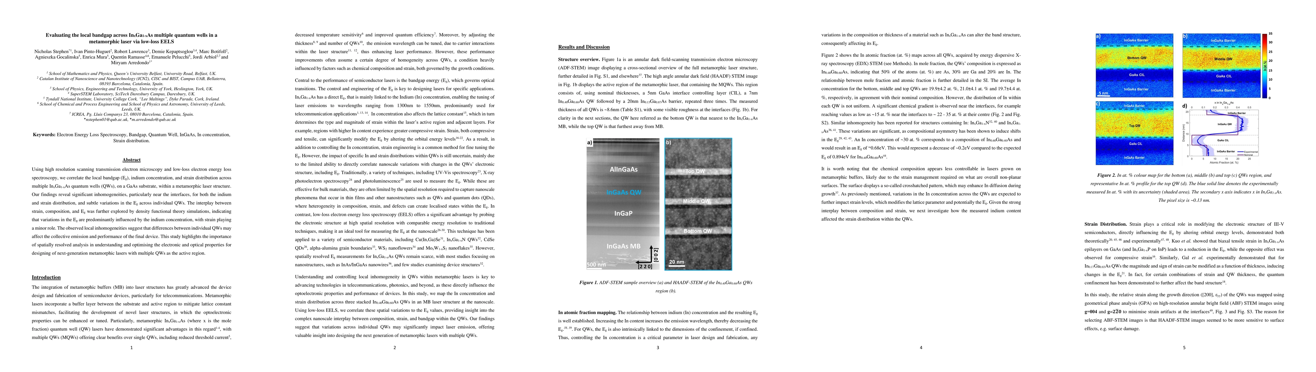
We investigate spatially resolved variations in the bandgap energy across multiple InxGa1-xAs quantum wells (QWs) on a GaAs substrate within a metamorphic laser structure. Using high resolution scan...
New approaches such as selective area growth, where crystal growth is lithographically controlled, allow the integration of bottom-up grown semiconductor nanomaterials in large-scale classical and q...
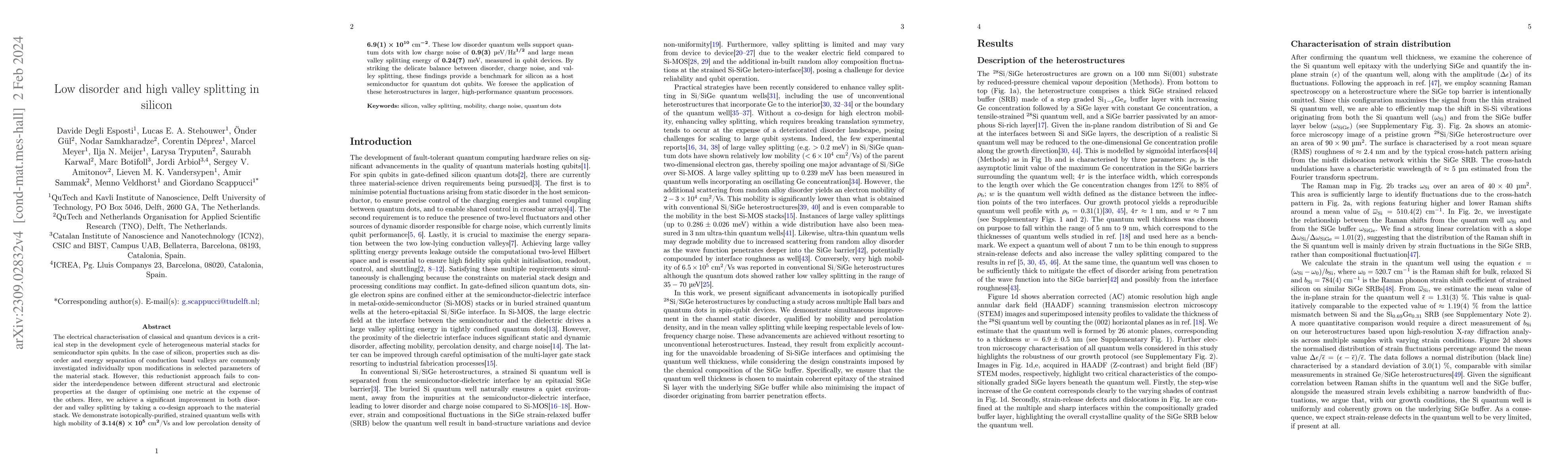
The electrical characterisation of classical and quantum devices is a critical step in the development cycle of heterogeneous material stacks for semiconductor spin qubits. In the case of silicon, p...
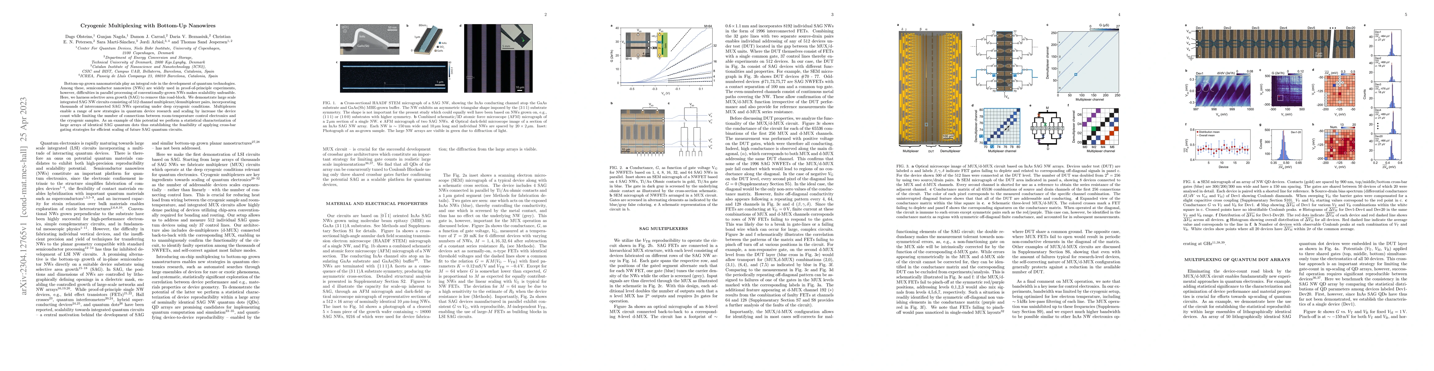
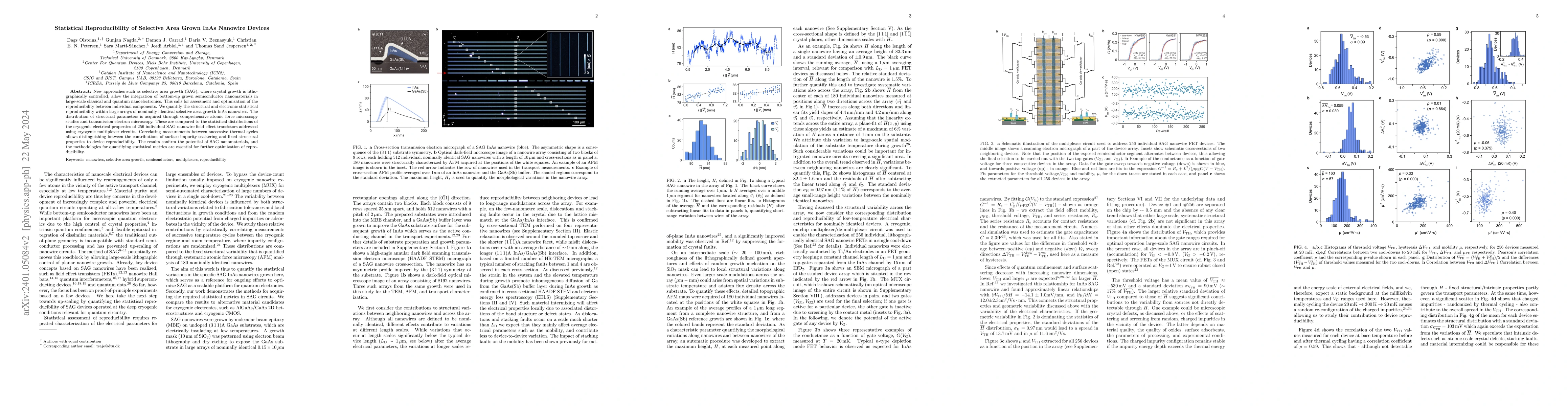
Bottom-up grown nanomaterials play an integral role in the development of quantum technologies. Among these, semiconductor nanowires (NWs) are widely used in proof-of-principle experiments, however,...
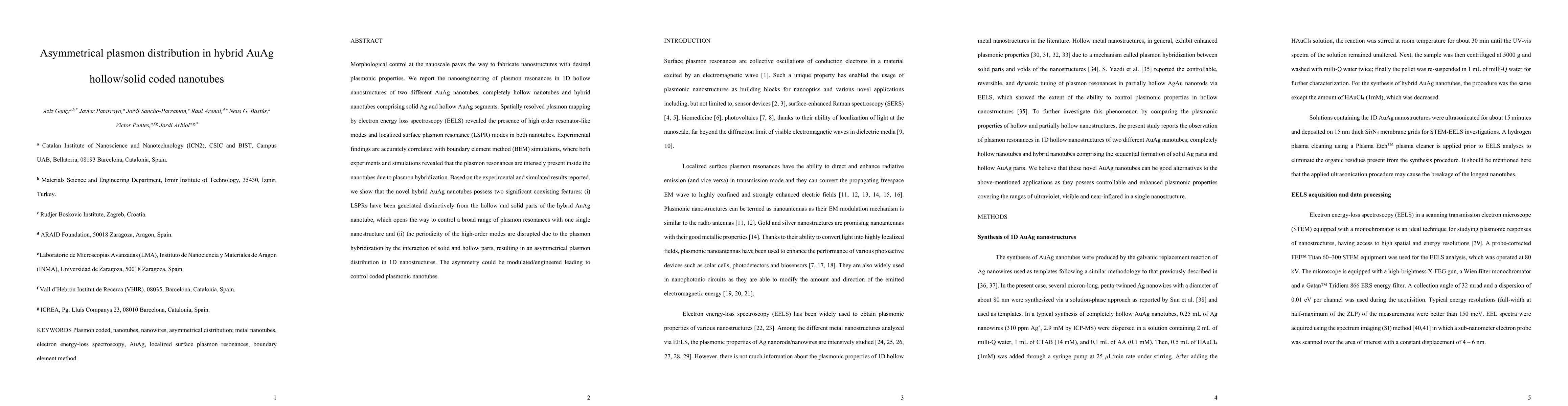
Morphological control at the nanoscale paves the way to fabricate nanostructures with desired plasmonic properties. We report the nanoengineering of plasmon resonances in 1D hollow nanostructures of...
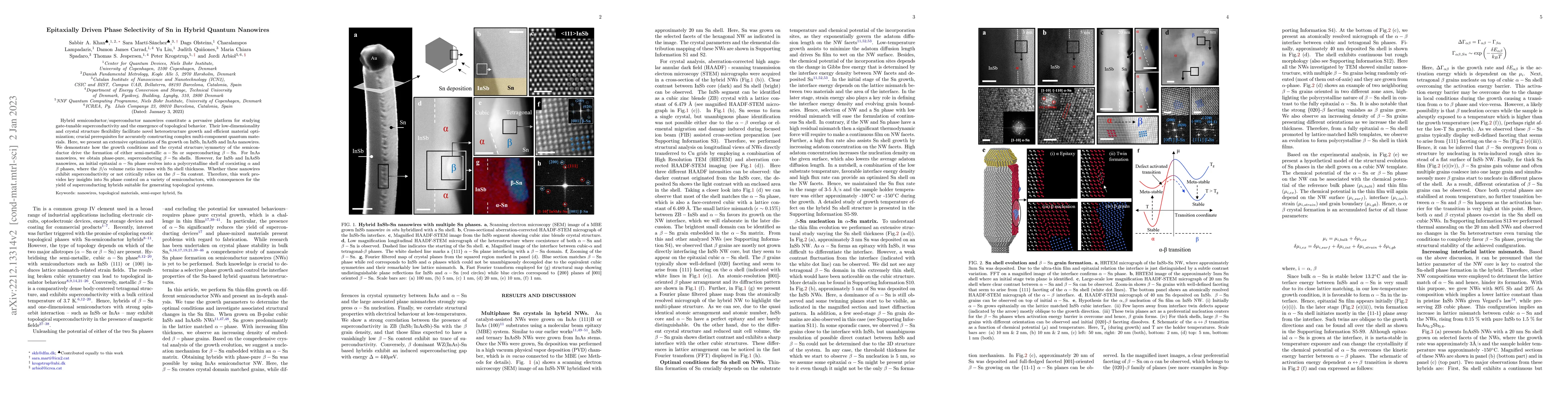
Hybrid semiconductor/superconductor nanowires constitute a pervasive platform for studying gate-tunable superconductivity and the emergence of topological behavior. Their low-dimensionality and crys...
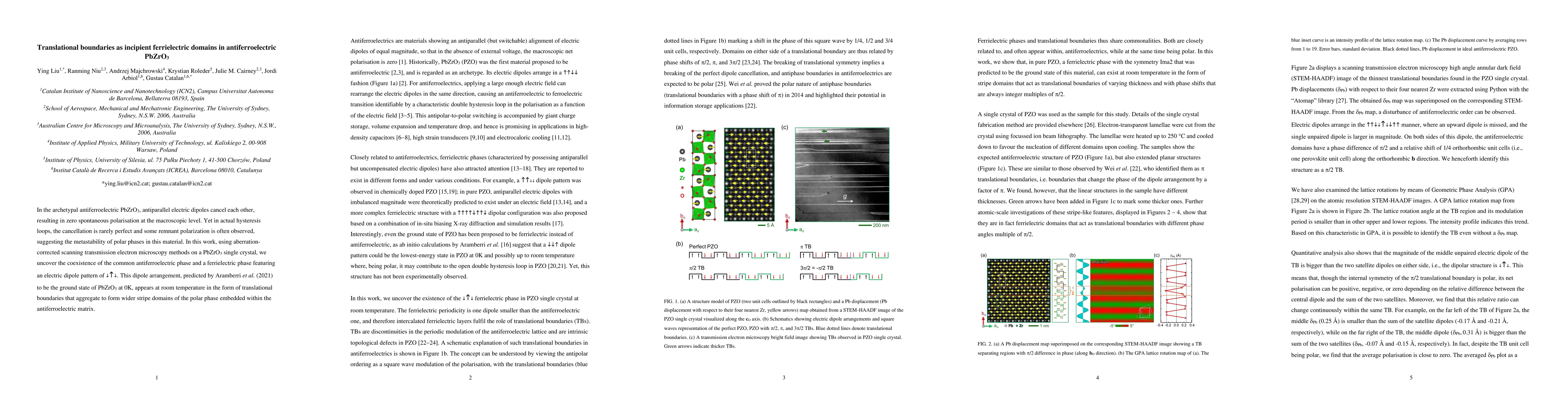
In the archetypal antiferroelectric PbZrO3, antiparallel electric dipoles cancel each other, resulting in zero spontaneous polarisation at the macroscopic level. Yet in actual hysteresis loops, the ...
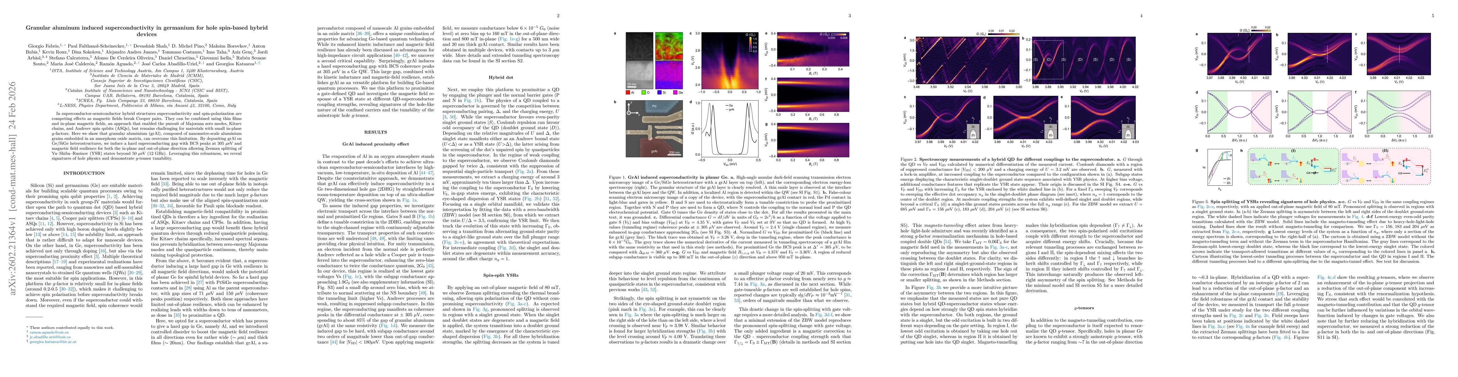
The co-integration of spin, superconducting, and topological systems is emerging as an exciting pathway for scalable and high-fidelity quantum information technology. High-mobility planar germanium ...
Hybrid semiconductor-superconductor devices hold great promise for realizing topological quantum computing with Majorana zero modes (MZMs). However, multiple claims of Majorana detection, based on e...
Selective area growth (SAG) of nanowires and networks promise a route toward scalable electronics, photonics and quantum devices based on III-V semiconductor materials. The potential of high-mobilit...
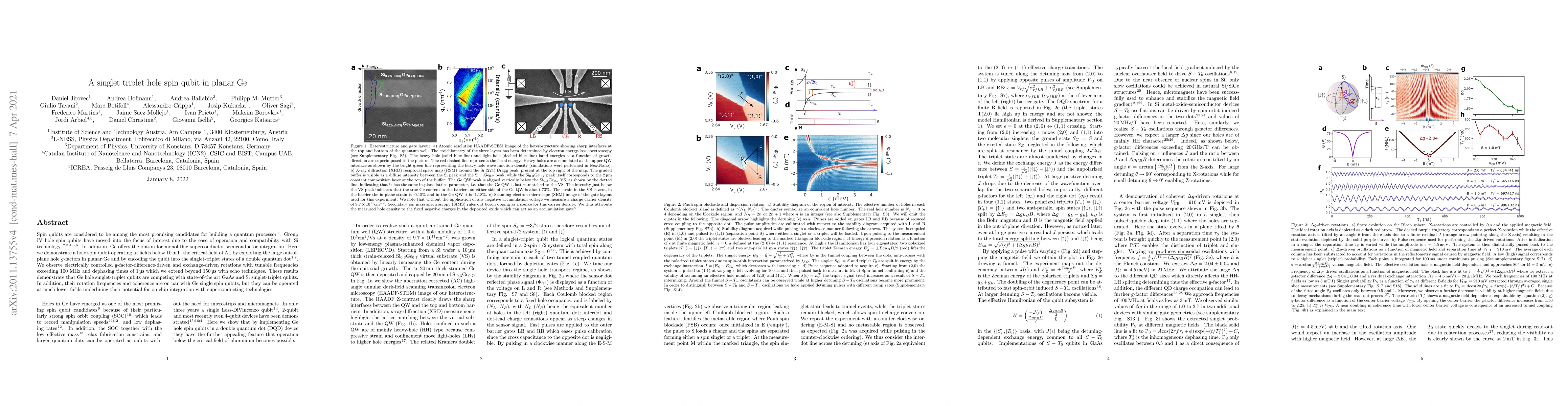
Spin qubits are considered to be among the most promising candidates for building a quantum processor. GroupIV hole spin qubits have moved into the focus of interest due to the ease of operation and...
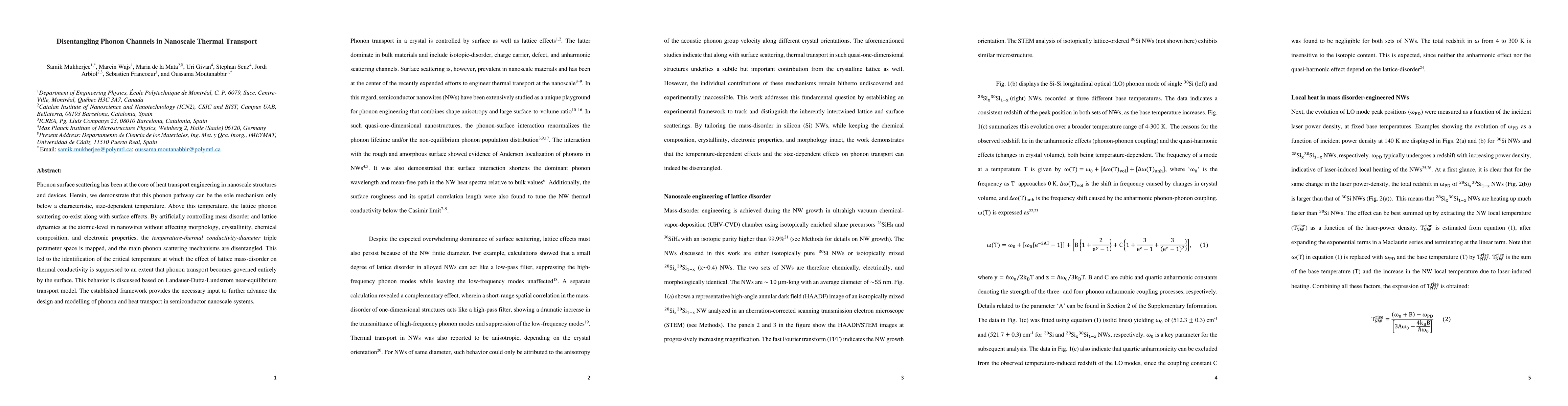
Phonon surface scattering has been at the core of heat transport engineering in nanoscale structures and devices. Herein, we demonstrate that this phonon pathway can be the sole mechanism only below...
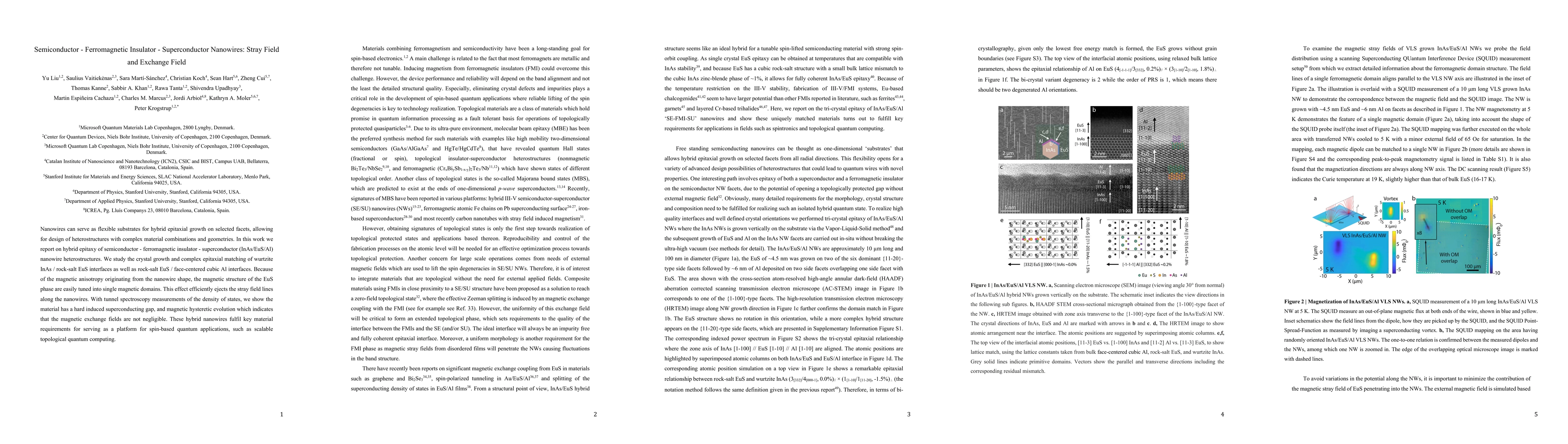
Nanowires can serve as flexible substrates for hybrid epitaxial growth on selected facets, allowing for design of heterostructures with complex material combinations and geometries. In this work we ...
Hybrid semiconductor-ferromagnetic insulator heterostructures are interesting due to their tunable electronic transport, self-sustained stray field and local proximitized magnetic exchange. In this ...
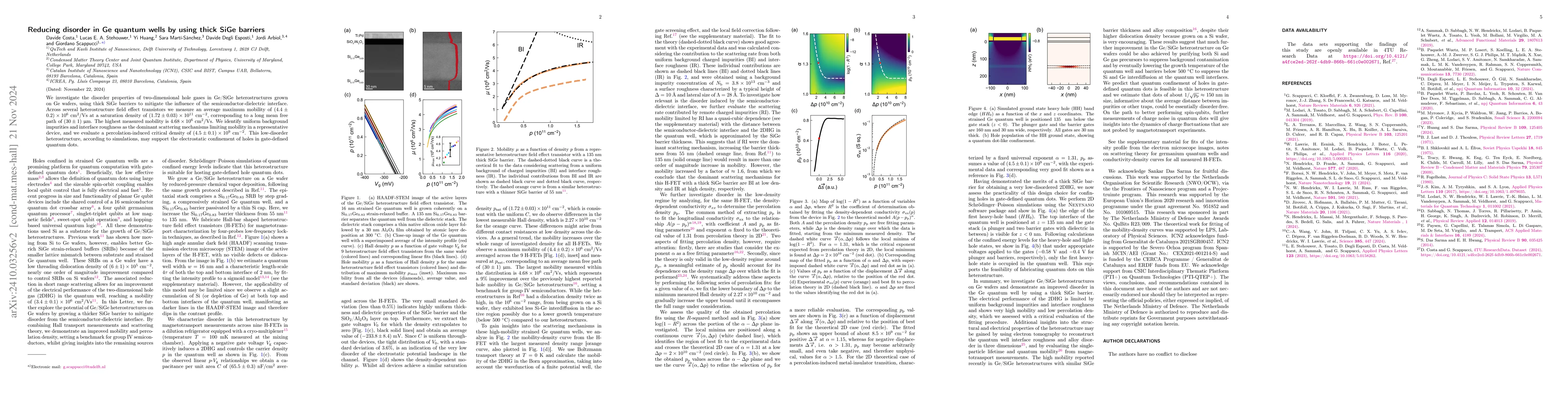
We investigate the disorder properties of two-dimensional hole gases in Ge/SiGe heterostructures grown on Ge wafers, using thick SiGe barriers to mitigate the influence of the semiconductor-dielectric...
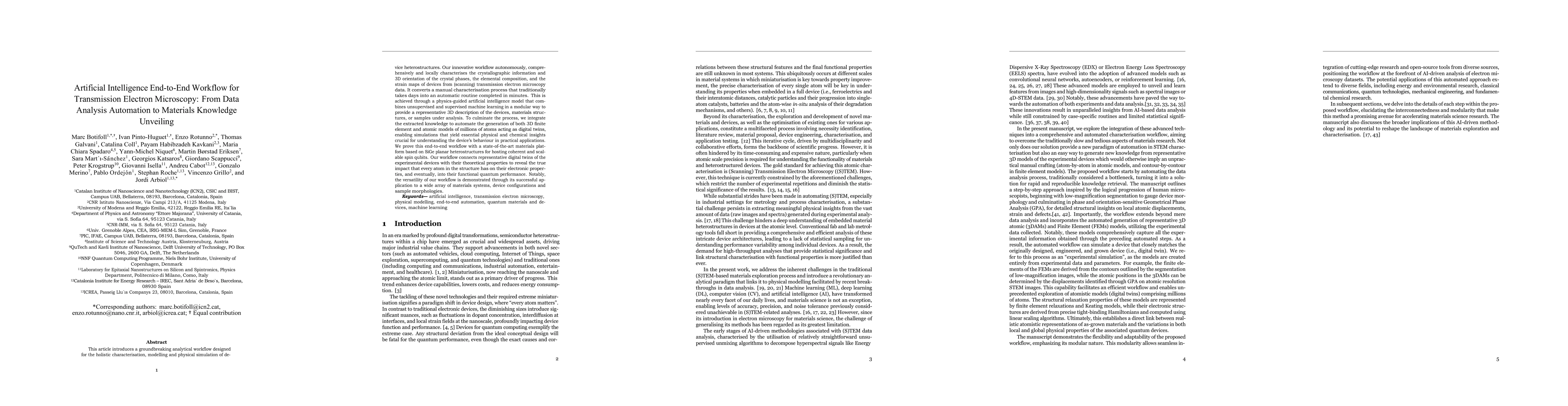
This article introduces a groundbreaking analytical workflow designed for the holistic characterisation, modelling and physical simulation of device heterostructures. Our innovative workflow autonomou...
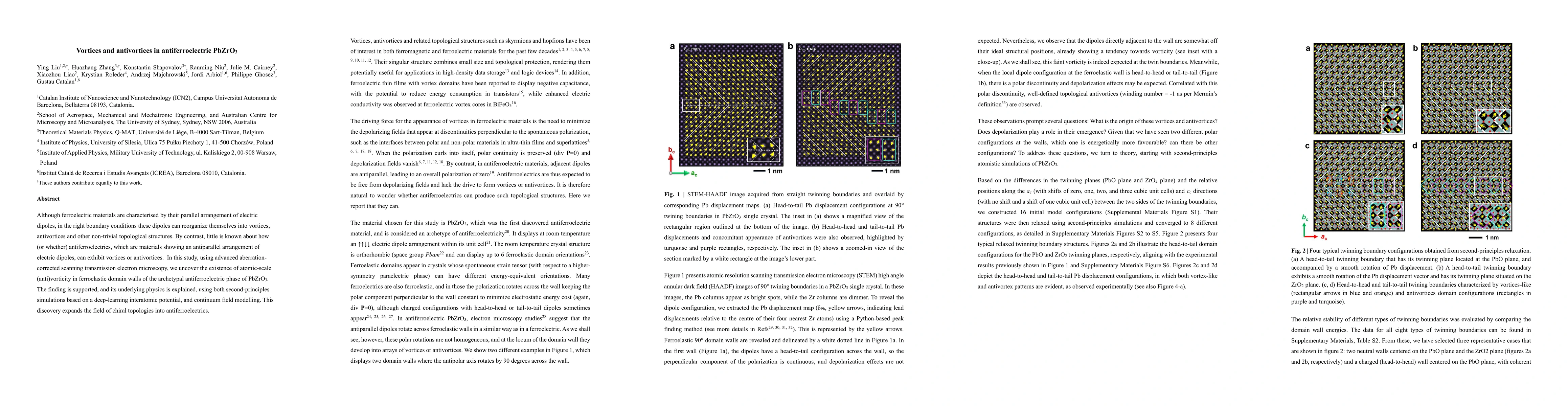
Although ferroelectric materials are characterised by their parallel arrangement of electric dipoles, in the right boundary conditions these dipoles can reorganize themselves into vortices, antivortic...
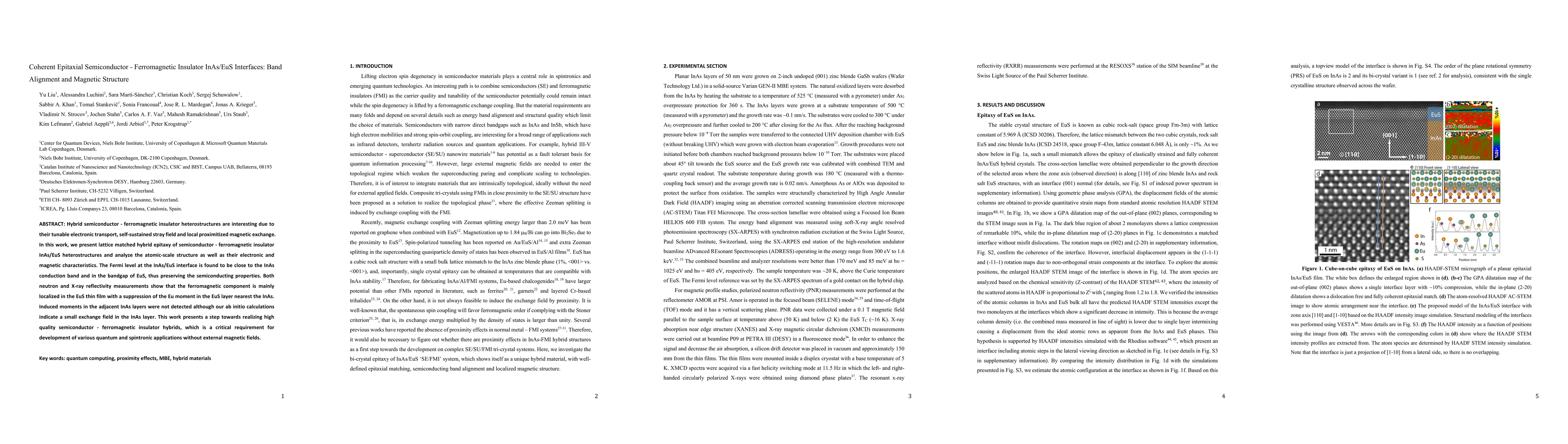
Atomic resolution electron microscopy, particularly high-angle annular dark-field scanning transmission electron microscopy, has become an essential tool for many scientific fields, when direct visual...
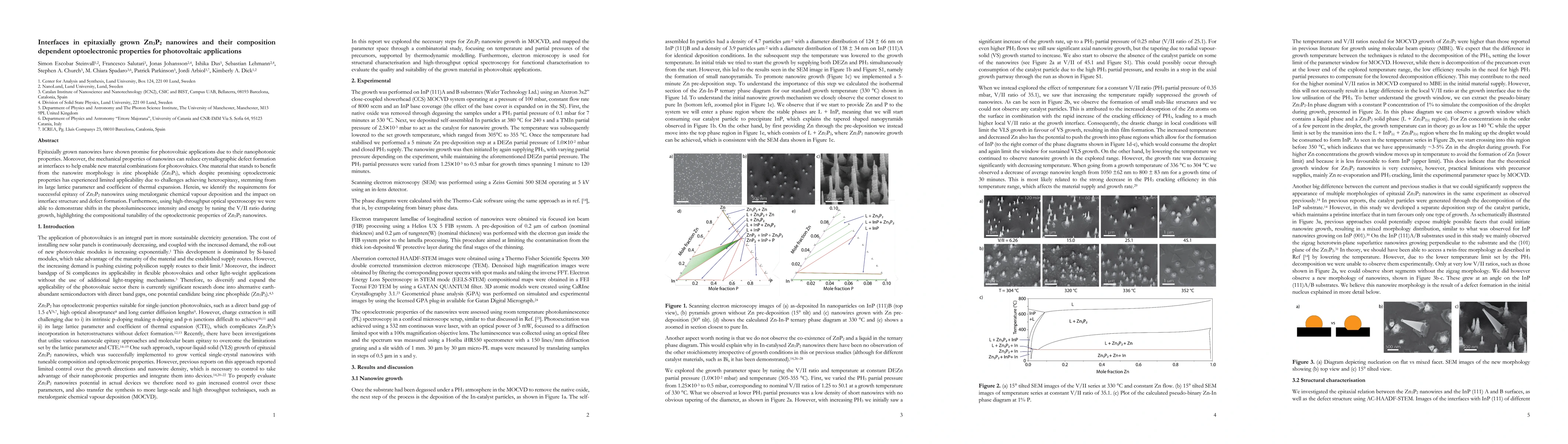
Epitaxially grown nanowires have shown promise for photovoltaic applications due to their nanophotonic properties. Moreover, the mechanical properties of nanowires can reduce crystallographic defect f...
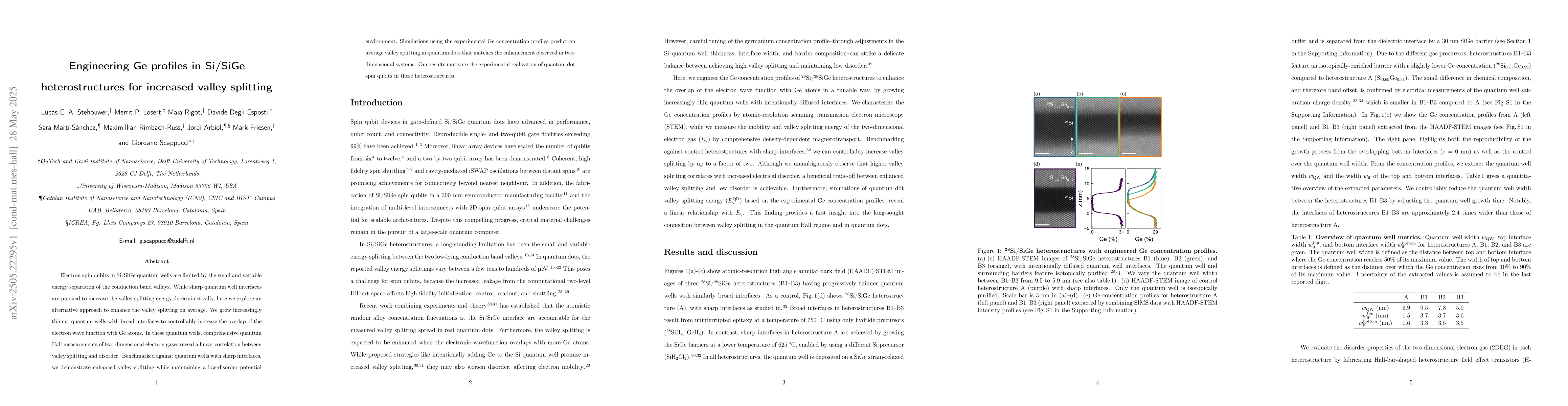
Electron spin qubits in Si/SiGe quantum wells are limited by the small and variable energy separation of the conduction band valleys. While sharp quantum well interfaces are pursued to increase the va...
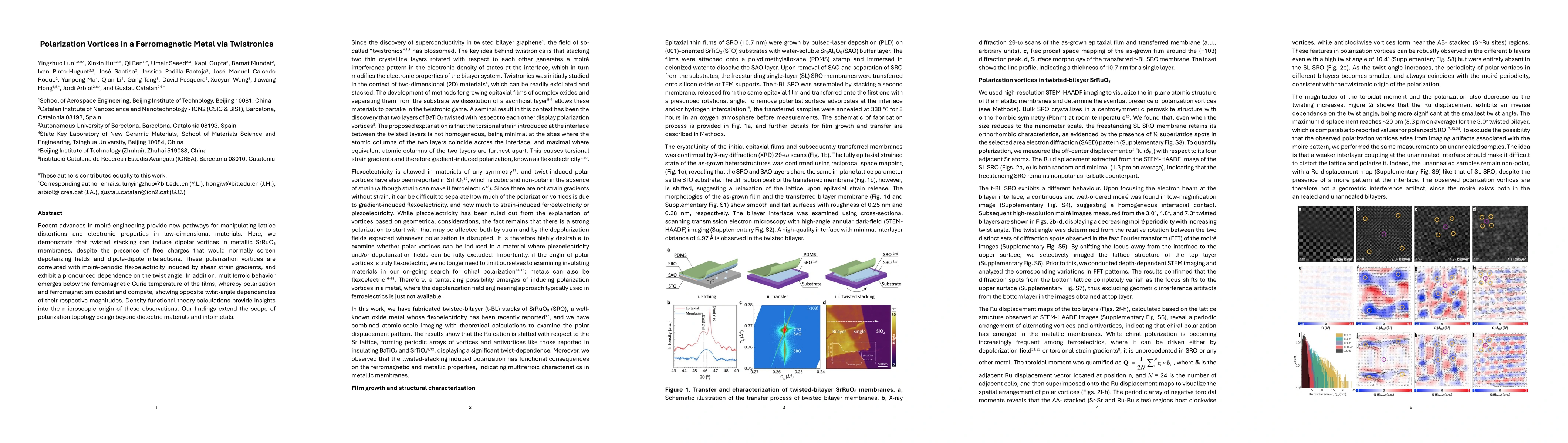
Recent advances in moire engineering provide new pathways for manipulating lattice distortions and electronic properties in low-dimensional materials. Here, we demonstrate that twisted stacking can in...
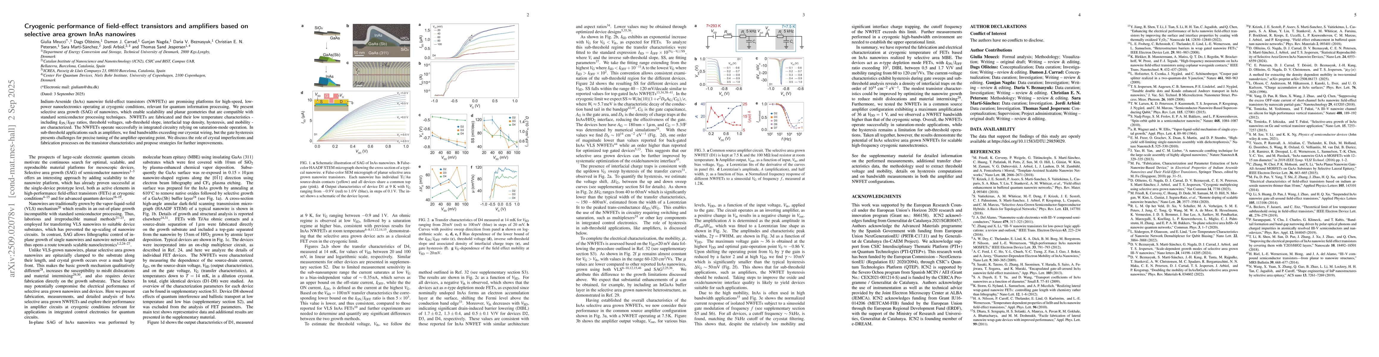
Indium-Arsenide (InAs) nanowire field-effect transistors (NWFETs) are promising platforms for high-speed, low power nanoelectronics operating at cryogenic conditions, relevant for quantum information ...
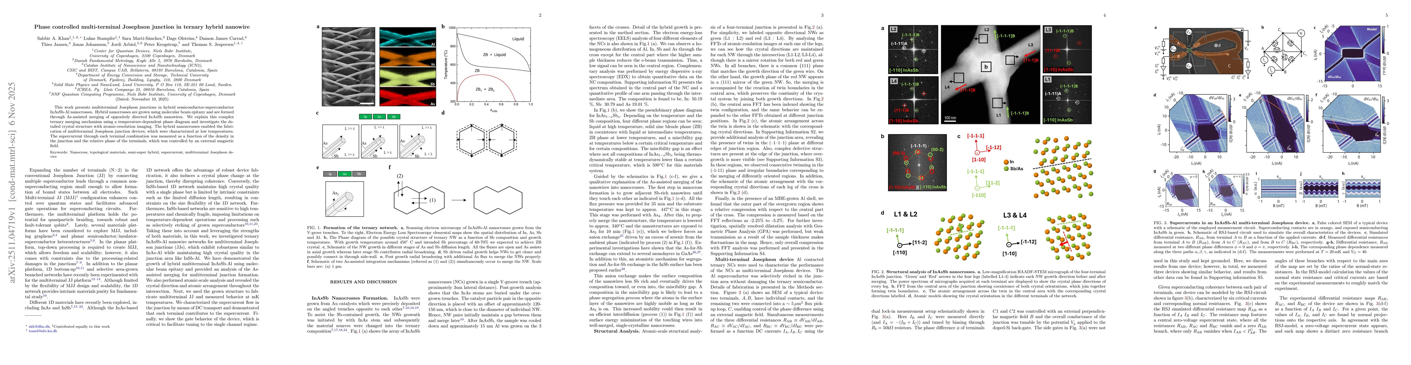
This work presents multiterminal Josephson junctions in hybrid semiconductor-superconductor InAsSb-Al nanocrosses. Hybrid nanocrosses are grown using molecular beam epitaxy and are formed through As-a...
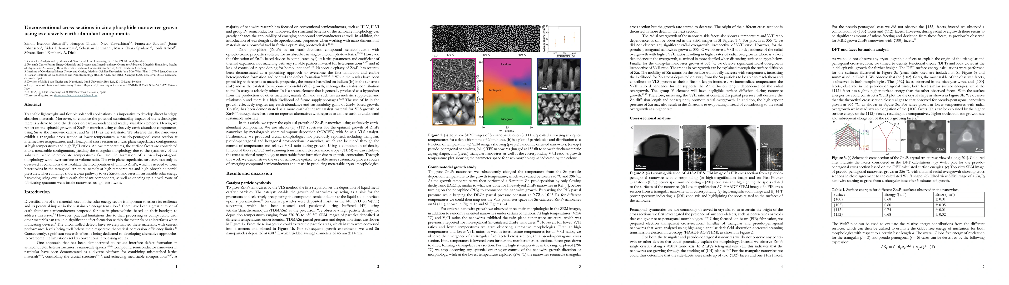
To enable lightweight and flexible solar cell applications it is imperative to develop direct bandgap absorber materials. Moreover, to enhance the potential sustainability impact of the technologies t...
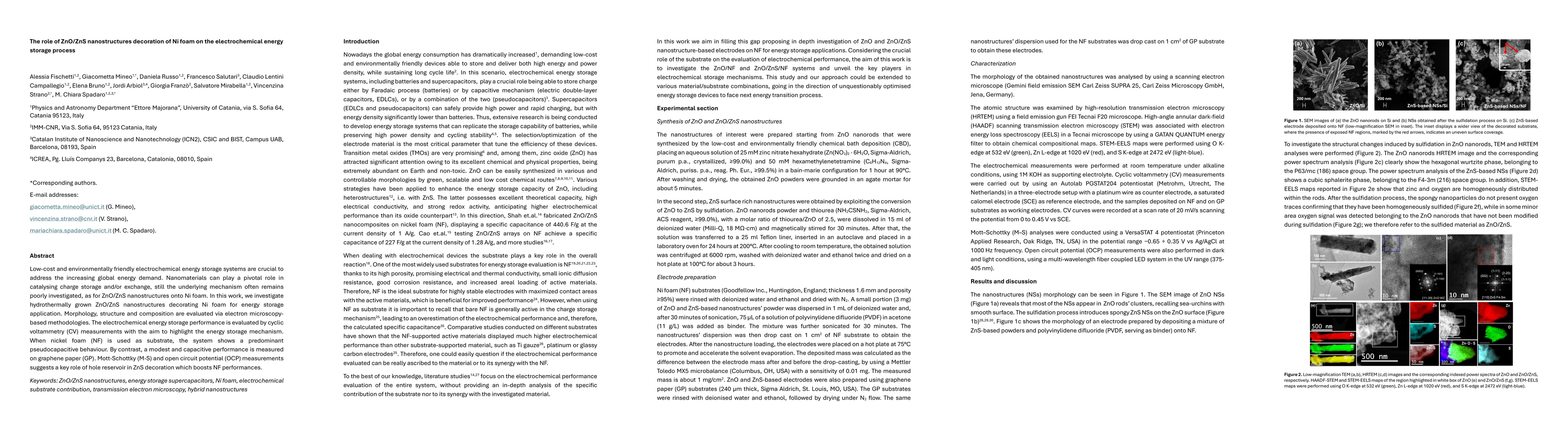
Low-cost and environmentally friendly electrochemical energy storage systems are crucial to address the increasing global energy demand. Nanomaterials can play a pivotal role in catalysing charge stor...
In superconductor-semiconductor hybrid structures, superconductivity and spin polarization are competing effects because magnetic fields break Cooper pairs. They can be combined using thin films and i...
Zinc phosphide (Zn3P2) is a promising photovoltaic absorber for thin-film and flexible solar cells due to its earth-abundant composition and favourable optoelectronic properties. Recent advances in ep...
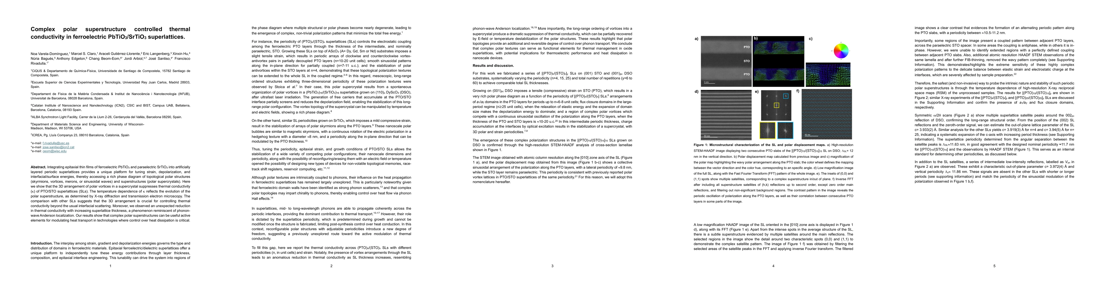
Integrating epitaxial thin films of ferroelectric PbTiO3 and paraelectric SrTiO3 into artificially layered periodic superlattices provides a unique platform for tuning strain, depolarization, and inte...