Academic Profile
Statistics
Similar Authors
Papers on arXiv
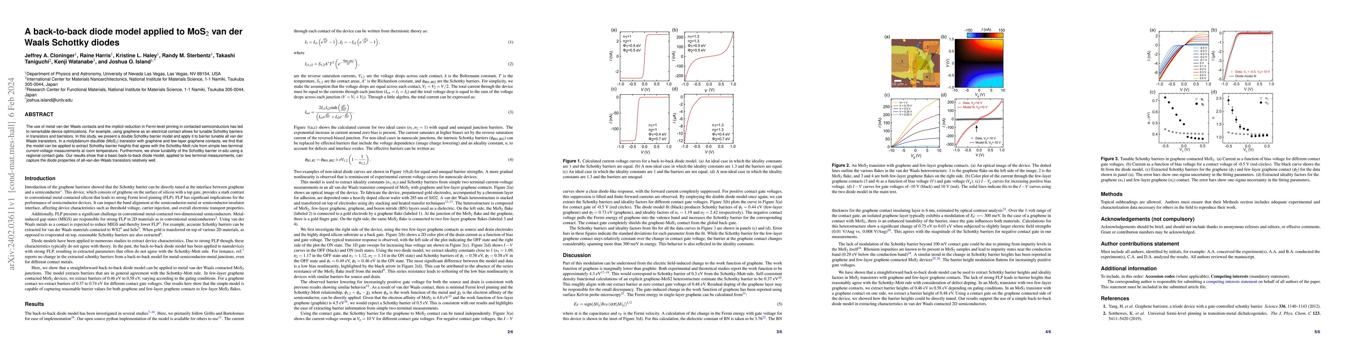
The use of metal van der Waals contacts and the implicit reduction in Fermi-level pinning in contacted semiconductors has led to remarkable device optimizations. For example, using graphene as an el...
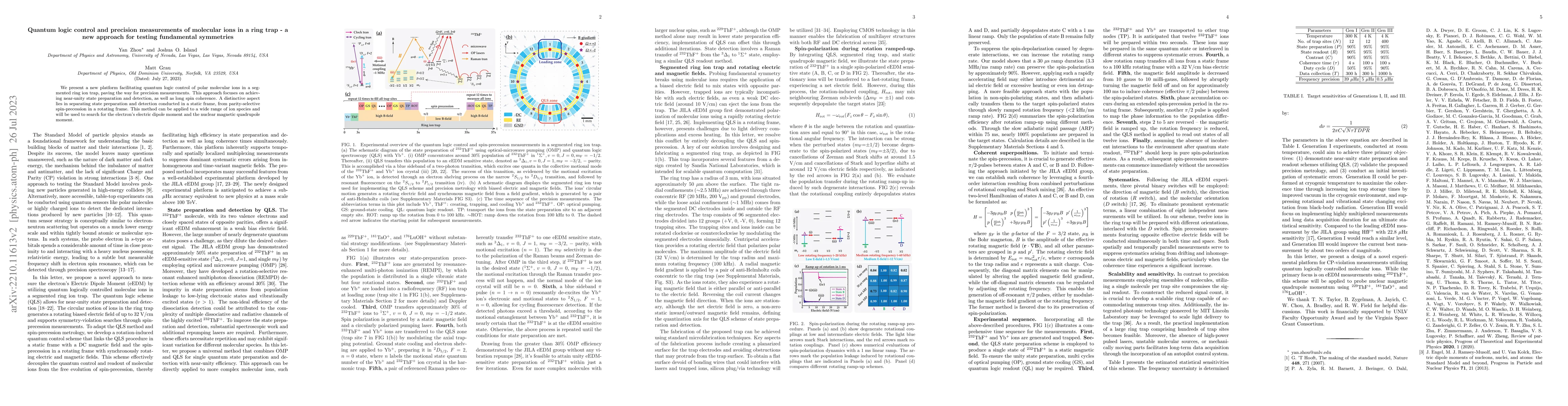
We present a new platform facilitating quantum logic control of polar molecular ions in a segmented ring ion trap, paving the way for precision measurements. This approach focuses on achieving near-...
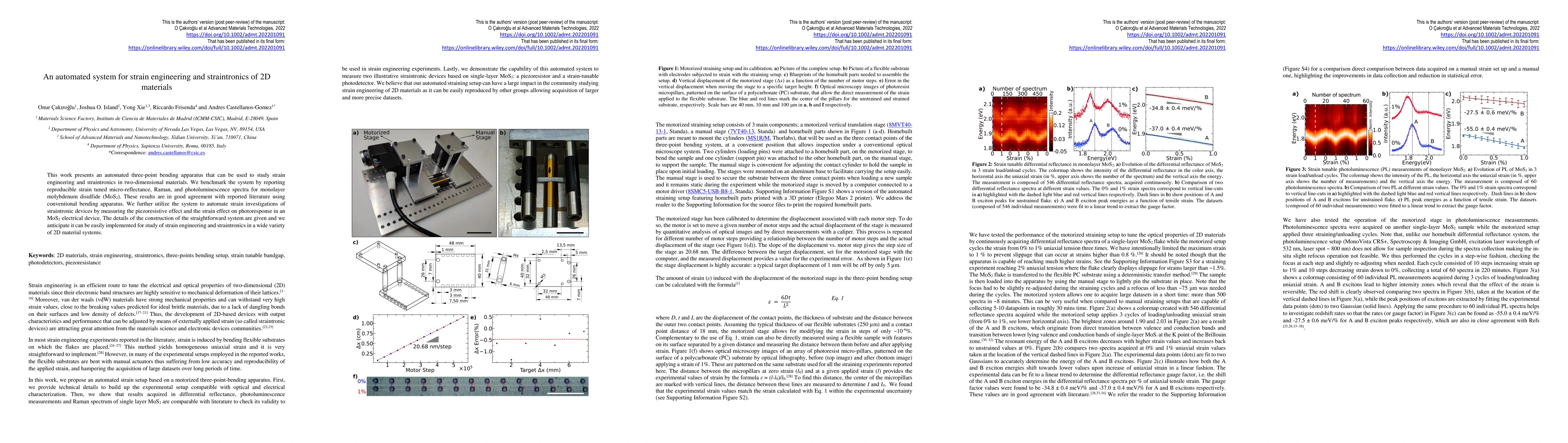
This work presents an automated three-point bending apparatus that can be used to study strain engineering and straintronics in two-dimensional materials. We benchmark the system by reporting reprod...
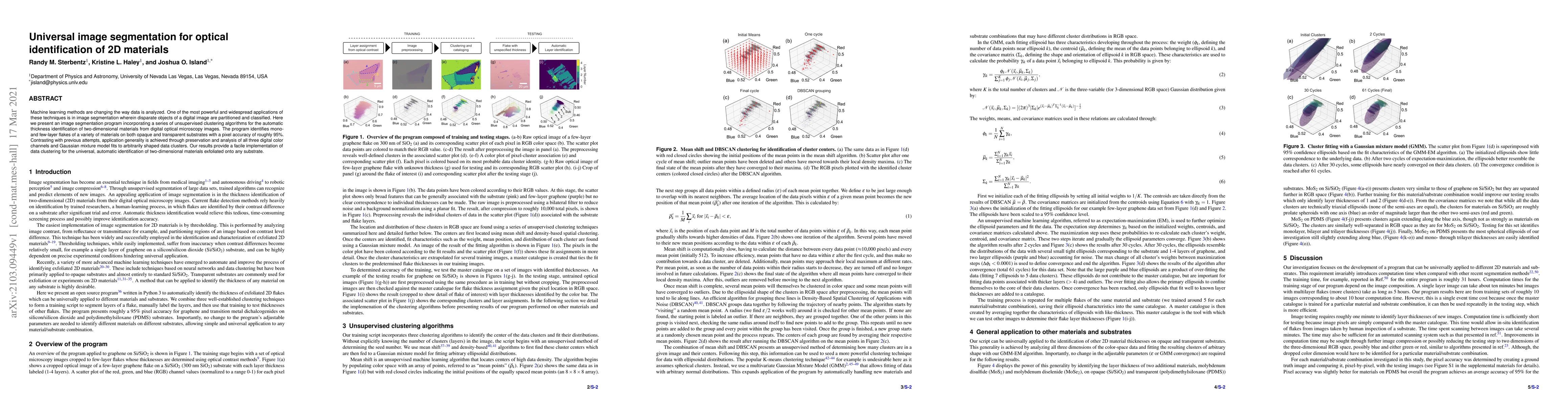
Machine learning methods are changing the way data is analyzed. One of the most powerful and widespread applications of these techniques is in image segmentation wherein disparate objects of a digit...
Two-dimensional layered trichalcogenide materials have recently attracted the attention of the scientific community because of its robust mechanical, thermal properties and applications in opto and ...
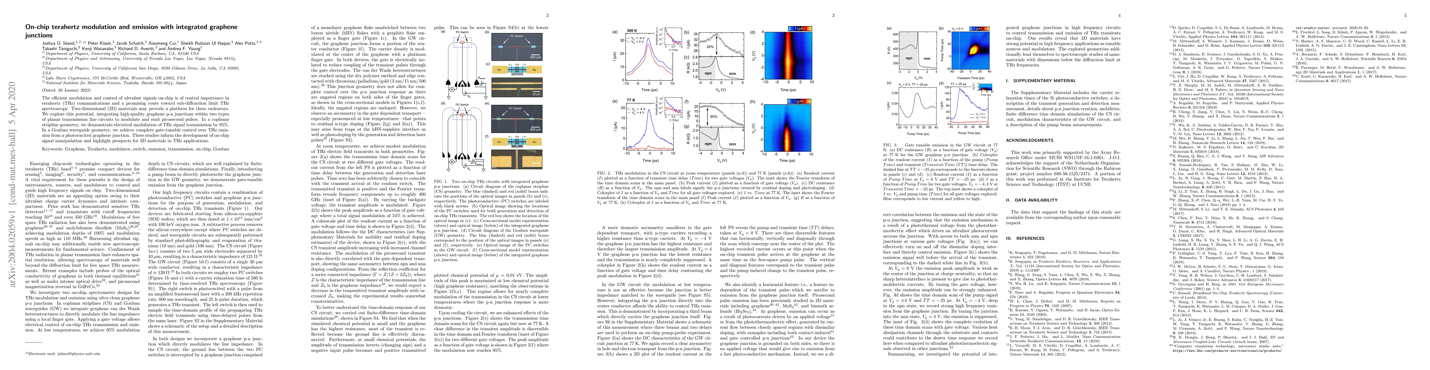
The efficient modulation and control of ultrafast signals on-chip is of central importance in terahertz (THz) communications and a promising route toward sub-diffraction limit THz spectroscopy. Two-...
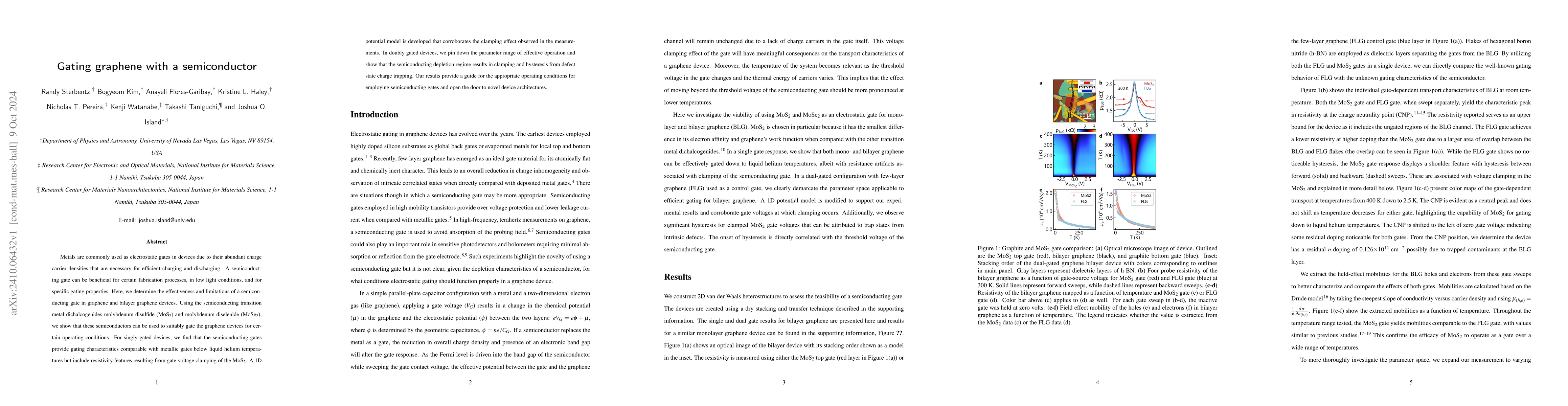
Metals are commonly used as electrostatic gates in devices due to their abundant charge carrier densities that are necessary for efficient charging and discharging. A semiconducting gate can be benefi...
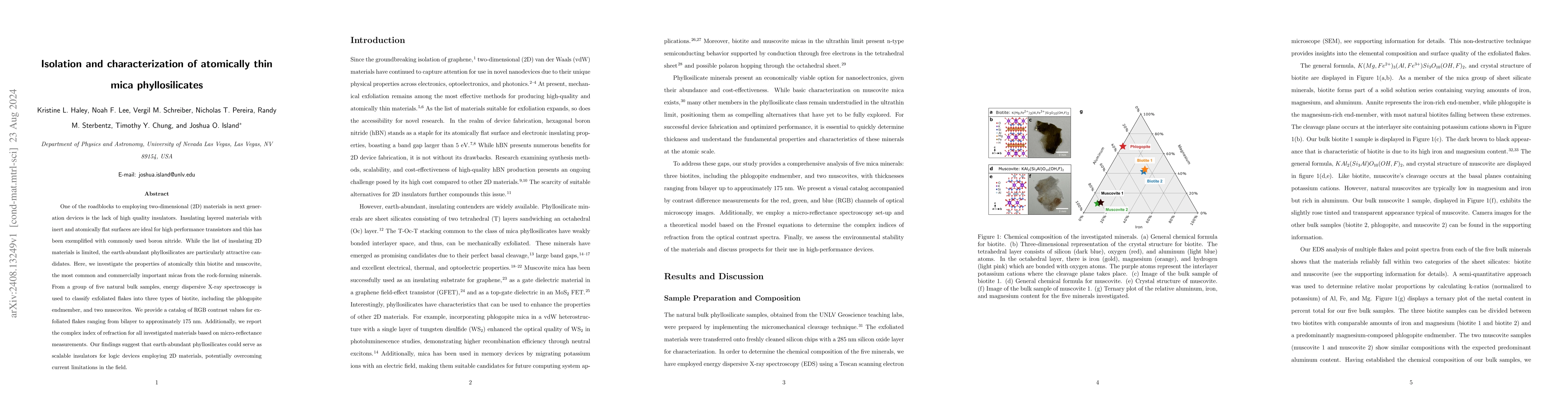
One of the roadblocks to employing two-dimensional (2D) materials in next generation devices is the lack of high quality insulators. Insulating layered materials with inert and atomically flat surface...