Academic Profile
Statistics
Similar Authors
Papers on arXiv
Monolithic active pixel sensors (MAPS) produced in a 65 nm CMOS imaging technology are being investigated for applications in particle physics. The MAPS design has a small collection electrode chara...
A reliable and cost-effective interconnect technology is required for the development of hybrid pixel detectors. The interconnect technology needs to be adapted for the pitch and die sizes of the re...
Within the ATTRACT FASTPIX project, a monolithic pixel sensor demonstrator chip has been developed in a modified 180 nm CMOS imaging process technology, targeting sub-nanosecond timing precision for...
Monolithic CMOS sensors in a 65 nm imaging technology are being investigated by the CERN EP Strategic R&D Programme on Technologies for Future Experiments for an application in particle physics. The...
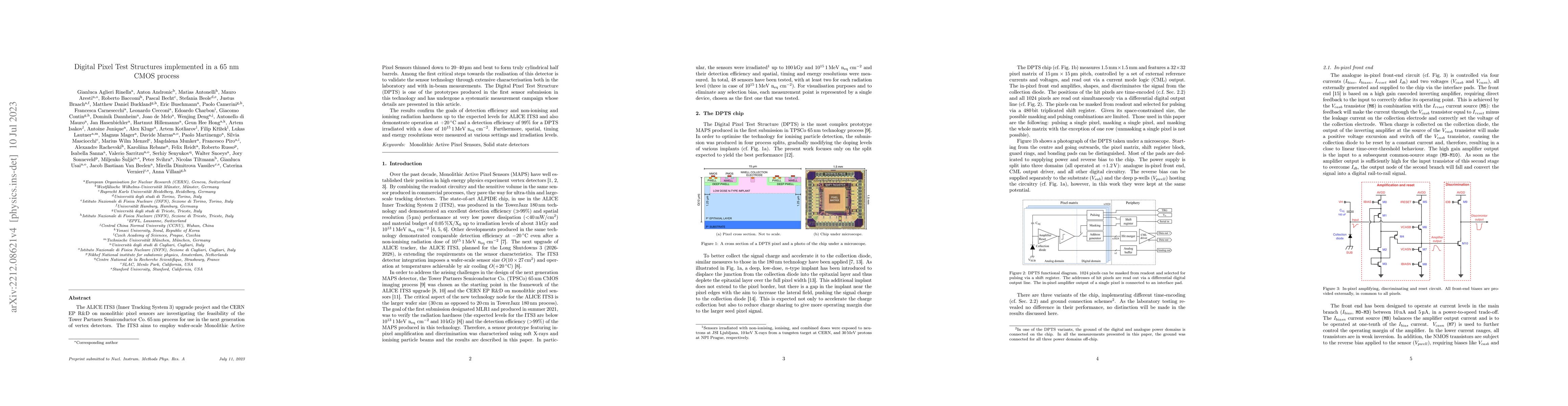
The ALICE ITS3 (Inner Tracking System 3) upgrade project and the CERN EP R&D on monolithic pixel sensors are investigating the feasibility of the Tower Partners Semiconductor Co. 65 nm process for u...
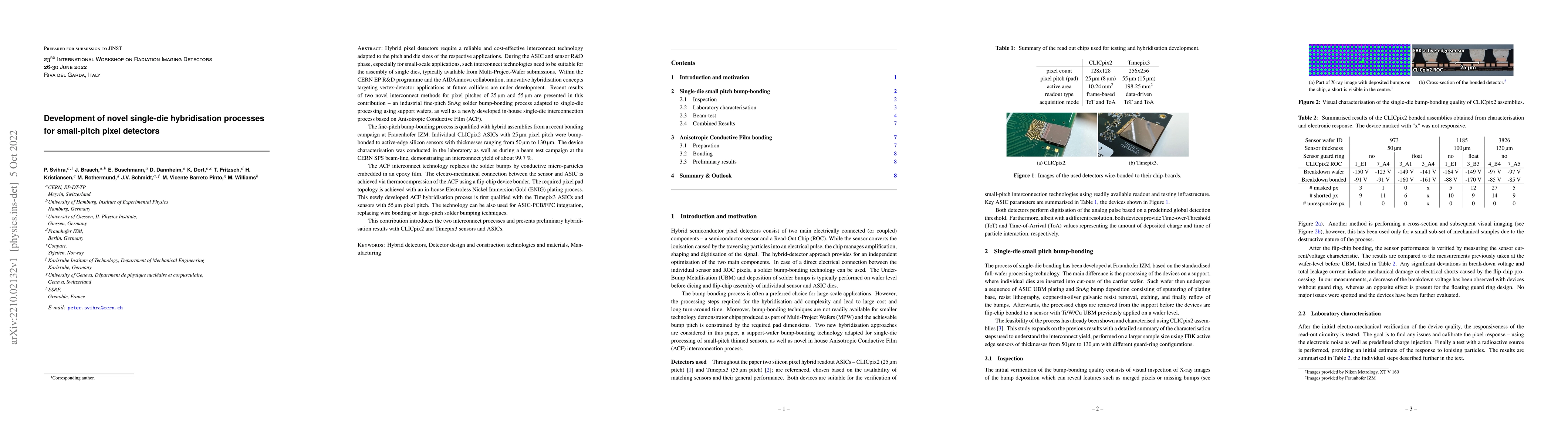
Hybrid pixel detectors require a reliable and cost-effective interconnect technology adapted to the pitch and die sizes of the respective applications. During the ASIC and sensor R\&D phase, especia...
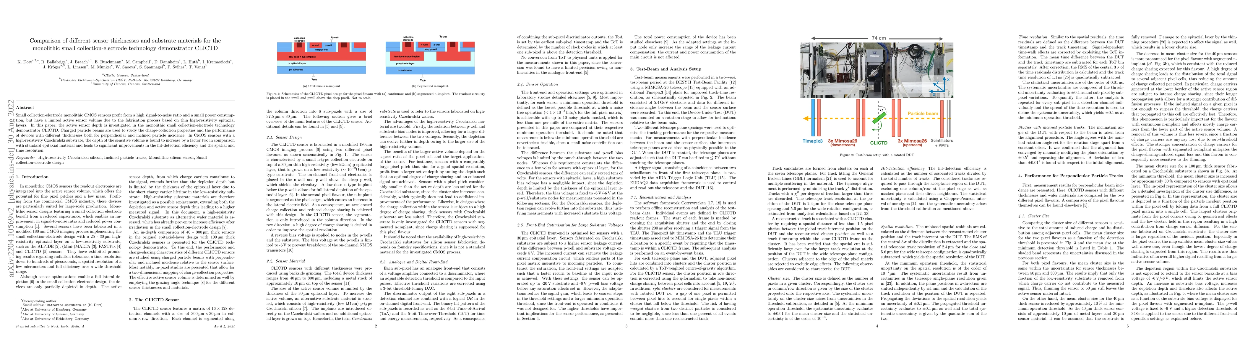
Small collection-electrode monolithic CMOS sensors profit from a high signal-to-noise ratio and a small power consumption, but have a limited active sensor volume due to the fabrication process base...
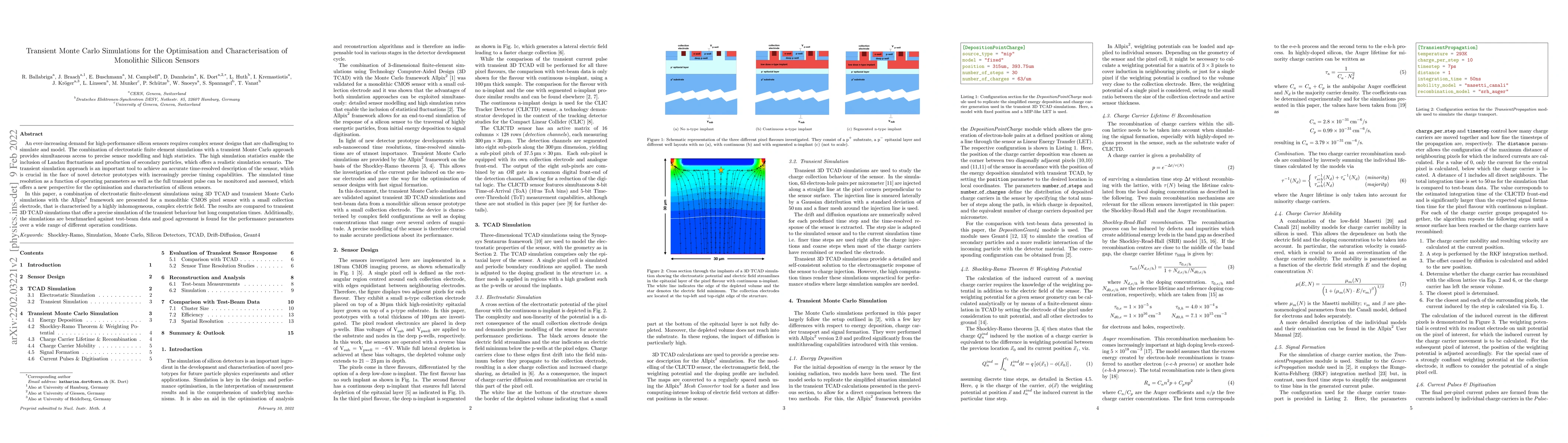
An ever-increasing demand for high-performance silicon sensors requires complex sensor designs that are challenging to simulate and model. The combination of electrostatic finite element simulations...
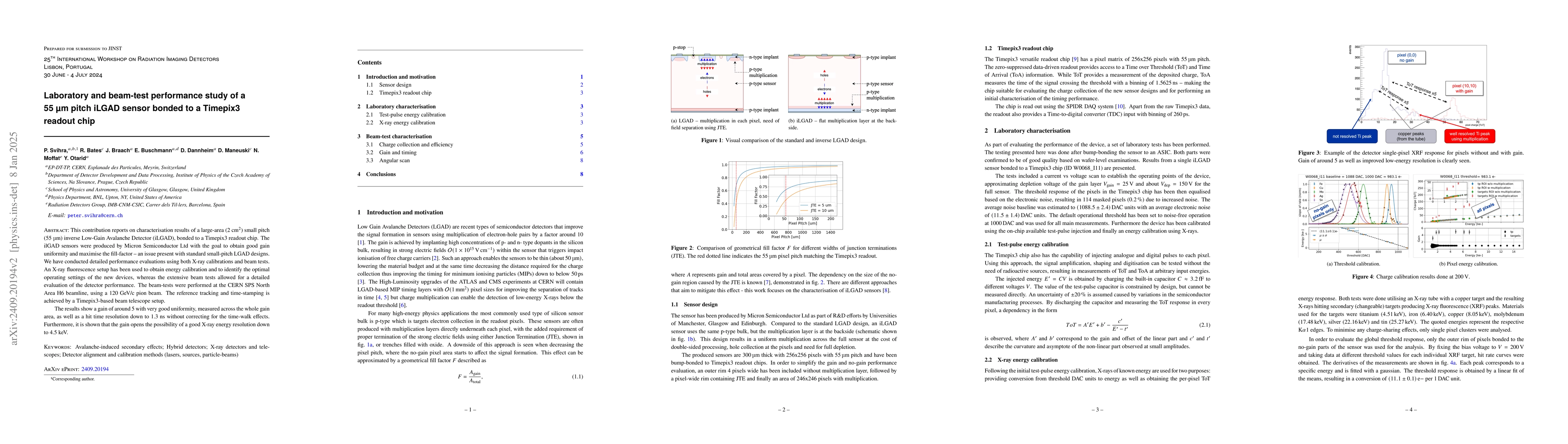
This contribution reports on characterisation results of a large-area (2$~\mathrm{cm}^2$) small pitch (55$~\mu$m) inverse Low-Gain Avalanche Detector (iLGAD), bonded to a Timepix3 readout chip. The il...
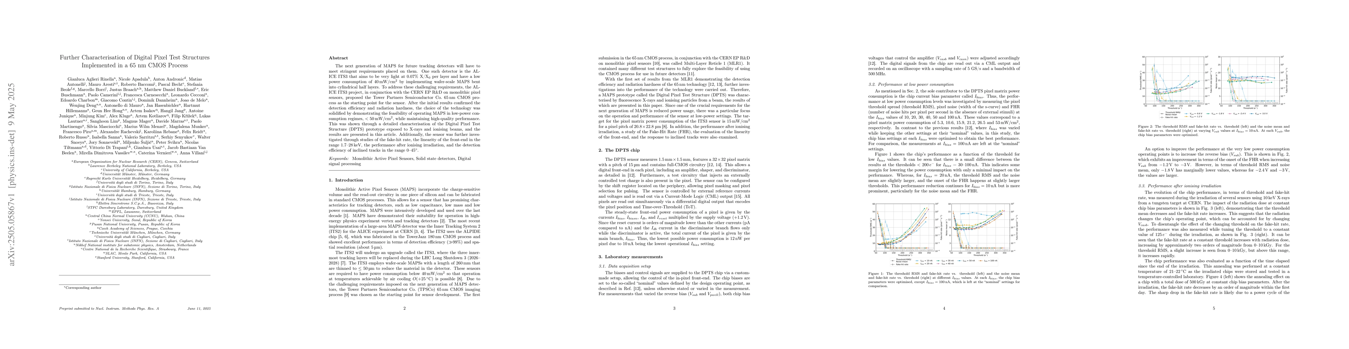
The next generation of MAPS for future tracking detectors will have to meet stringent requirements placed on them. One such detector is the ALICE ITS3 that aims to be very light at 0.07% X/X$_{0}$ per...
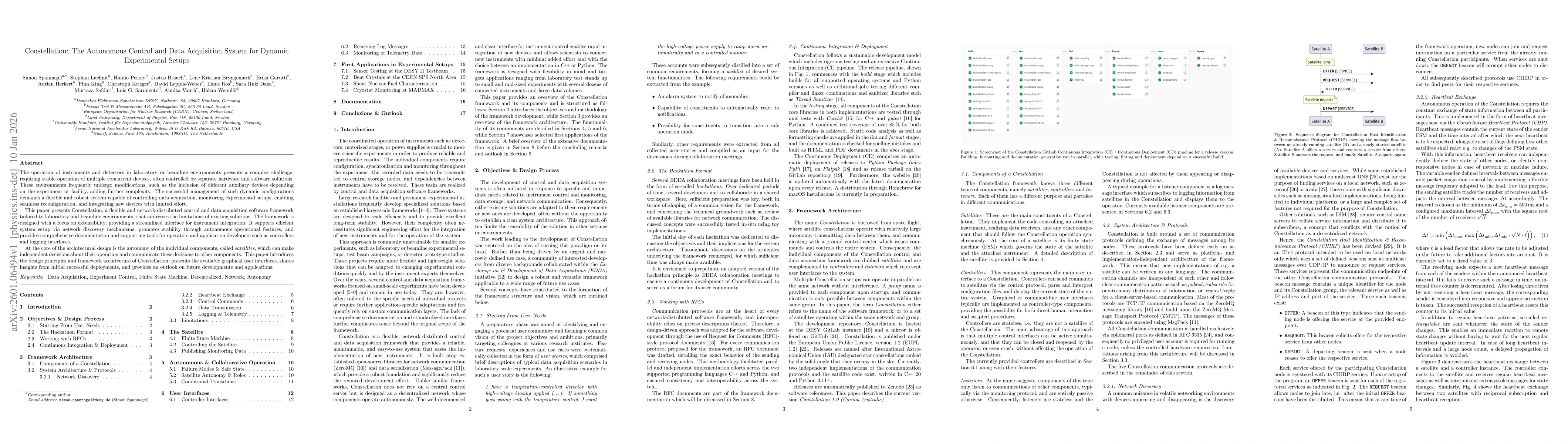
The operation of instruments and detectors in laboratory or beamline environments presents a complex challenge, requiring stable operation of multiple concurrent devices, often controlled by separate ...