ArxivLens
K
Researcher

K. Nagashio

8 papers on arXiv

8 arXiv Papers
2 Total Publications
Profile

Academic Profile

Name K. Nagashio
Total Papers 2
Scholar Profile View on Semantic Scholar
Metrics

Statistics

8 arXiv Papers
2 Total Publications
Publications

Papers on arXiv

Thumbnail for Room-temperature quantum emission from interface excitons in
  mixed-dimensional heterostructures
arXiv
Room-temperature quantum emission from interface excitons in mixed-dimensional heterostructures

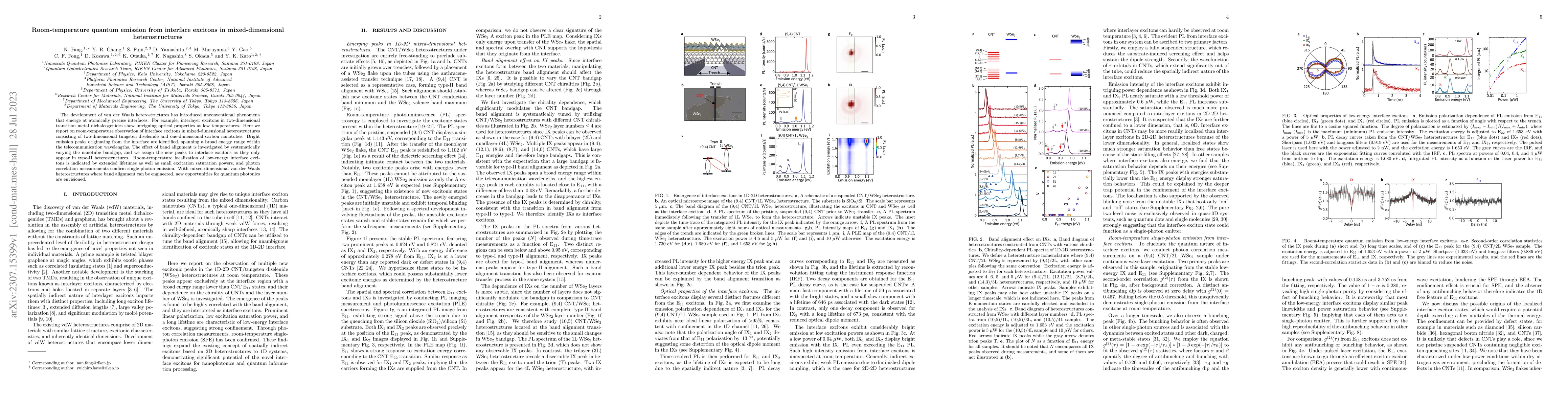
The development of van der Waals heterostructures has introduced unconventional phenomena that emerge at atomically precise interfaces. For example, interlayer excitons in two-dimensional transition...

Thumbnail for Resonant exciton transfer in mixed-dimensional heterostructures for
  overcoming dimensional restrictions in optical processes
arXiv
Resonant exciton transfer in mixed-dimensional heterostructures for overcoming dimensional restrictions in optical processes

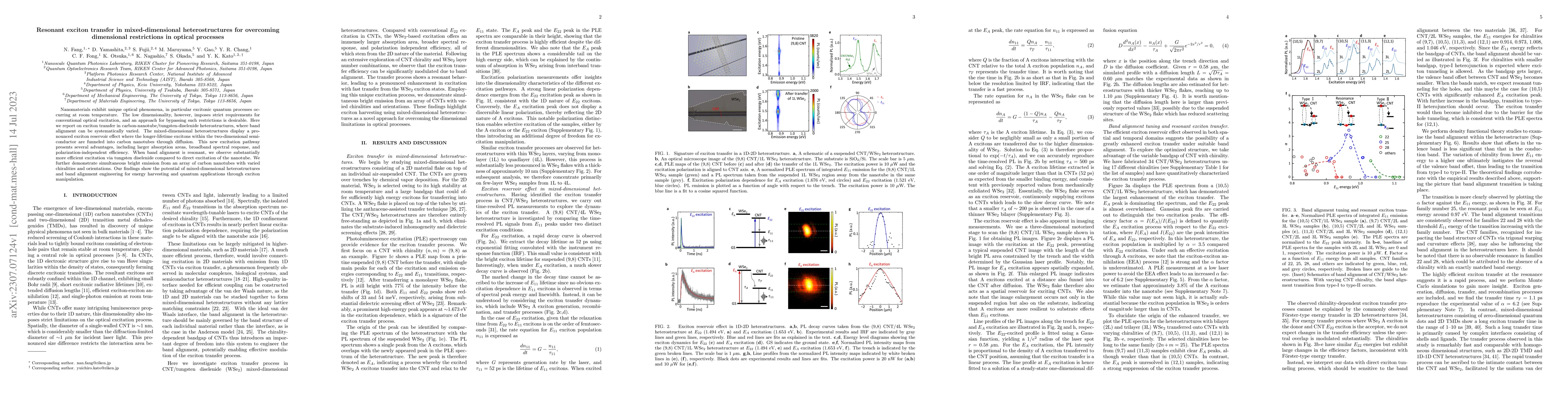
Nanomaterials exhibit unique optical phenomena, in particular excitonic quantum processes occurring at room temperature. The low dimensionality, however, imposes strict requirements for conventional...

Thumbnail for Quantization of mode shifts in nanocavities integrated with atomically
  thin sheets
arXiv
Quantization of mode shifts in nanocavities integrated with atomically thin sheets

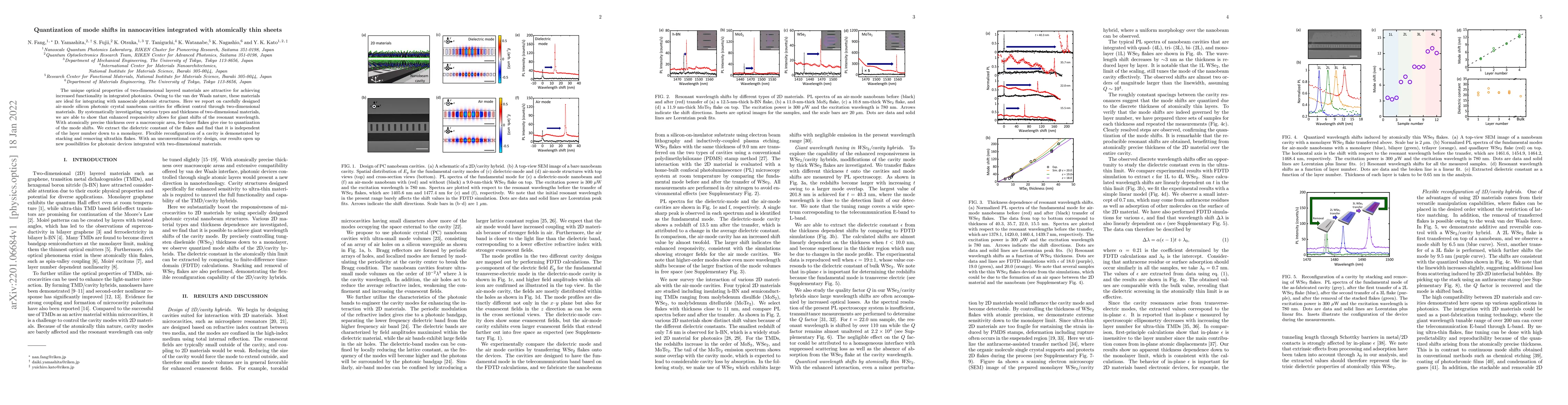
The unique optical properties of two-dimensional layered materials are attractive for achieving increased functionality in integrated photonics. Owing to the van der Waals nature, these materials ar...

Thumbnail for Micrometer-scale monolayer SnS growth by physical vapor deposition
arXiv
Micrometer-scale monolayer SnS growth by physical vapor deposition

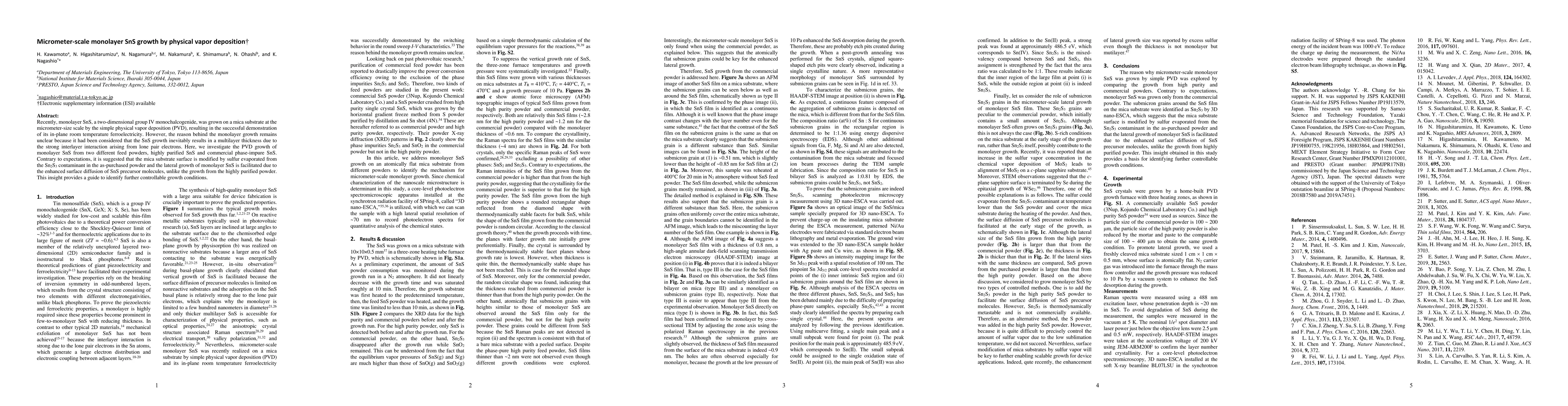
Recently, monolayer SnS, a two-dimensional group IV monochalcogenide, was grown on a mica substrate at the micrometer-size scale by the simple physical vapor deposition (PVD), resulting in the succe...

Thumbnail for Purely in-plane ferroelectricity in monolayer SnS at room temperature
arXiv
Purely in-plane ferroelectricity in monolayer SnS at room temperature

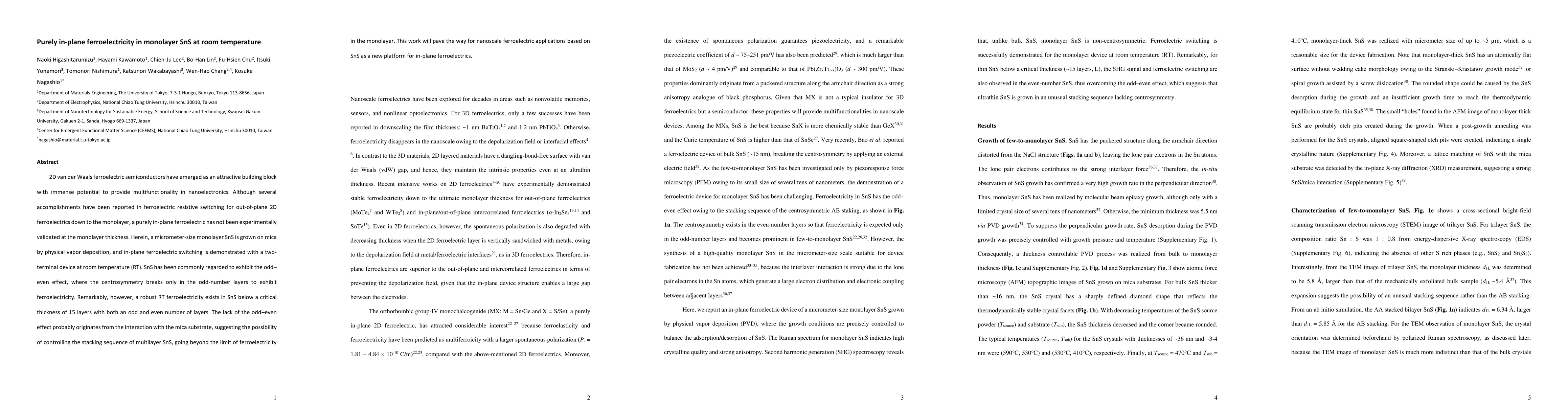
2D van der Waals ferroelectric semiconductors have emerged as an attractive building block with immense potential to provide multifunctionality in nanoelectronics. Although several accomplishments h...

Thumbnail for Full energy spectra of interface state densities for n- and p-type MoS2
  field-effect transistors
arXiv
Full energy spectra of interface state densities for n- and p-type MoS2 field-effect transistors

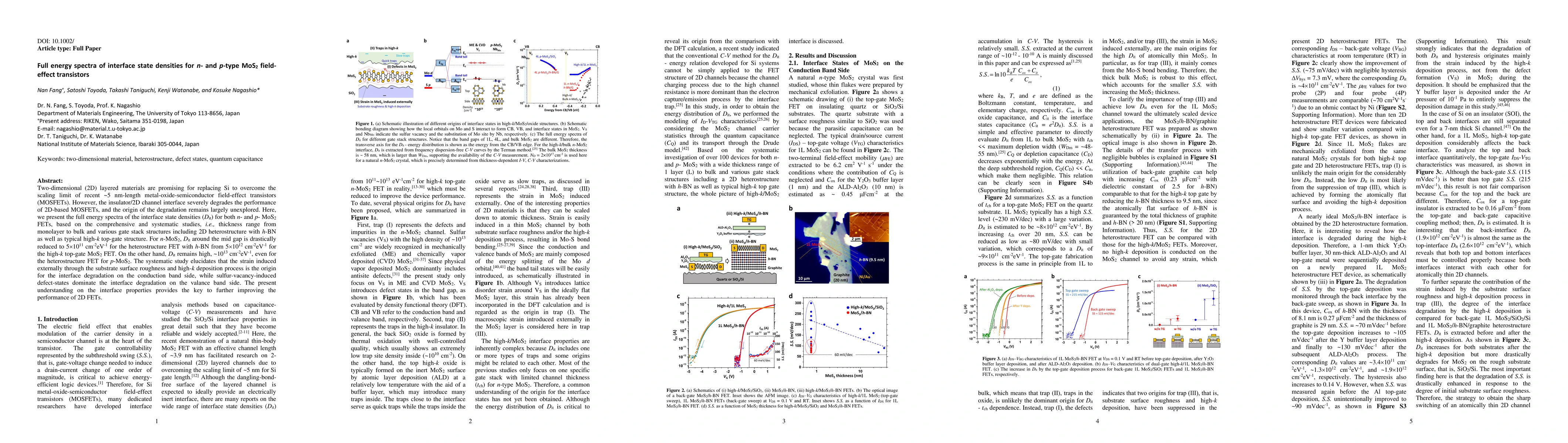
Two-dimensional (2D) layered materials are promising for replacing Si to overcome the scaling limit of recent ~5 nm-length metal-oxide-semiconductor field-effect transistors (MOSFETs). However, the ...

Thumbnail for Hexagonal boron nitride as an ideal substrate for carbon nanotube
  photonics
arXiv
Hexagonal boron nitride as an ideal substrate for carbon nanotube photonics

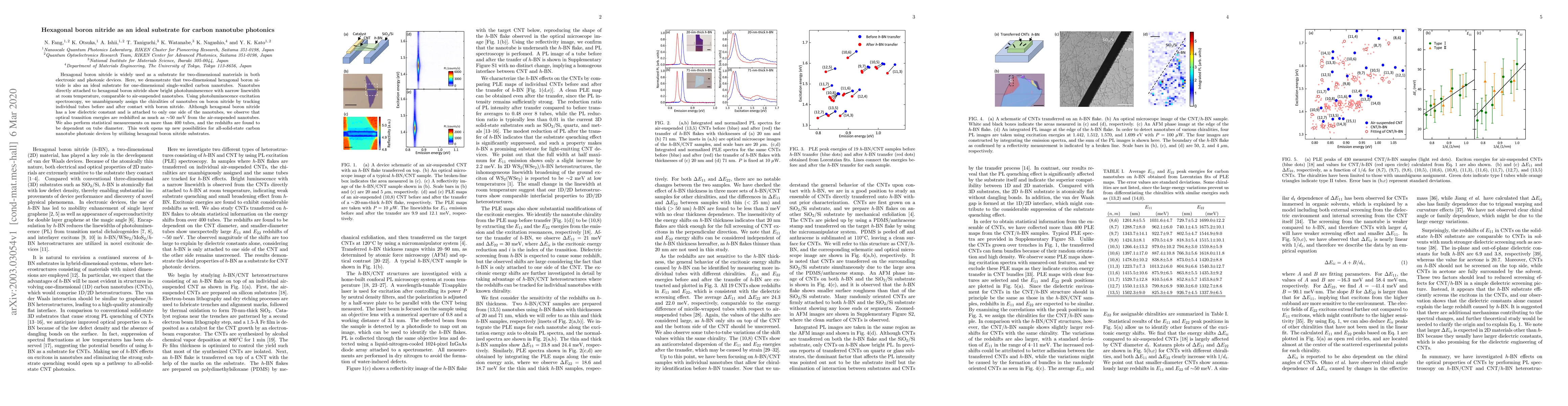
Hexagonal boron nitride is widely used as a substrate for two-dimensional materials in both electronic and photonic devices. Here, we demonstrate that two-dimensional hexagonal boron nitride is also...

Thumbnail for Trion transfer in mixed-dimensional heterostructures
arXiv
Trion transfer in mixed-dimensional heterostructures

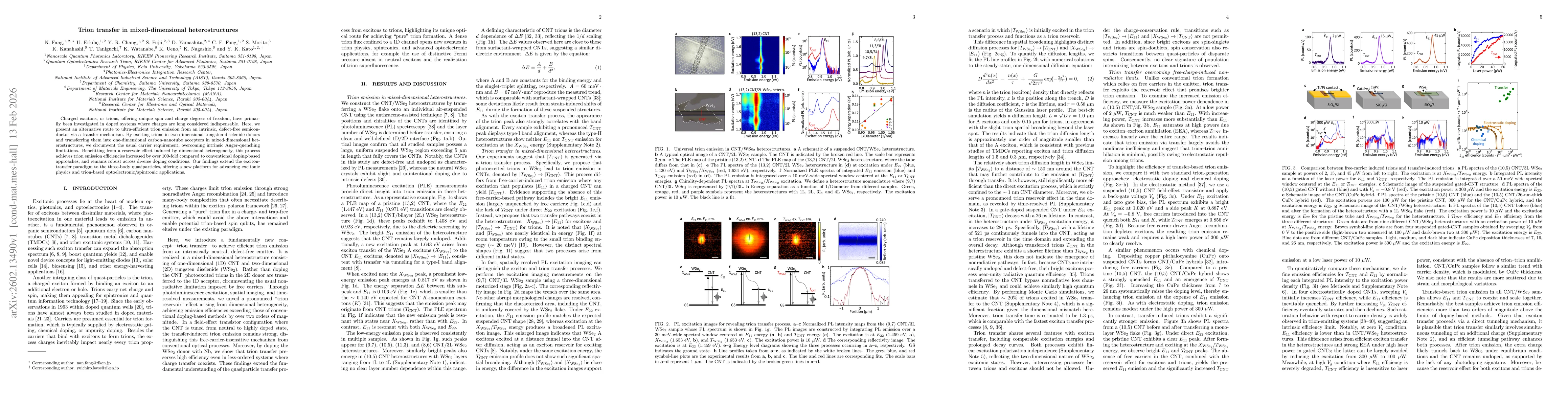
Charged excitons, or trions, offering unique spin and charge degrees of freedom, have primarily been investigated in doped systems where charges are long considered indispensable. Here, we present an ...

This website uses cookies to ensure you get the best experience. Learn more