Academic Profile
Statistics
Similar Authors
Papers on arXiv
Moire superlattices formed in van der Waals heterostructures due to twisting, lattice mismatch and strain present an opportunity for creating novel metamaterials with unique properties not present i...
Van der Waals electrode integration is a promising strategy to create near-perfect interfaces between metals and two-dimensional materials, with advantages such as eliminating Fermi-level pinning an...
The remarkable electrical, optical and mechanical properties of graphene make it a desirable material for electronics, optoelectronics and quantum applications. A fundamental understanding of the el...
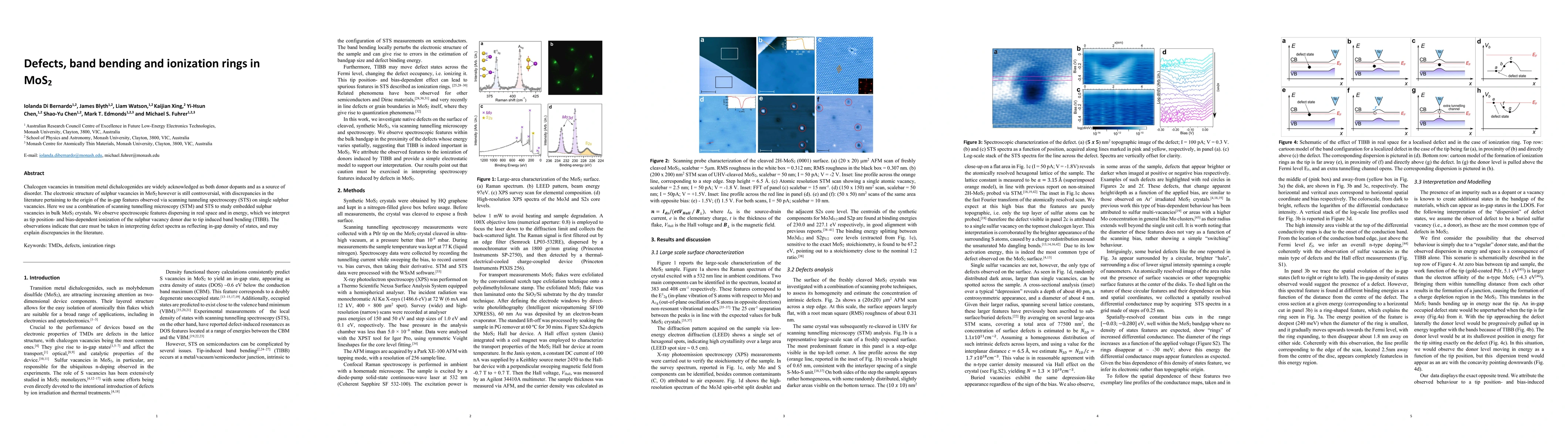
Chalcogen vacancies in transition metal dichalcogenides are widely acknowledged as both donor dopants and as a source of disorder. The electronic structure of sulphur vacancies in MoS2 however is st...
1 School of Physics and Astronomy, Monash University, Clayton, Victoria 3800, Australia 2 Australian Research Council Centre of Excellence in Future Low-Energy Electronics Technologies (FLEET), Mona...
Two-dimensional (2D) platinum diselenide (PtSe$_2$) has received significant attention for 2D transistor applications due to its high mobility. Here, using molecular beam epitaxy, we investigate the...
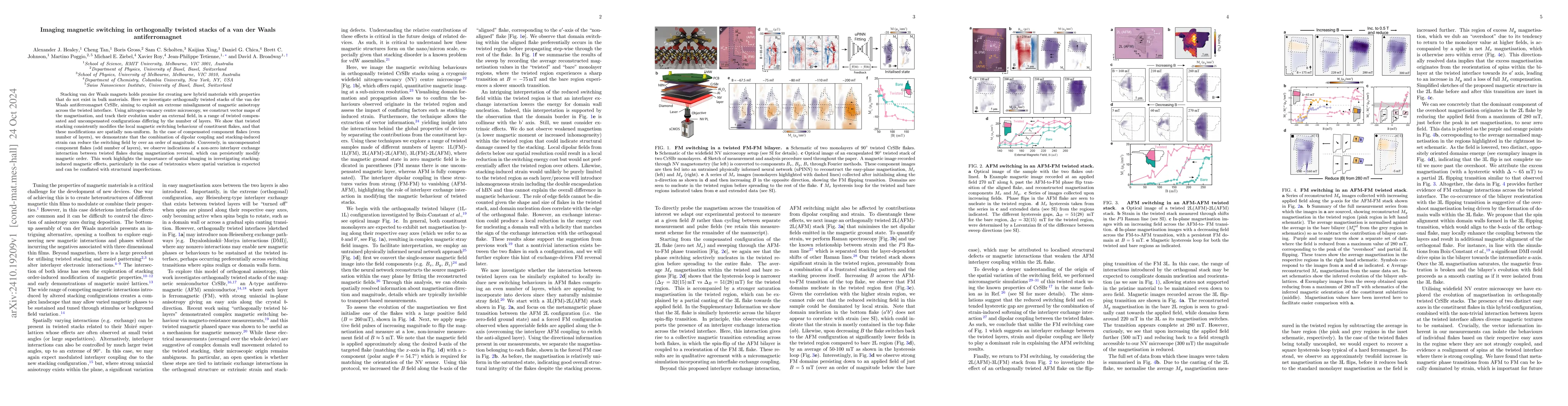
Stacking van der Waals magnets holds promise for creating new hybrid materials with properties that do not exist in bulk materials. Here we investigate orthogonally twisted stacks of the van der Waals...
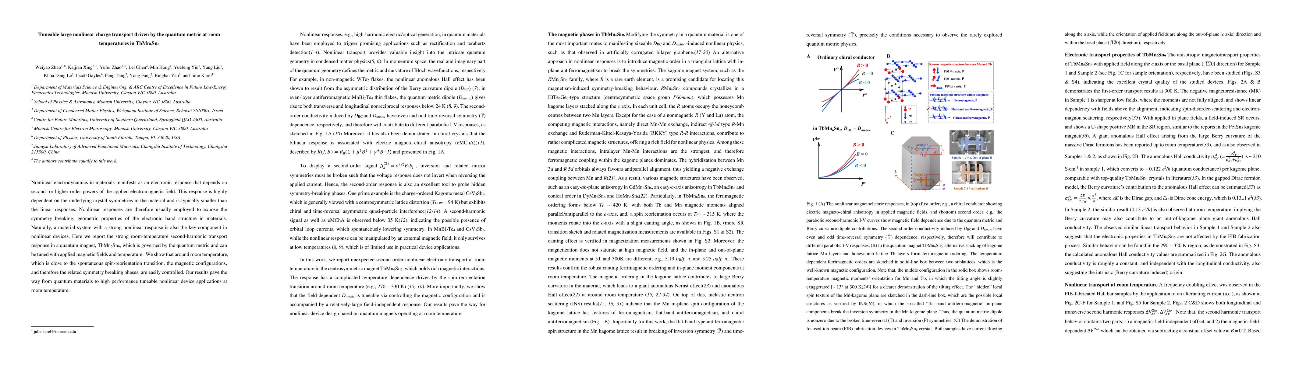
Nonlinear electrodynamics in materials manifests as an electronic response that depends on second- or higher-order powers of the applied electromagnetic field. This response is highly dependent on the...
In transition metal dichalcogenides, the valley degree of freedom directly couples valley-polarised excitons - excited by circularly polarised light - to valley-dependent chiral photons, enabling ultr...
Hexagonal boron nitride (hBN) has recently been shown to host native defects exhibiting optically detected magnetic resonance (ODMR) with applications in nanoscale magnetic sensing and imaging. To adv...
The development of advanced electronic devices is contingent upon sustainable material development and pioneering research breakthroughs. Traditional semiconductor-based electronic technology faces co...
Twisted transition-metal dichalcogenides host highly tunable moiré potentials, flat bands, and correlated electronic phases, yet the role of disorder in shaping these emergent properties remains large...
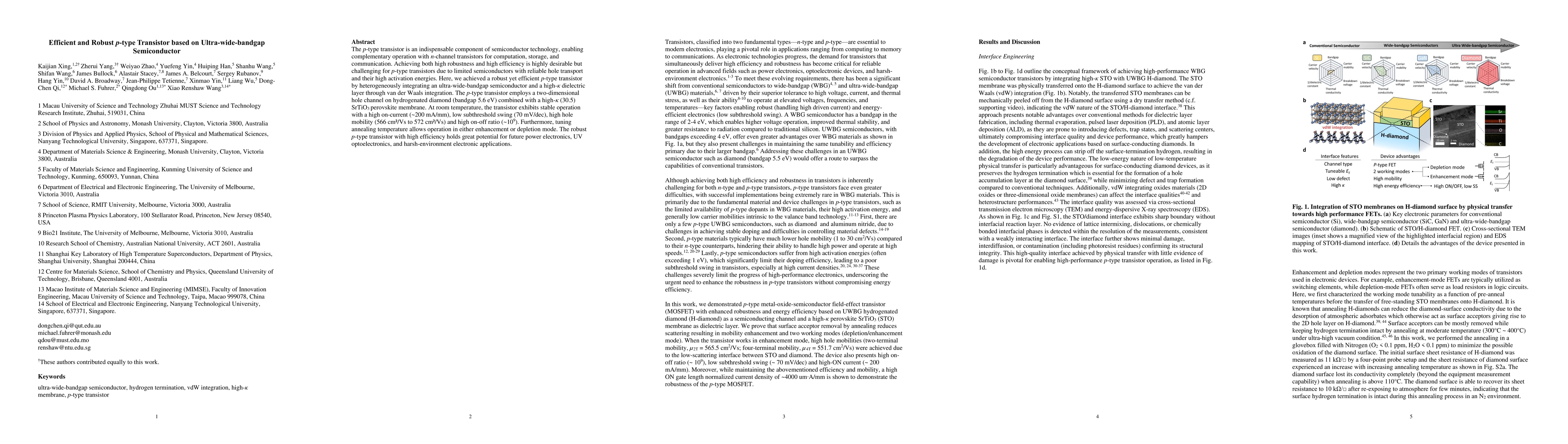
The p-type transistor is an indispensable component of semiconductor technology, enabling complementary operation with n-channel transistors for computation, storage, and communication. Achieving both...
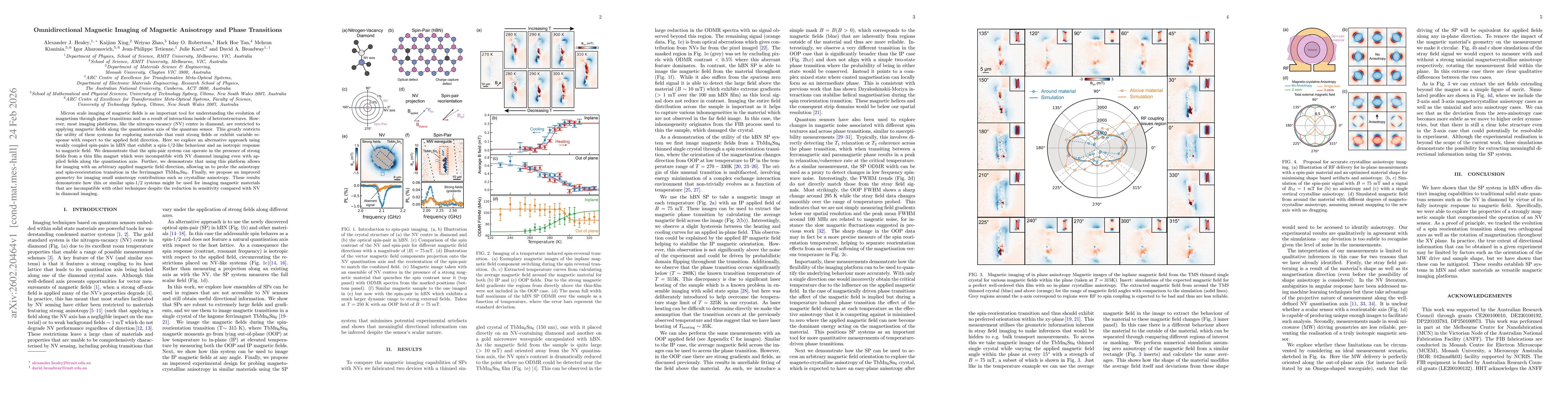
Micron scale imaging of magnetic fields is an important tool for understanding the evolution of magnetism through phase transitions and as a result of interactions inside of heterostructures. However,...
The observation of strong and tunable spin-orbit interaction (SOI) in surface conducting diamond opens up a new avenue for building diamond-based spintronics. Herein we provide a comprehensive method ...