Katherine A. Cochrane

7 papers on arXiv

Academic Profile

Name: K. Cochrane
Total Papers: 23

Statistics

arXiv Papers 7
Total Publications 23

Papers on arXiv

Thumbnail for Designing optoelectronic properties by on-surface synthesis: formation
  and electronic structure of an iron-terpyridine macromolecular complex

Designing optoelectronic properties by on-surface synthesis: formation and electronic structure of an iron-terpyridine macromolecular complex

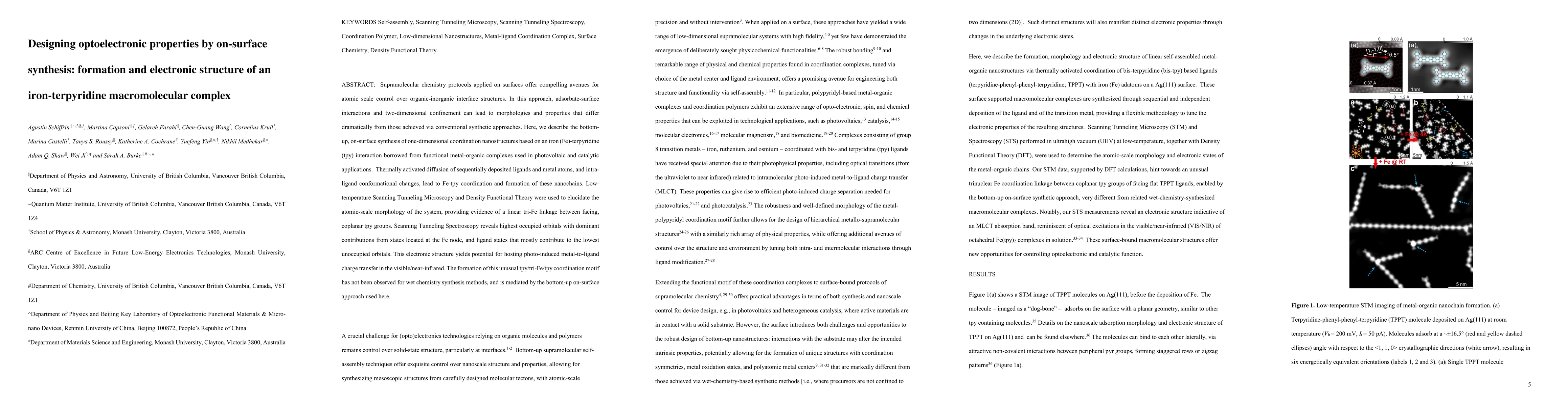
Supramolecular chemistry protocols applied on surfaces offer compelling avenues for atomic scale control over organic-inorganic interface structures. In this approach, adsorbate-surface interactions...

Thumbnail for Molecularly Resolved Electronic Landscapes of Differing Acceptor-Donor
  Interface Geometries

Molecularly Resolved Electronic Landscapes of Differing Acceptor-Donor Interface Geometries

Organic semiconductors are a promising class of materials for numerous electronic and optoelectronic applications, including solar cells. However, these materials tend to be extremely sensitive to t...

Thumbnail for Vibronic response of a spin-1/2 state from a carbon impurity in
  two-dimensional WS$_2$

Vibronic response of a spin-1/2 state from a carbon impurity in two-dimensional WS$_2$

We demonstrate the creation of a spin-1/2 state via the atomically controlled generation of magnetic carbon radical ions (CRIs) in synthetic two-dimensional transition metal dichalcogenides (TMDs). ...

Thumbnail for How Substitutional Point Defects in Two-Dimensional WS$_2$ Induce Charge
  Localization, Spin-Orbit Splitting, and Strain

How Substitutional Point Defects in Two-Dimensional WS$_2$ Induce Charge Localization, Spin-Orbit Splitting, and Strain

Control of impurity concentrations in semiconducting materials is essential to device technology. Because of their intrinsic confinement, the properties of two-dimensional semiconductors such as tra...

Thumbnail for Electrically driven photon emission from individual atomic defects in
  monolayer WS2

Electrically driven photon emission from individual atomic defects in monolayer WS2

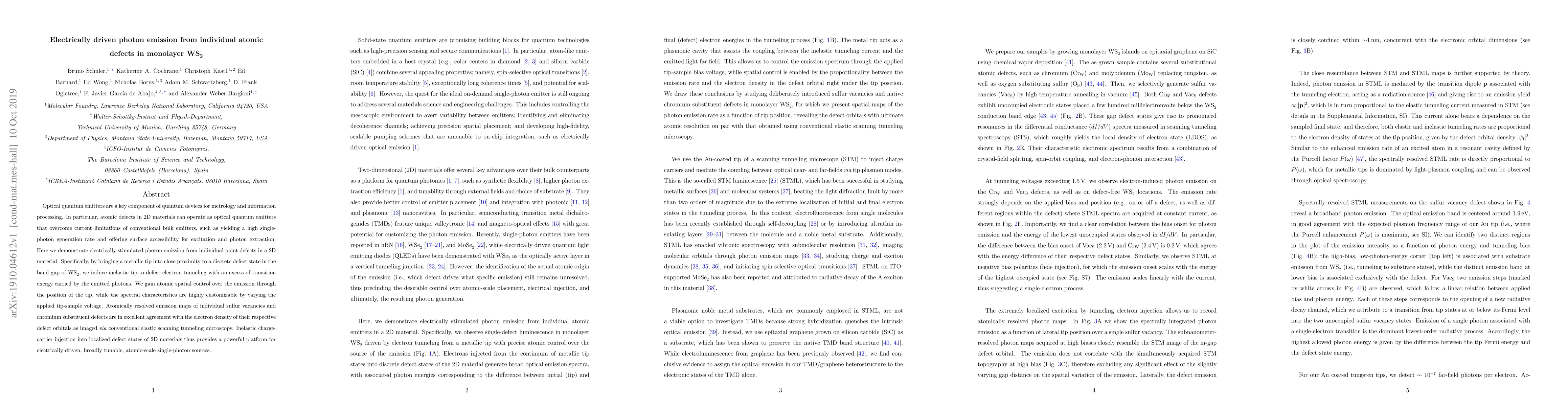
Optical quantum emitters are a key component of quantum devices for metrology and information processing. In particular, atomic defects in 2D materials can operate as optical quantum emitters that o...

Thumbnail for Resonant and Bound States of Charged Defects in Two-Dimensional
  Semiconductors

Resonant and Bound States of Charged Defects in Two-Dimensional Semiconductors

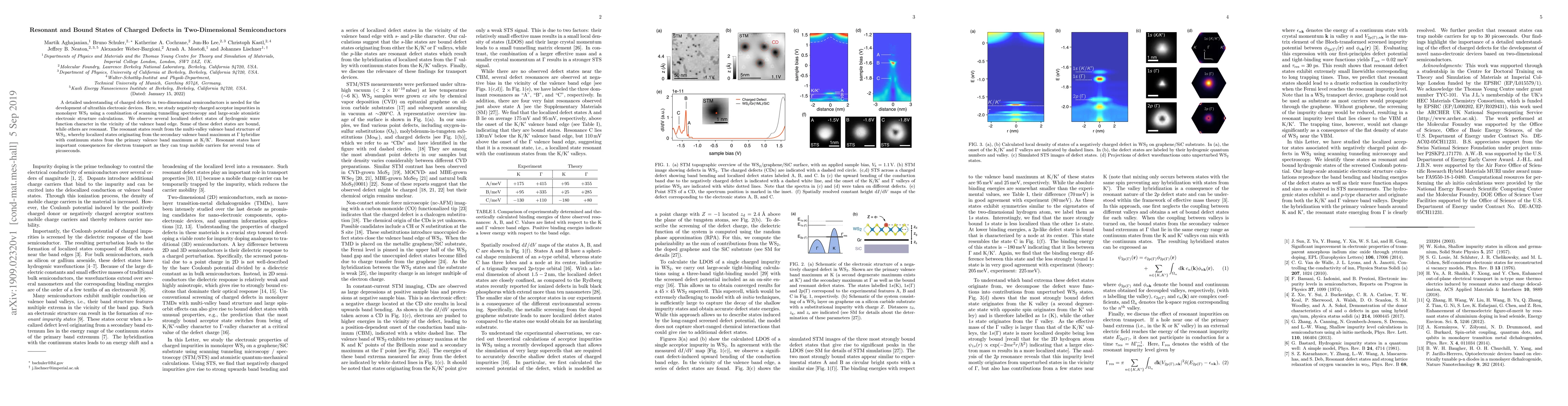
A detailed understanding of charged defects in two-dimensional semiconductors is needed for the development of ultrathin electronic devices. Here, we study negatively charged acceptor impurities in ...

Thumbnail for Extended Hubbard Model realized in 2D clusters of molecular anions

Extended Hubbard Model realized in 2D clusters of molecular anions

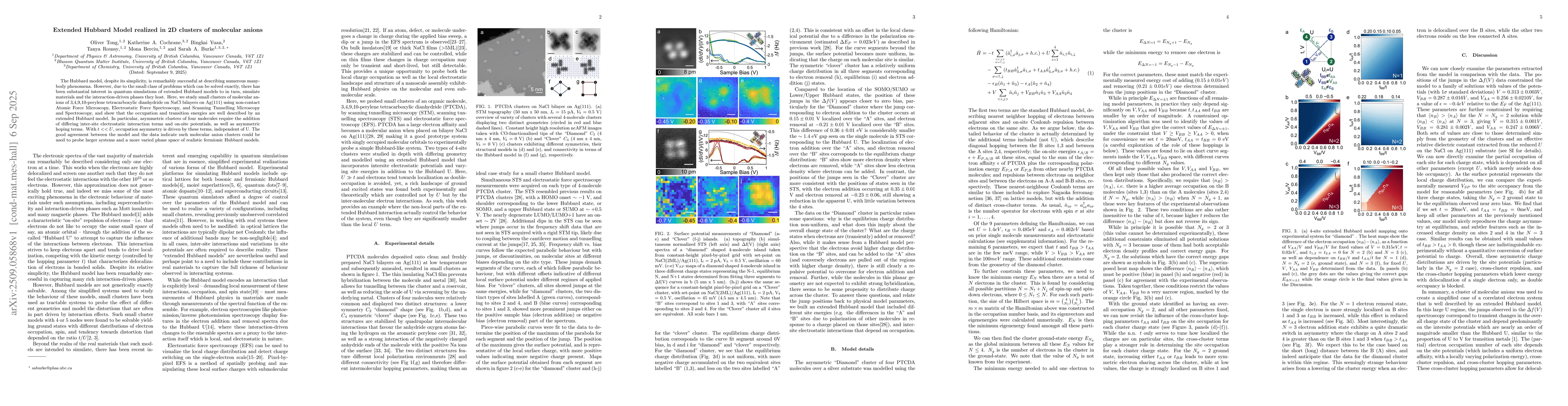
The Hubbard model, despite its simplicity, is remarkably successful at describing numerous many-body phenomena. However, due to the small class of problems which can be solved exactly, there has been ...

This website uses cookies to ensure you get the best experience. Learn more