Academic Profile
Statistics
Similar Authors
Papers on arXiv
Electrostatic modification of functional materials by electrolytic gating has demonstrated a remarkably wide range of density modulation, a condition crucial for developing novel electronic phases i...
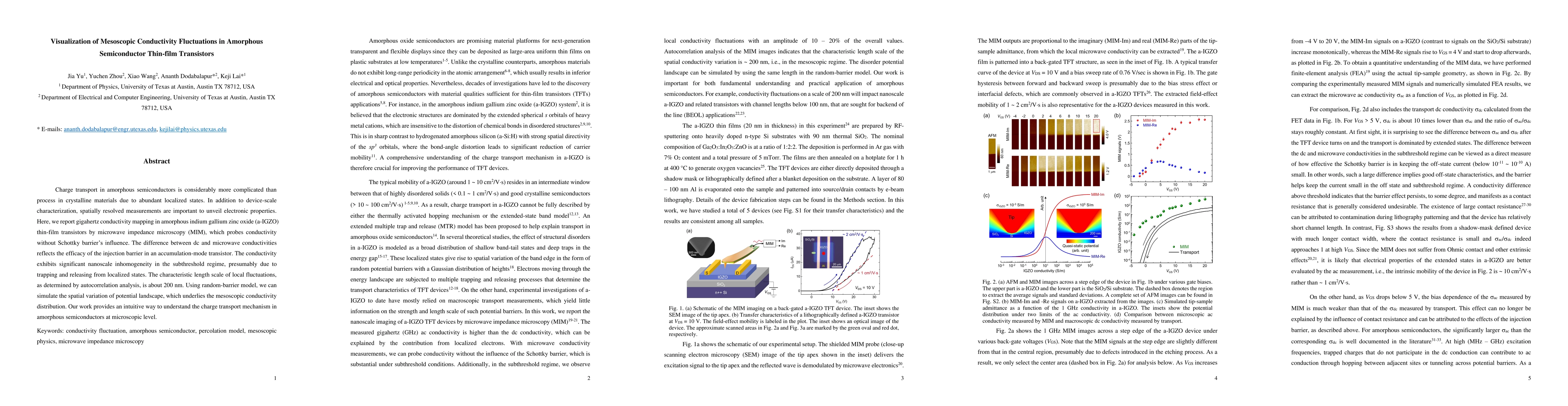
Charge transport in amorphous semiconductors is considerably more complicated than process in crystalline materials due to abundant localized states. In addition to device-scale characterization, sp...
Moir\'e superlattices formed by vertically stacking van der Waals layers host a rich variety of correlated electronic phases and function as novel photonic materials. The moir\'e potential of the su...
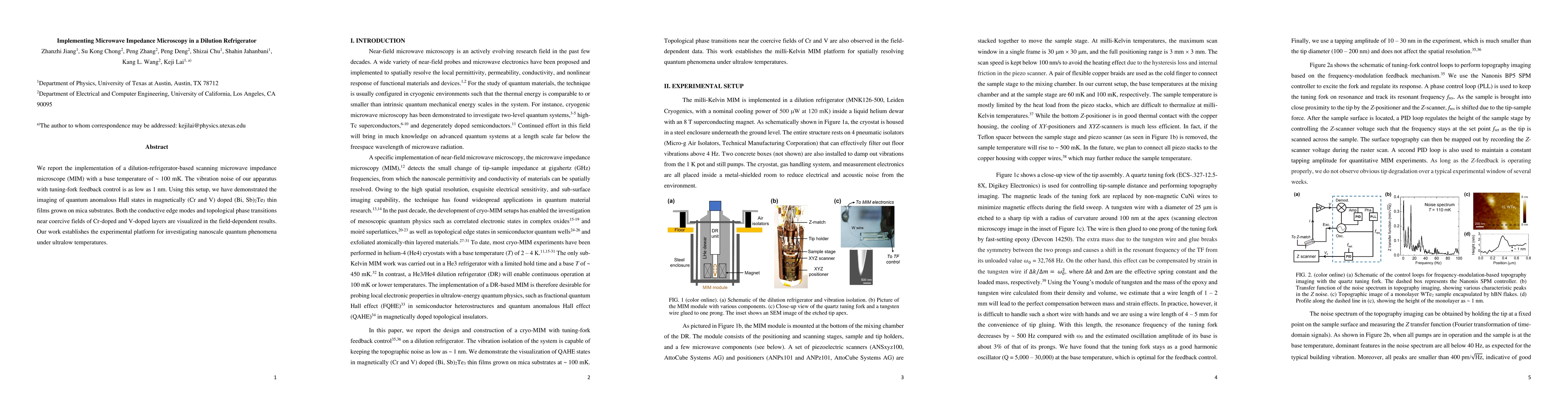
We report the implementation of a dilution-refrigerator-based scanning microwave impedance microscope (MIM) with a base temperature of ~ 100 mK. The vibration noise of our apparatus with tuning-fork...
Implementing microelectromechanical system (MEMS) resonators calls for detailed microscopic understanding of the devices, such as energy dissipation channels, spurious modes, and imperfections from ...
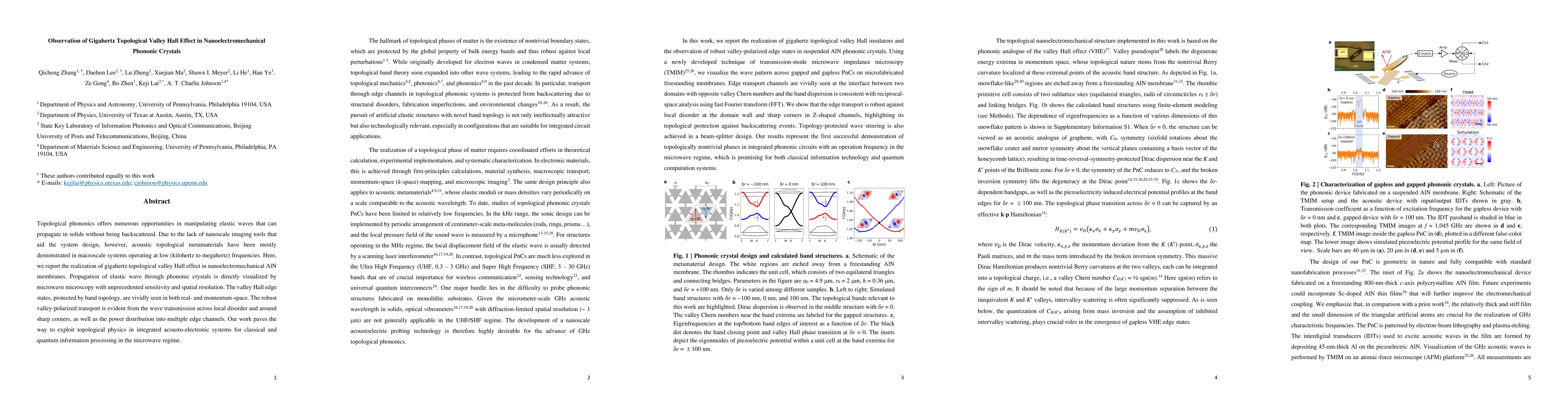
Topological phononics offers numerous opportunities in manipulating elastic waves that can propagate in solids without being backscattered. Due to the lack of nanoscale imaging tools that aid the sy...
In condensed-matter systems, competition between ground states at phase boundaries can lead to significant changes in material properties under external stimuli, particularly when these ground state...
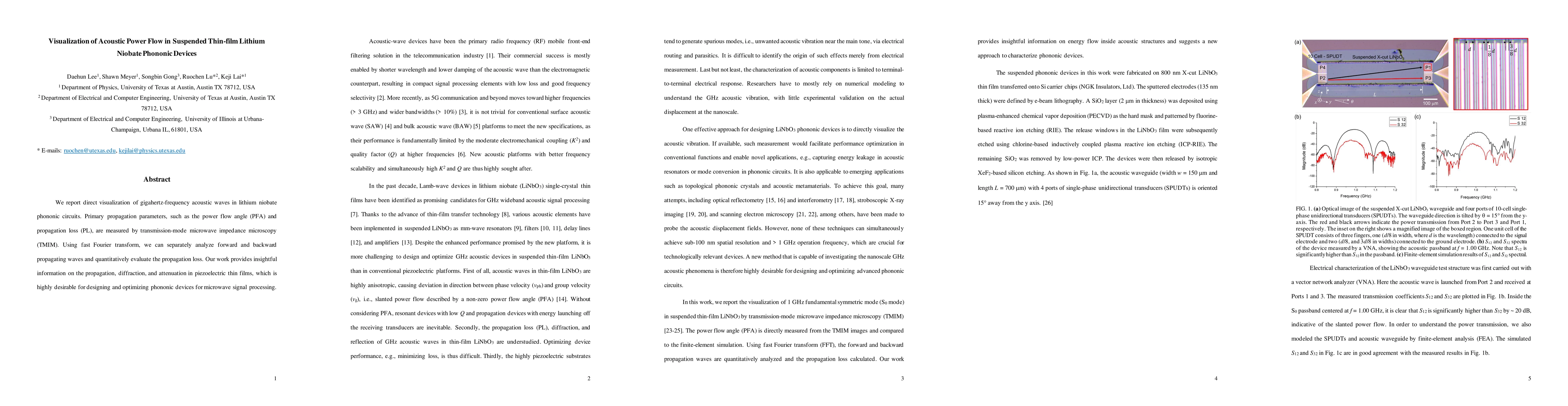
We report direct visualization of gigahertz-frequency acoustic waves in lithium niobate phononic circuits. Primary propagation parameters, such as the power flow angle (PFA) and propagation loss (PL...
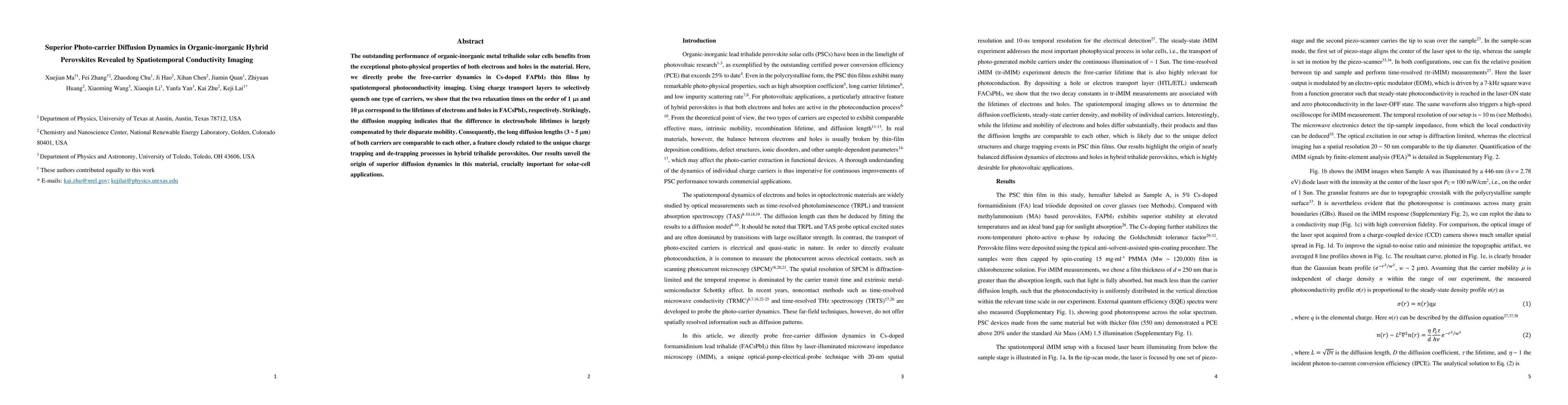
The outstanding performance of organic-inorganic metal trihalide solar cells benefits from the exceptional photo-physical properties of both electrons and holes in the material. Here, we directly pr...
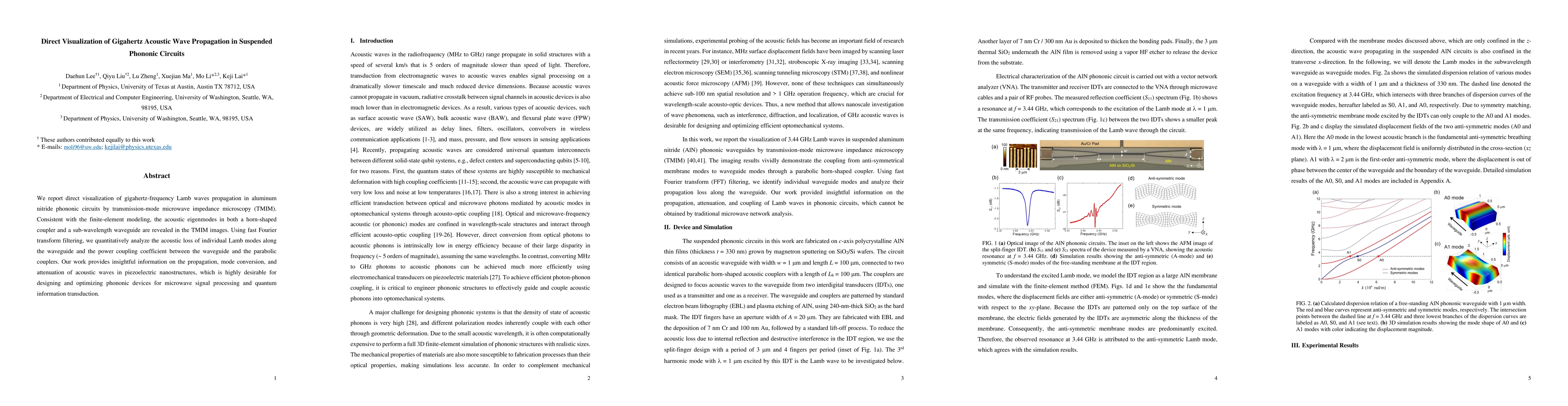
We report direct visualization of gigahertz-frequency Lamb waves propagation in aluminum nitride phononic circuits by transmission-mode microwave impedance microscopy (TMIM). Consistent with the fin...
Monolayer group-V transition metal dichalcogenides in their 1T phase have recently emerged as a platform to investigate rich phases of matter, such as spin liquid and ferromagnetism, resulting from ...
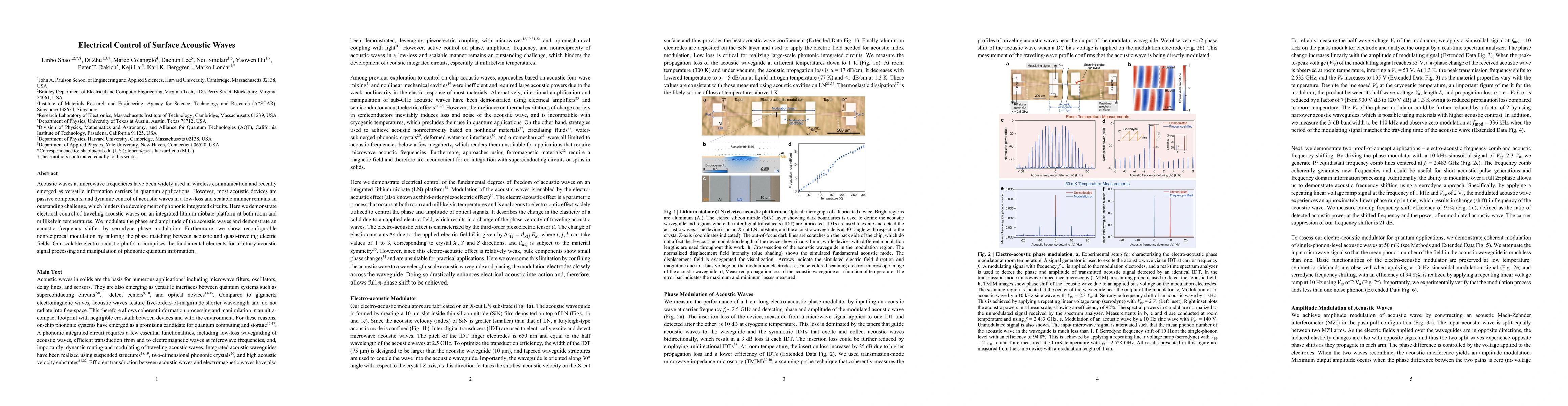
Acoustic waves at microwave frequencies have been widely used in wireless communication and recently emerged as versatile information carriers in quantum applications. However, most acoustic devices...
In moir\'e crystals formed by stacking van der Waals (vdW) materials, surprisingly diverse correlated electronic phases and optical properties can be realized by a subtle change in the twist angle. ...
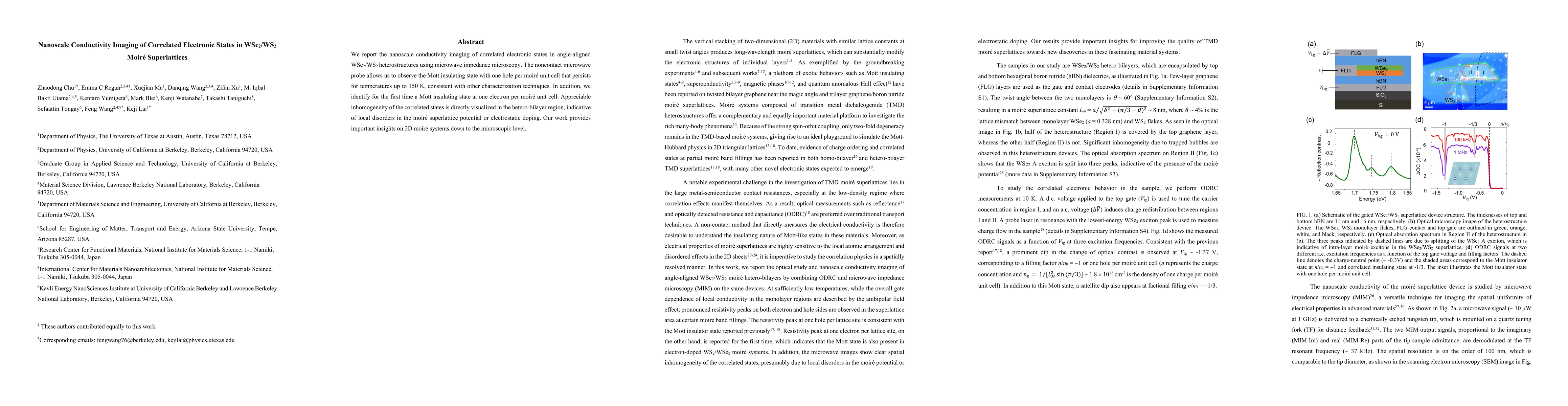
We report the nanoscale conductivity imaging of correlated electronic states in angle-aligned WSe2/WS2 heterostructures using microwave impedance microscopy. The noncontact microwave probe allows us...
The optoelectronic properties of atomically thin transition-metal dichalcogenides are strongly correlated with the presence of defects in the materials, which are not necessarily detrimental for cer...
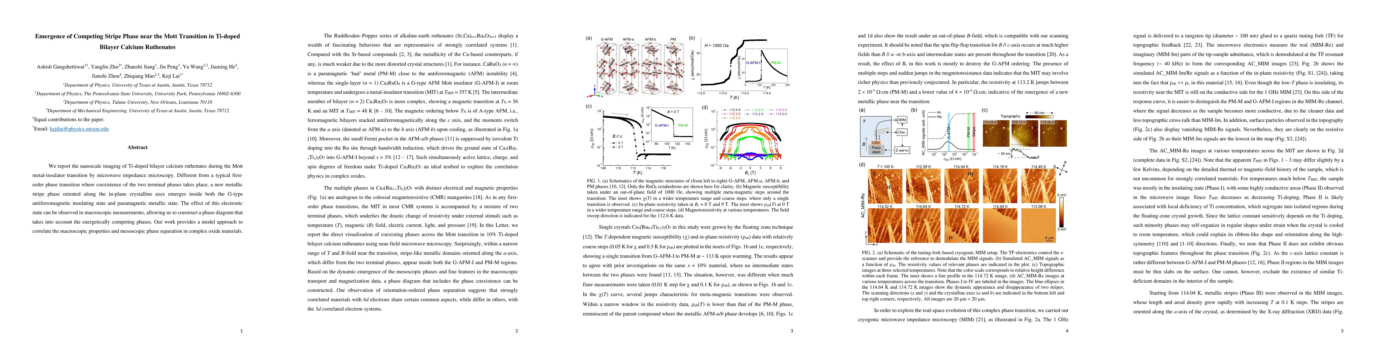
We report the nanoscale imaging of Ti-doped bilayer calcium ruthenates during the Mott metal-insulator transition by microwave impedance microscopy. Different from a typical first-order phase transi...
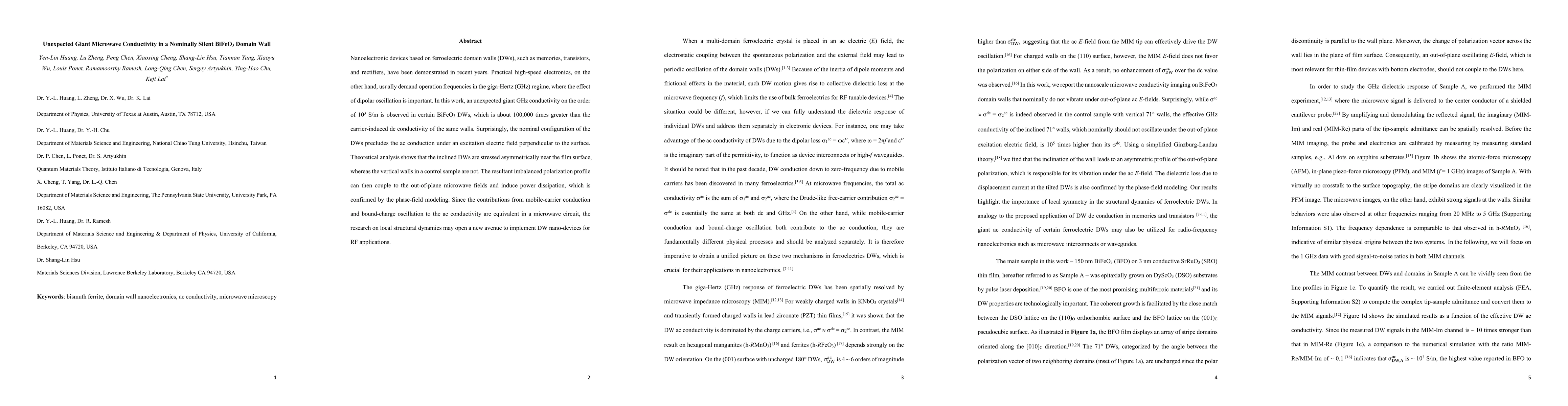
Nanoelectronic devices based on ferroelectric domain walls (DWs), such as memories, transistors, and rectifiers, have been demonstrated in recent years. Practical high-speed electronics, on the othe...
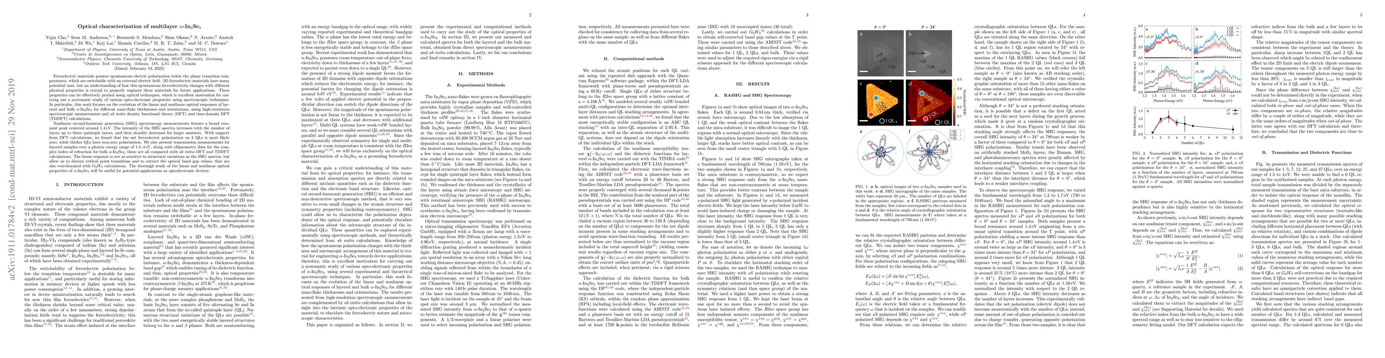
In this work, we report linear and non-linear spectroscopic measurements of chemically-grown layered (from one to 37 quintuple layers) and bulk alpha-In2Se3 samples over a photon energy range of 1.0...
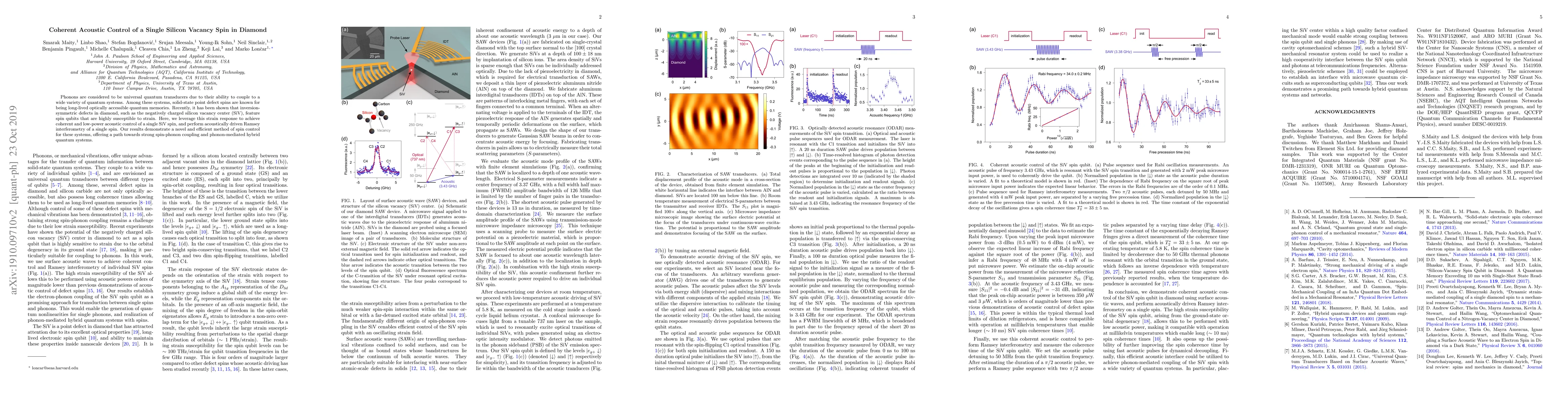
Phonons are considered to be universal quantum transducers due to their ability to couple to a wide variety of quantum systems. Among these systems, solid-state point defect spins are known for bein...
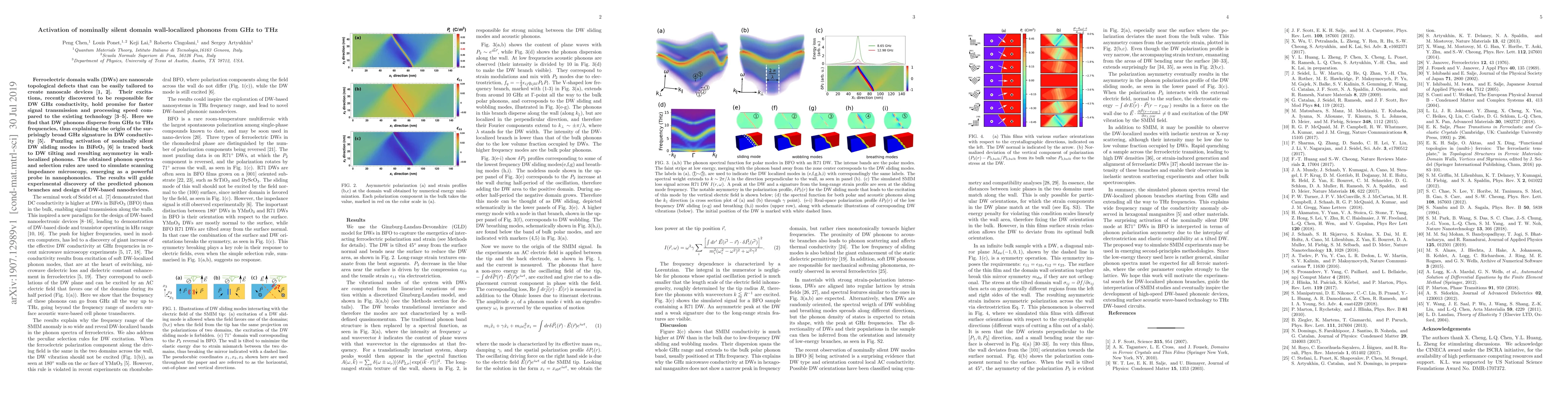
Ferroelectric domain walls (DWs) are nanoscale topological defects that can be easily tailored to create nanoscale devices. Their excitations, recently discovered to be responsible for DW GHz conduc...
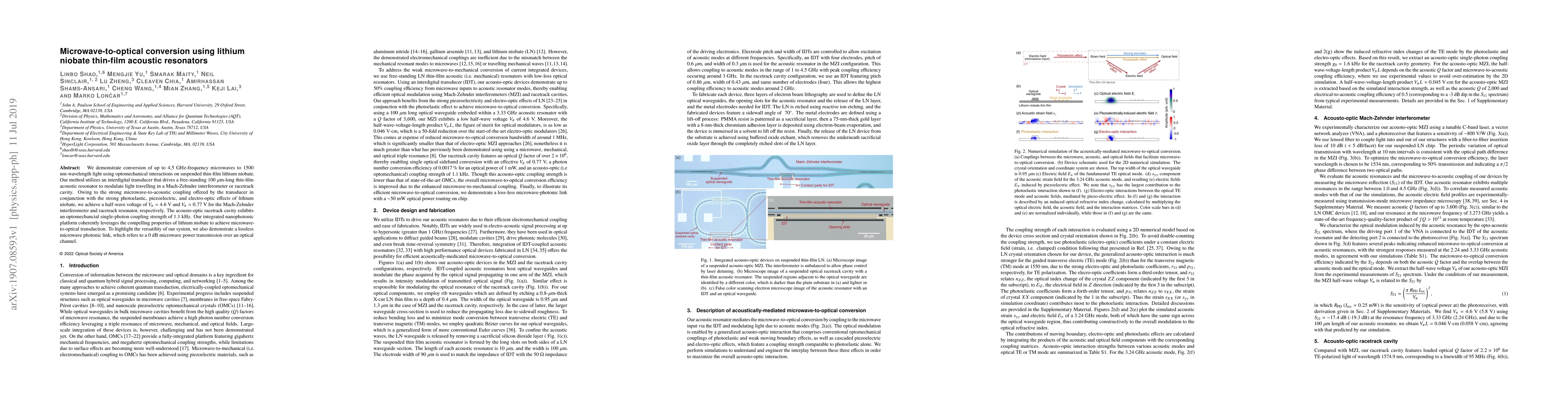
We demonstrate conversion of up to 4.5 GHz-frequency microwaves to 1500 nm-wavelength light using optomechanical interactions on suspended thin-film lithium niobate. Our method utilizes an interdigi...
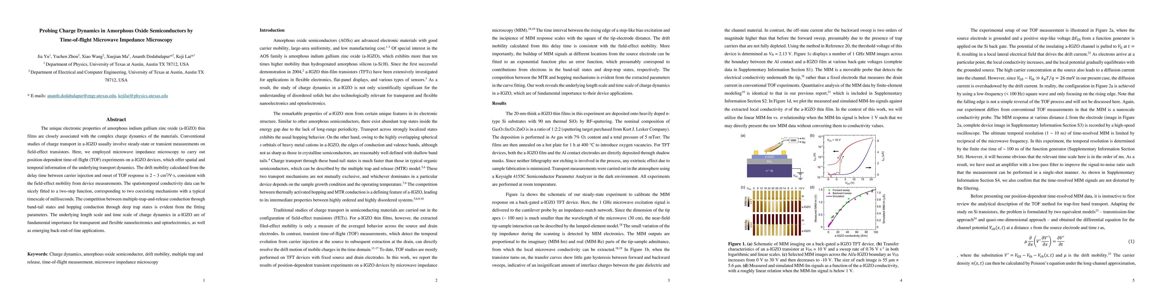
The unique electronic properties of amorphous indium gallium zinc oxide (a-IGZO) thin films are closely associated with the complex charge dynamics of the materials. Conventional studies of charge tra...
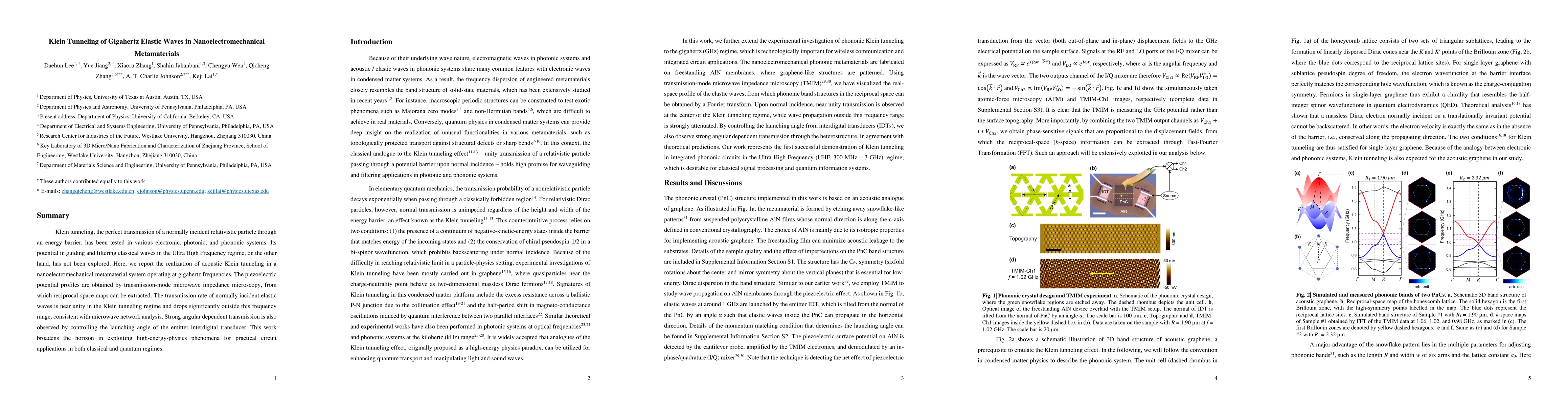
Klein tunneling, the perfect transmission of a normally incident relativistic particle through an energy barrier, has been tested in various electronic, photonic, and phononic systems. Its potential i...
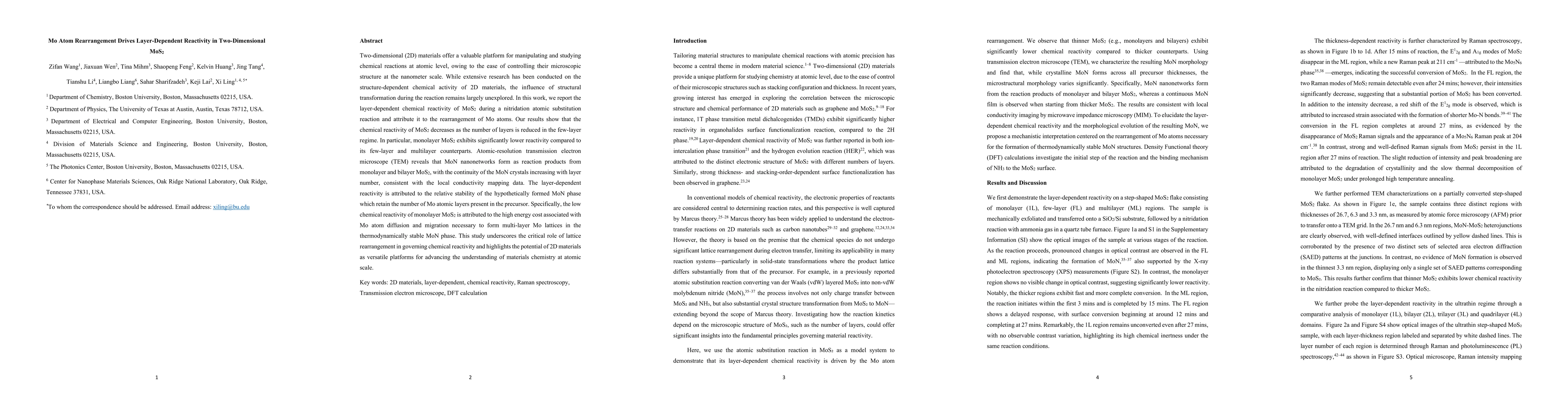
Two-dimensional (2D) materials offer a valuable platform for manipulating and studying chemical reactions at atomic level, owing to the ease of controlling their microscopic structure at the nanometer...
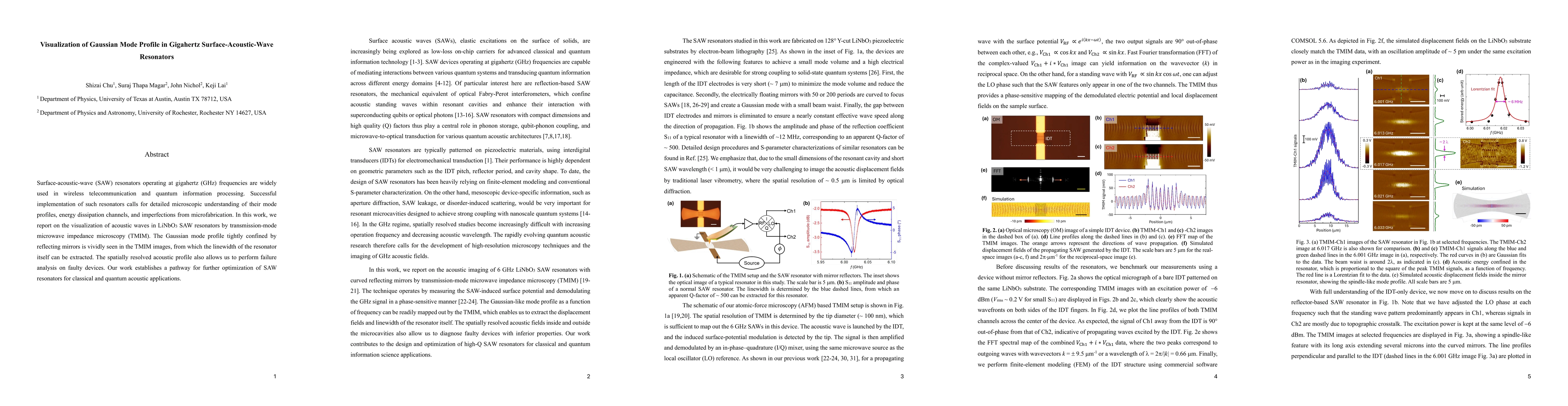
Surface-acoustic-wave (SAW) resonators operating at gigahertz (GHz) frequencies are widely used in wireless telecommunication and quantum information processing. Successful implementation of such reso...
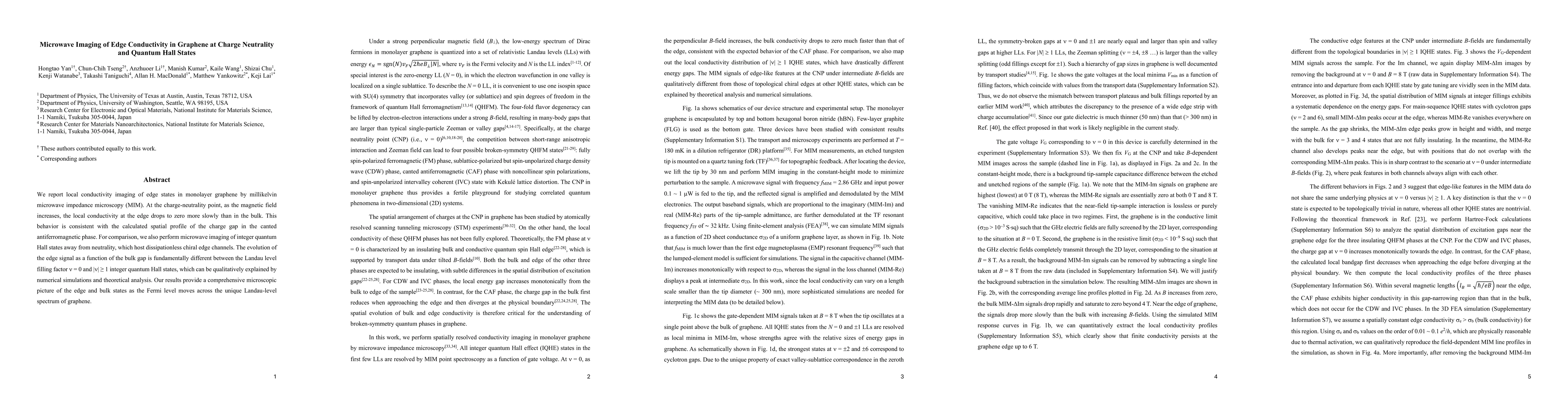
We report local conductivity imaging of edge states in monolayer graphene by millikelvin microwave impedance microscopy (MIM). At the charge-neutrality point, as the magnetic field increases, the loca...