Academic Profile
Statistics
Similar Authors
Papers on arXiv
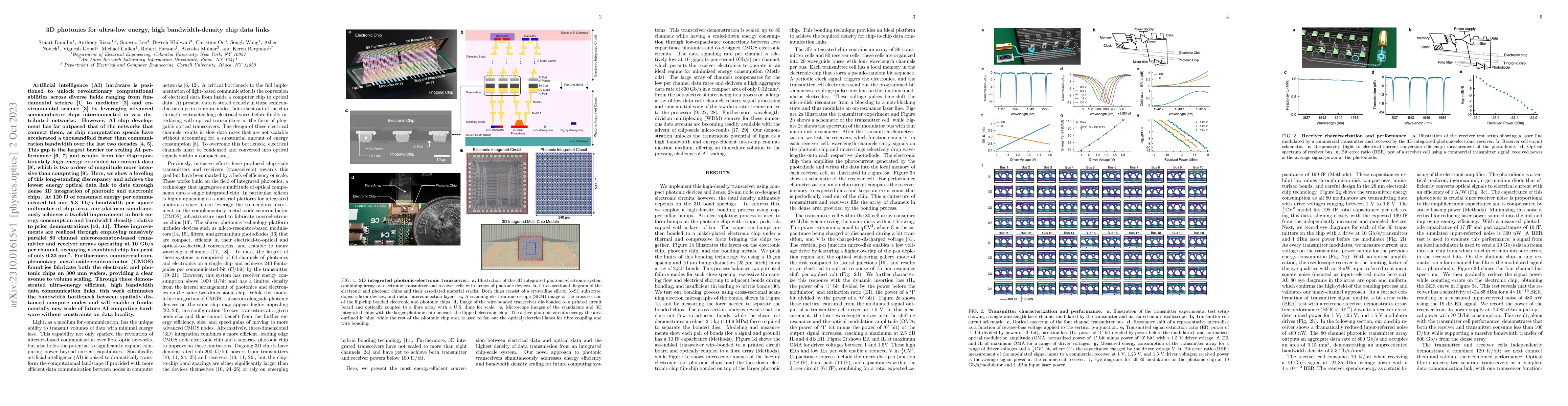
Artificial intelligence (AI) hardware is positioned to unlock revolutionary computational abilities across diverse fields ranging from fundamental science [1] to medicine [2] and environmental scien...
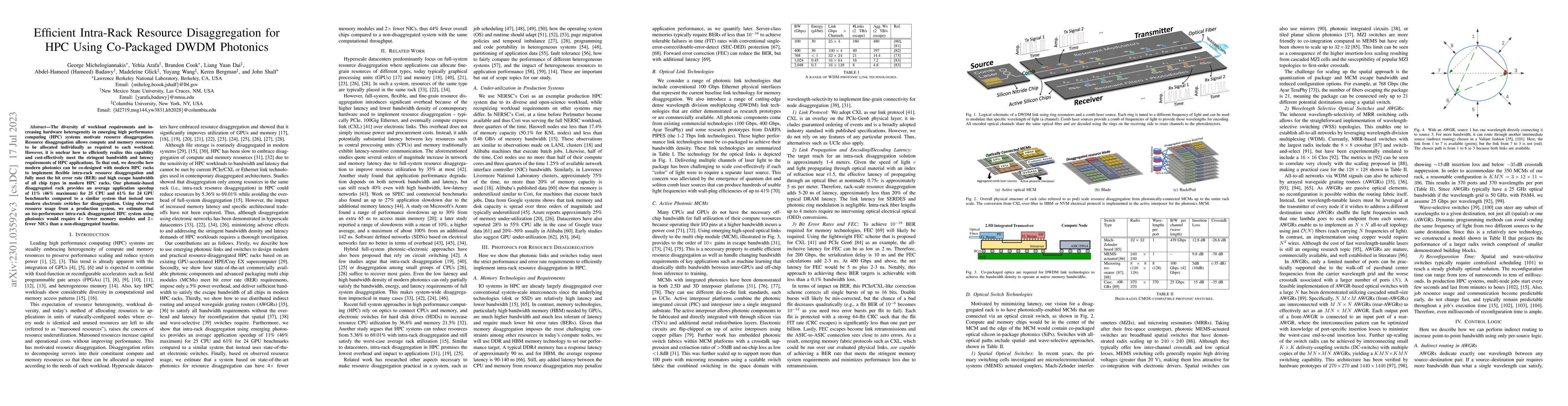
The diversity of workload requirements and increasing hardware heterogeneity in emerging high performance computing (HPC) systems motivate resource disaggregation. Resource disaggregation allows com...
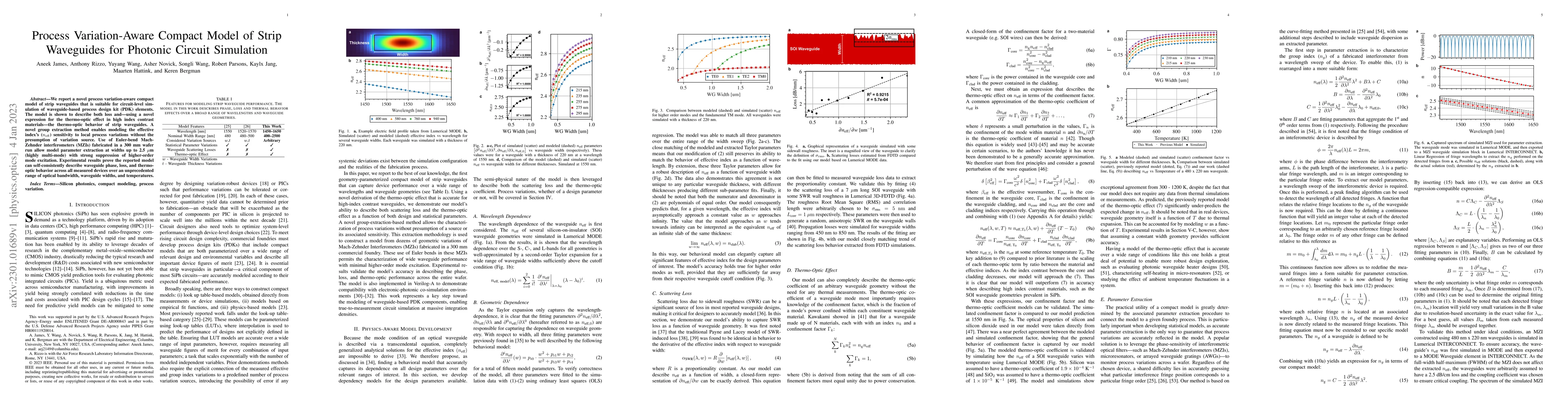
We report a novel process variation-aware compact model of strip waveguides that is suitable for circuit-level simulation of waveguide-based process design kit (PDK) elements. The model is shown to ...
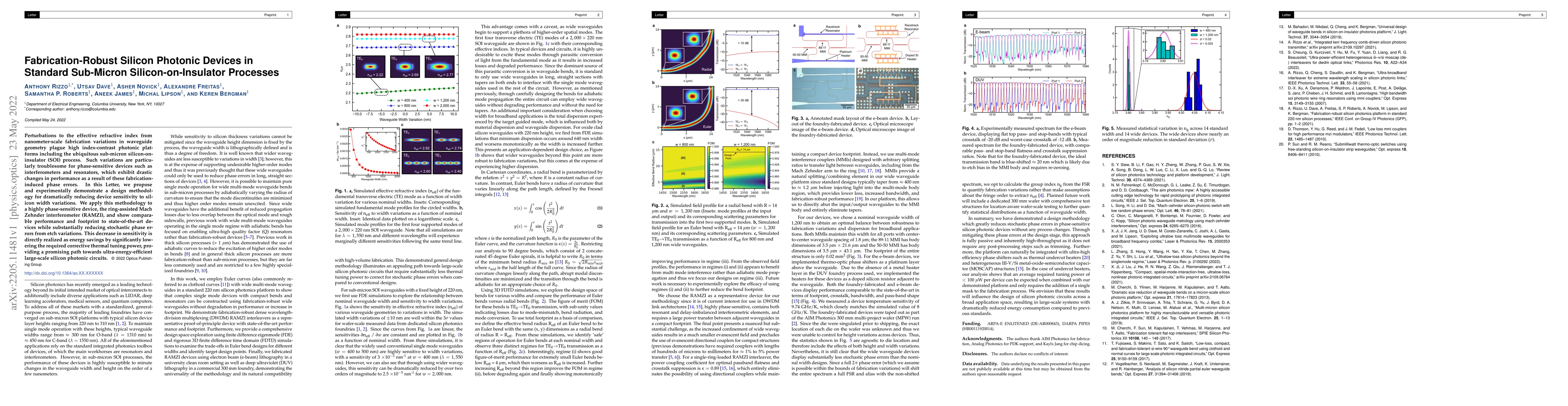
Perturbations to the effective refractive index from nanometer-scale fabrication variations in waveguide geometry plague high index-contrast photonic platforms including the ubiquitous sub-micron si...
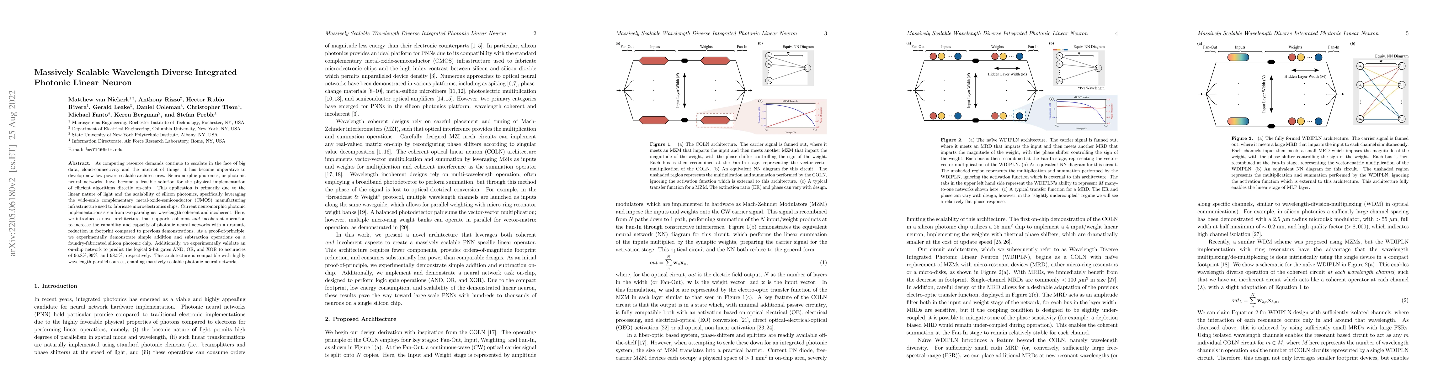
As computing resource demands continue to escalate in the face of big data, cloud-connectivity and the internet of things, it has become imperative to develop new low-power, scalable architectures. ...
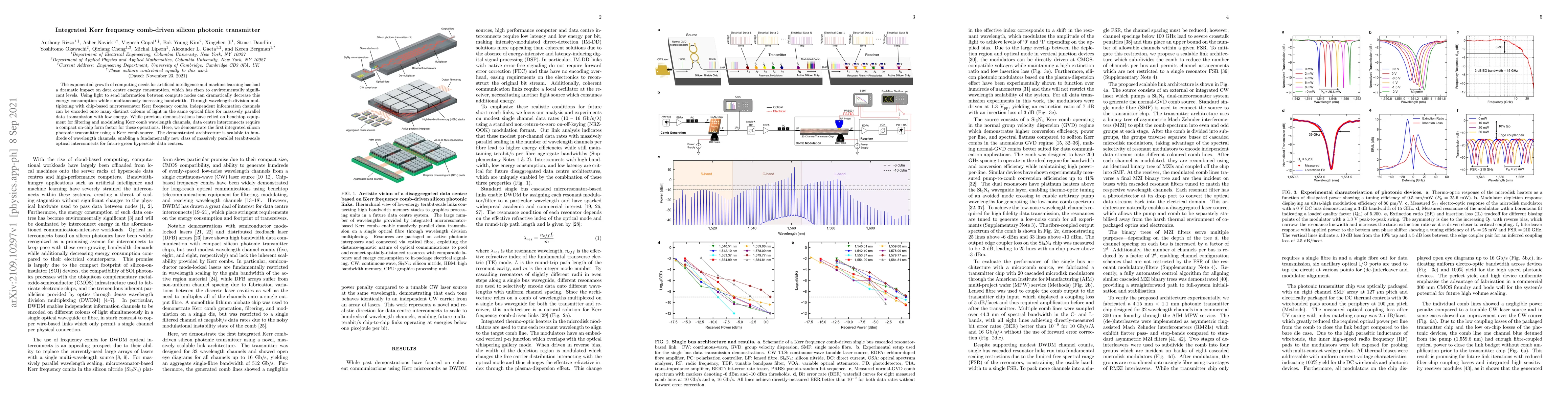
The exponential growth of computing needs for artificial intelligence and machine learning has had a dramatic impact on data centre energy consumption, which has risen to environmentally significant...
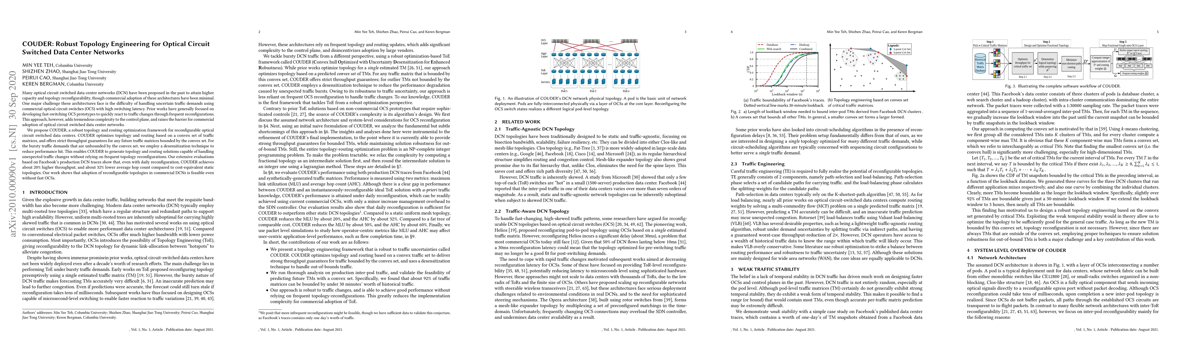
Many optical circuit switched data center networks (DCN) have been proposed in the past to attain higher capacity and topology reconfigurability, though commercial adoption of these architectures ha...
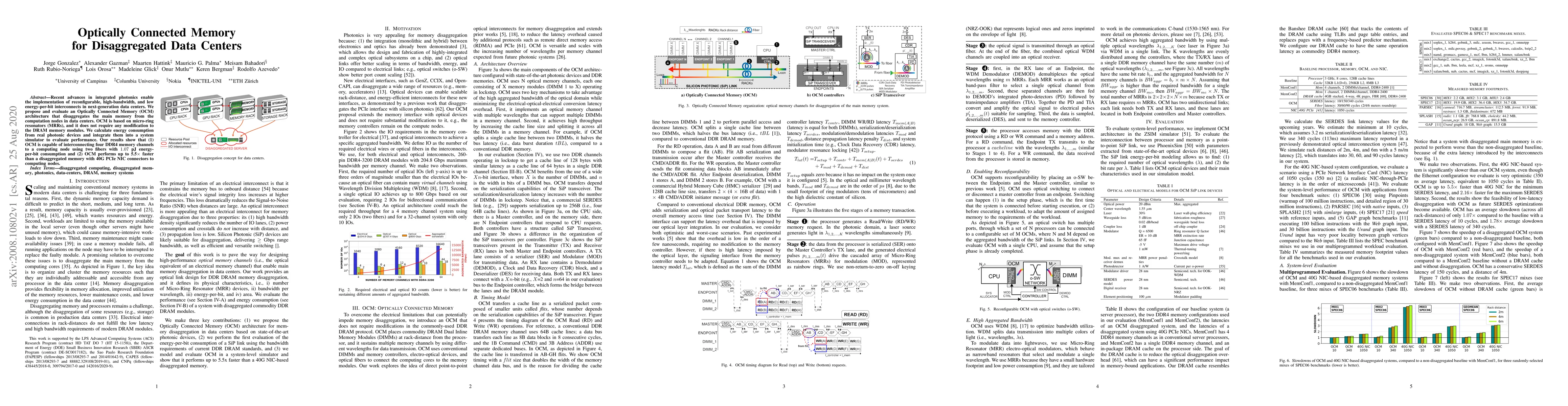
Recent advances in integrated photonics enable the implementation of reconfigurable, high-bandwidth, and low energy-per-bit interconnects in next-generation data centers. We propose and evaluate an ...
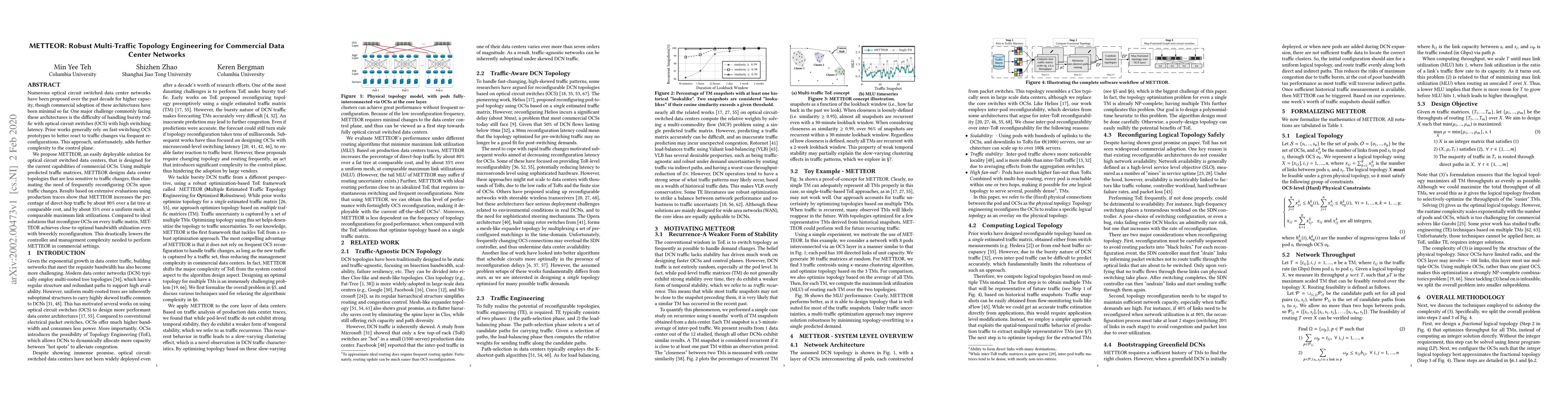
Numerous optical circuit switched data center networks have been proposed over the past decade for higher capacity, though commercial adoption of these architectures have been minimal so far. One ma...
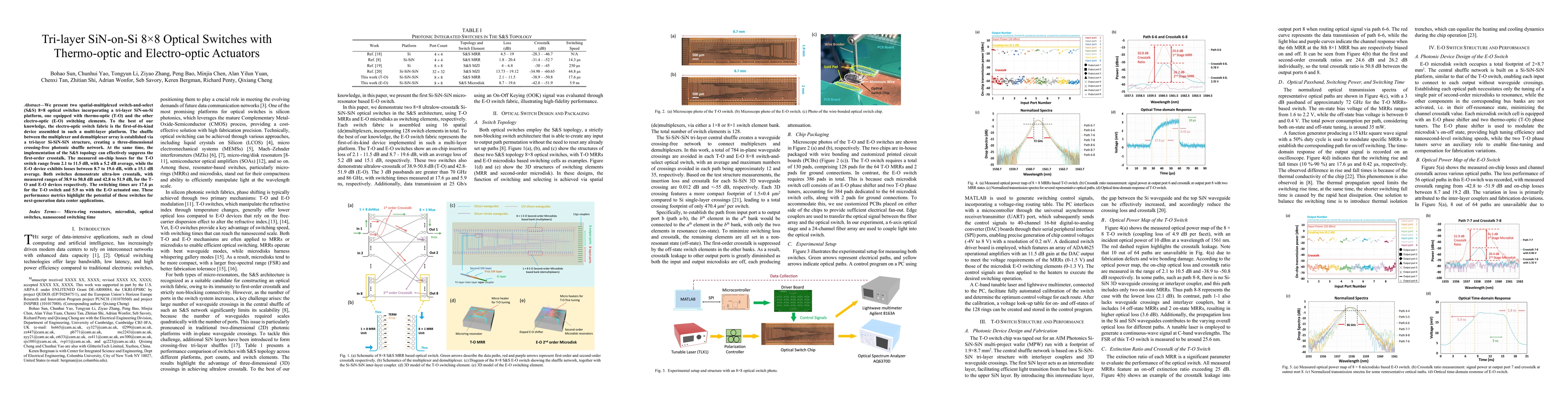
We present two spatial-multiplexed switch-and-select (S&S) 8x8 optical switches incorporating a tri-layer SiN-on-Si platform, one equipped with thermo-optic (T-O) and the other electro-optic (E-O) swi...
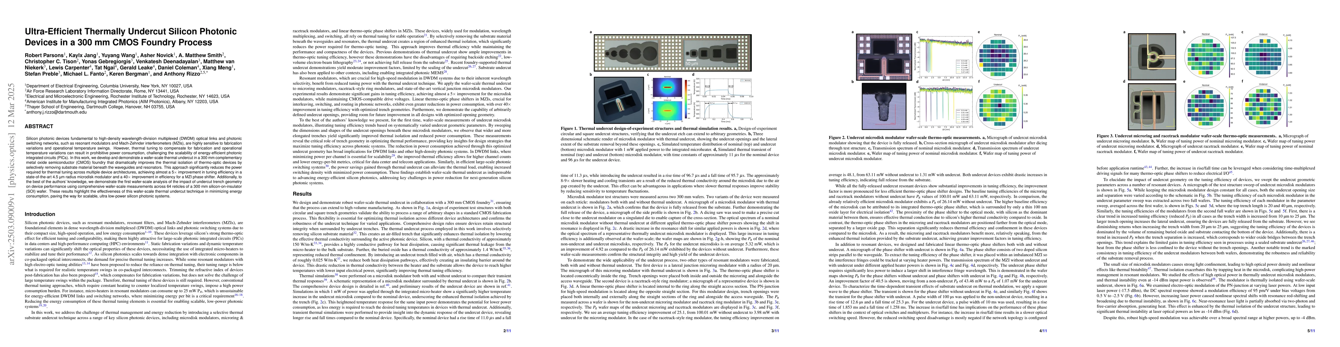
Silicon photonic devices fundamental to high-density wavelength-division multiplexed (DWDM) optical links and photonic switching networks, such as resonant modulators and Mach-Zehnder interferometers ...