Academic Profile
Statistics
Similar Authors
Papers on arXiv
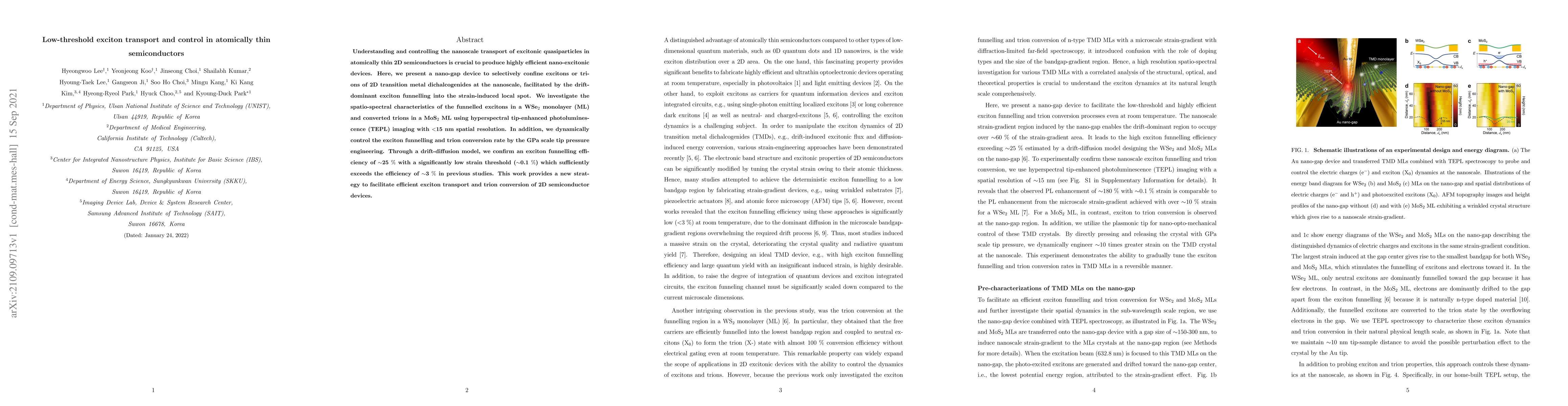
Understanding and controlling the nanoscale transport of excitonic quasiparticles in atomically thin 2D semiconductors is crucial to produce highly efficient nano-excitonic devices. Here, we present...
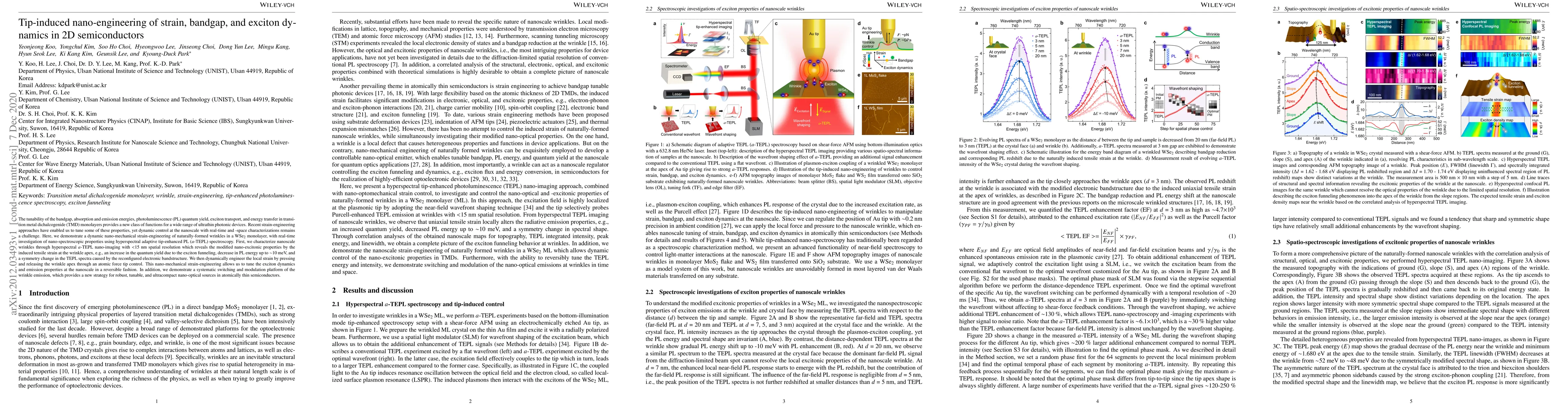
The tunability of the bandgap, absorption and emission energies, photoluminescence (PL) quantum yield, exciton transport, and energy transfer in transition metal dichalcogenide (TMD) monolayers prov...
Among transition metal dichalcogenides (TMdCs) as alternatives for Pt-based catalysts, metallic-TMdCs catalysts have highly reactive basal-plane but are unstable. Meanwhile, chemically stable semico...
Growth of two-dimensional van der Waals layered single-crystal (SC) films is highly desired to manifest intrinsic material sciences and unprecedented devices for industrial applications. While wafer...
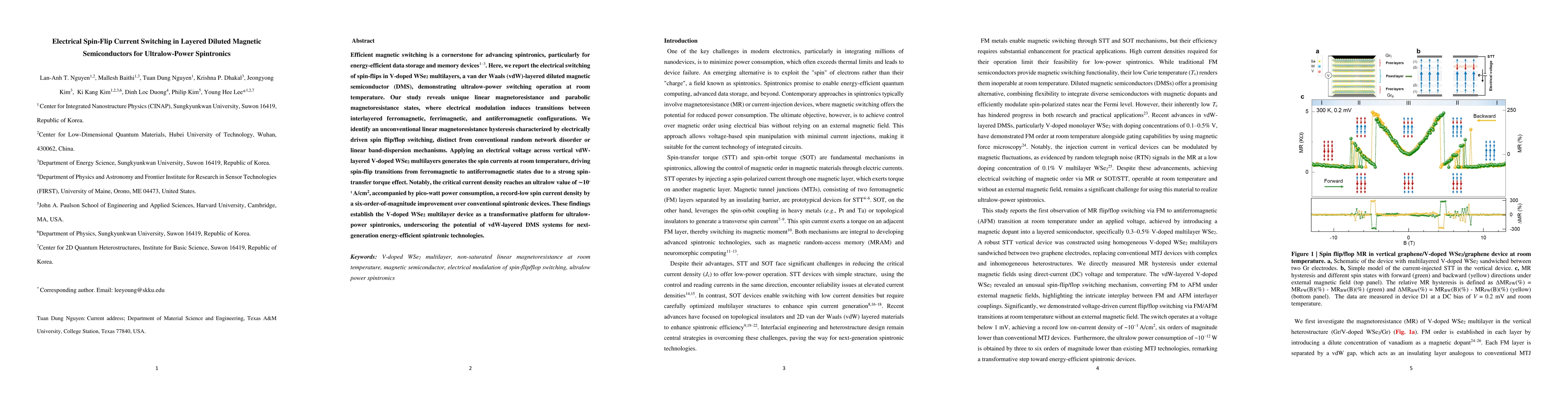
Efficient magnetic switching is a cornerstone for advancing spintronics, particularly for energy-efficient data storage and memory devices. Here, we report the electrical switching of spin-flips in V-...
Over the past two decades, 2D materials have rapidly evolved into a diverse and expanding family of material platforms. Many members of this materials class have demonstrated their potential to delive...
Hexagonal boron nitride (hBN) supports a wide range of two-dimensional (2D) technologies, yet assessing its crystalline quality over large areas remains a fundamental challenge. Both antiparallel doma...
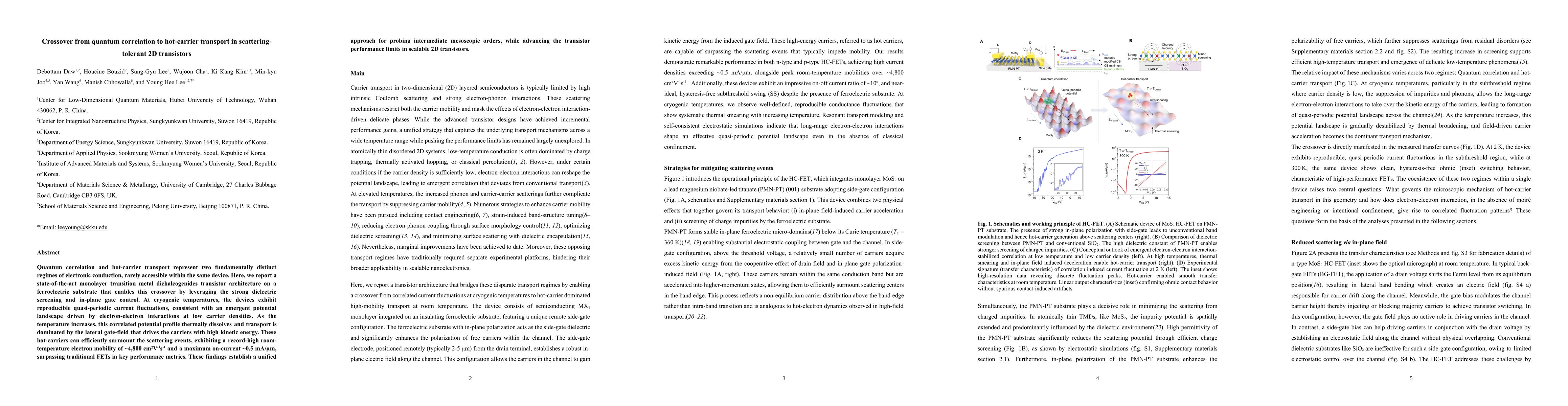
Quantum correlation and hot-carrier transport represent two fundamentally distinct regimes of electronic conduction, rarely accessible within the same device. Here, we report a state-of-the-art monola...
Hybrid heterostructures composed of graphene and perovskite oxides provide a promising platform for exploiting synergetic interfacial functionalities. Conventional fabrication methods of the hybrid he...