Academic Profile
Statistics
Similar Authors
Papers on arXiv
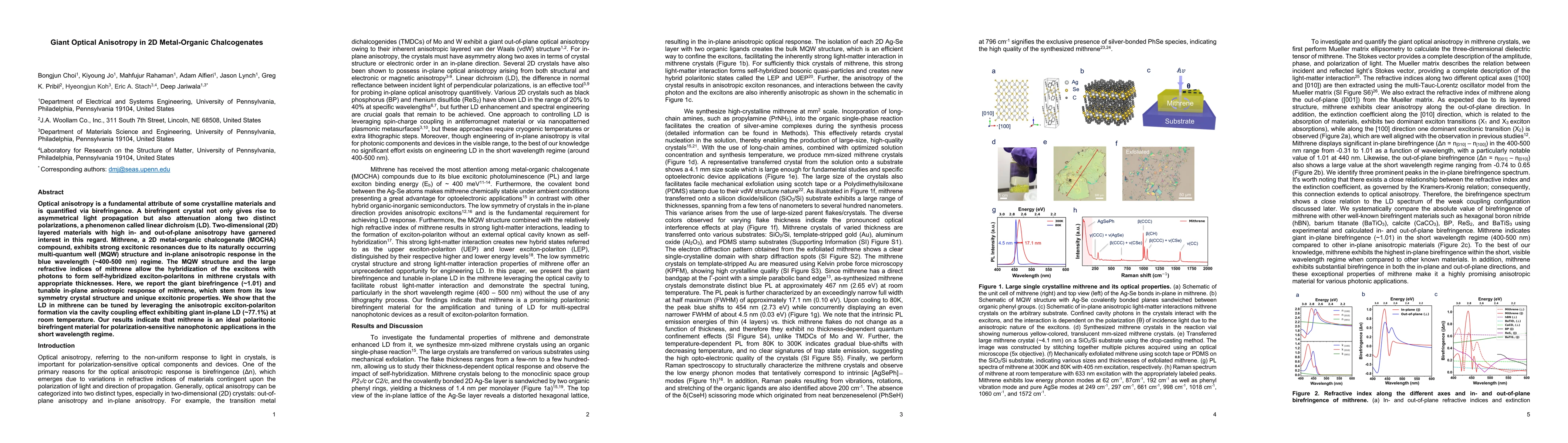
Optical anisotropy is a fundamental attribute of some crystalline materials and is quantified via birefringence. A birefringent crystal not only gives rise to asymmetrical light propagation but also...
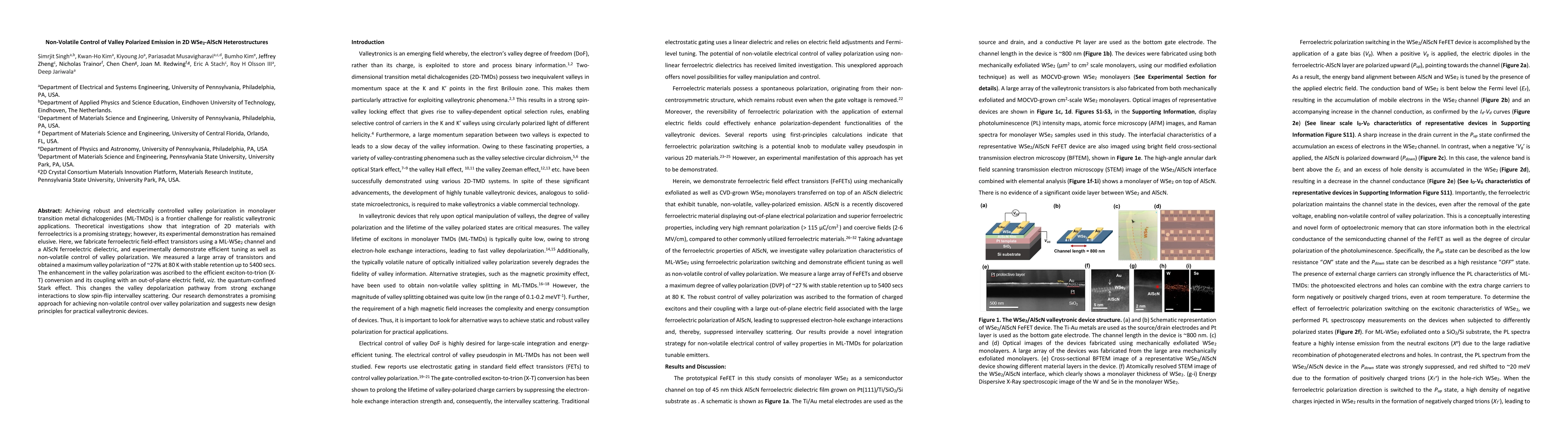
Achieving robust and electrically controlled valley polarization in monolayer transition metal dichalcogenides (ML-TMDs) is a frontier challenge for realistic valleytronic applications. Theoretical ...
Two-dimensional (2D) semiconductors are promising candidates for optoelectronic application and quantum information processes due to their inherent out-of-plane 2D confinement. In addition, they off...
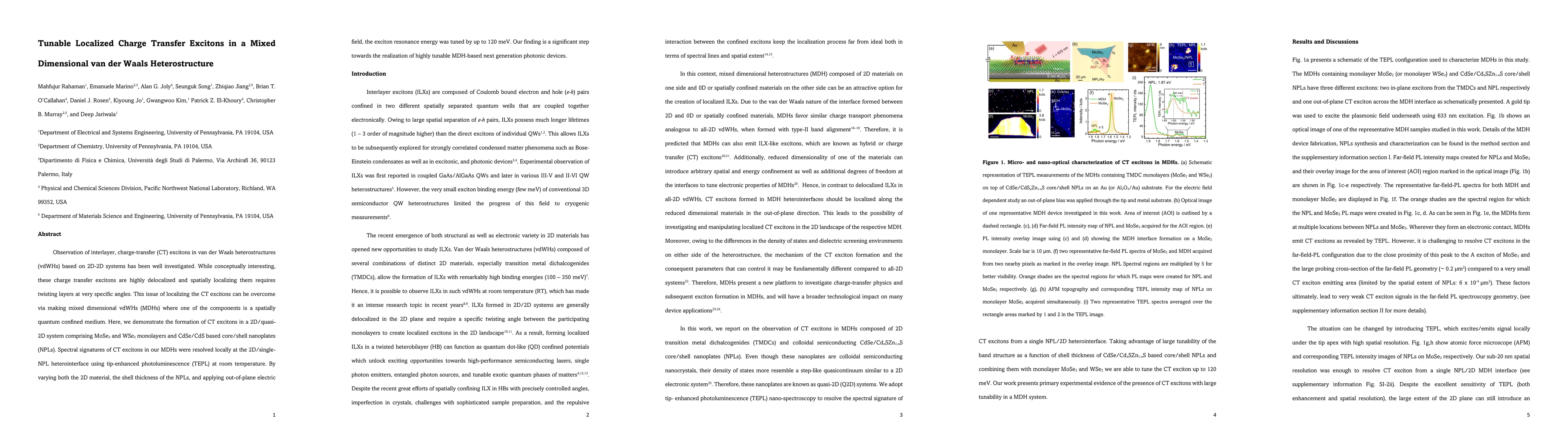
Observation of interlayer, charge-transfer (CT) excitons in van der Waals heterostructures (vdWHs) based on 2D-2D systems has been well investigated. While conceptually interesting, these charge tra...
Strong light-matter interactions in localized nano-emitters when placed near metallic mirrors have been widely reported via spectroscopic studies in the optical far-field. Here, we report a near-fie...
Two-dimensional chalcogenide semiconductors have recently emerged as a host material for quantum emitters of single photons. While several reports on defect and strain-induced single photon emission...
Light-matter coupling in excitonic materials has been the subject of intense investigation due to emergence of new excitonic materials. Two-dimensional layered hybrid organic/inorganic perovskites (...
Van der Waals materials exhibit naturally passivated surfaces and can form versatile heterostructures, enabling observation of carrier transport mechanisms not seen in three-dimensional materials. H...
Semiconductors in all dimensionalities ranging from 0D quantum dots and molecules to 3D bulk crystals support bound electron-hole pair quasiparticles termed as excitons. Over the past two decades, t...
The semiconductor-metal junction is one of the most critical factors for high performance electronic devices. In two-dimensional (2D) semiconductor devices, minimizing the voltage drop at this junct...
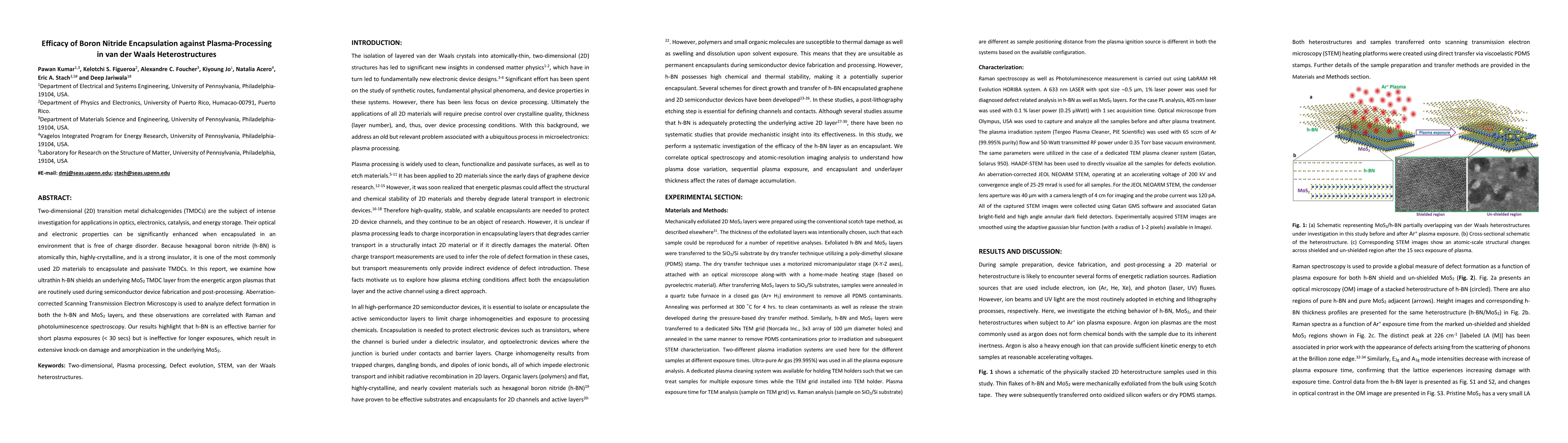
Two-dimensional (2D) transition metal dichalcogenides (TMDCs) are the subject of intense investigation for applications in optics, electronics, catalysis, and energy storage. Their optical and elect...
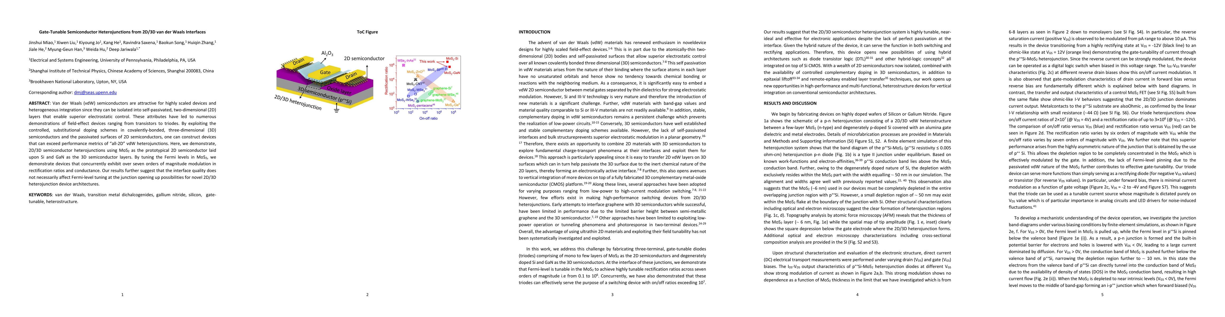
Van der Waals (vdW) semiconductors are attractive for highly scaled devices and heterogeneous integration since they can be isolated into self-passivated, two-dimensional (2D) layers that enable sup...
Van der Waals materials and heterostructures manifesting strongly bound room temperature exciton states exhibit emergent physical phenomena and are of a great promise for optoelectronic applications...