Academic Profile
Statistics
Similar Authors
Papers on arXiv
A one-dimensional (1D) model has been constructed to study the transition of the time-dependent ultrafast laser photo-electron emission from a flat metallic surface to the space charge limited (SCL)...
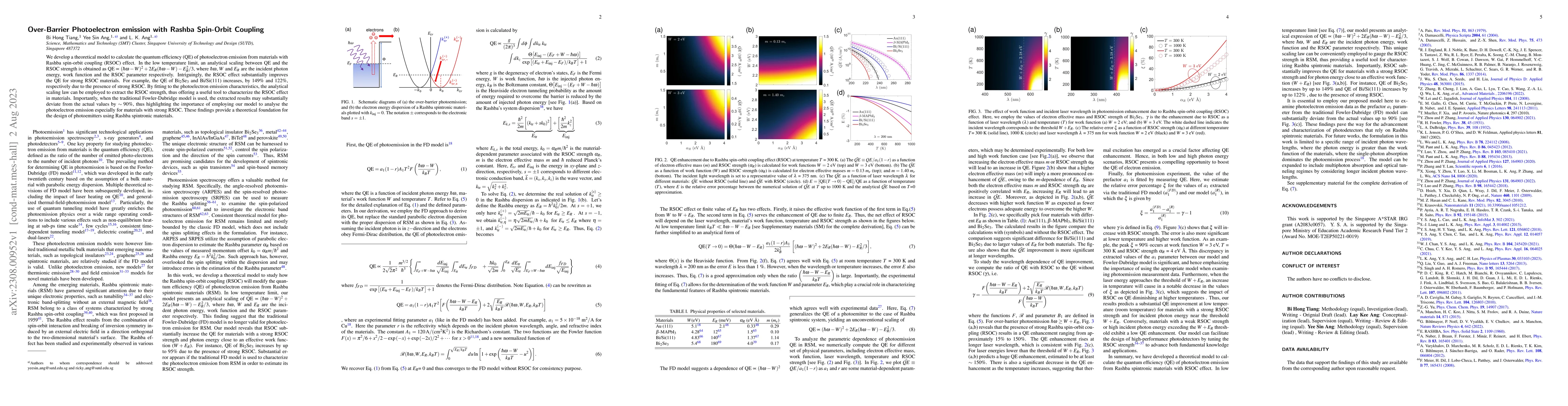
We develop a theoretical model to calculate the quantum efficiency (QE) of photoelectron emission from materials with Rashba spin-orbit coupling (RSOC) effect. In the low temperature limit, an analy...
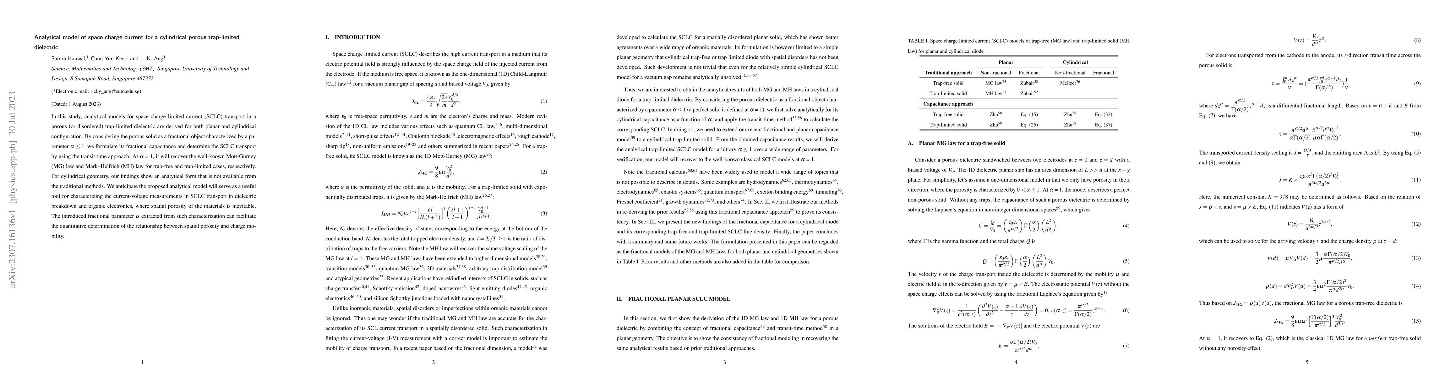
In this study, analytical models for space charge limited current (SCLC) transport in a porous (or disordered) trap-limited dielectric are derived for both planar and cylindrical configuration. By c...
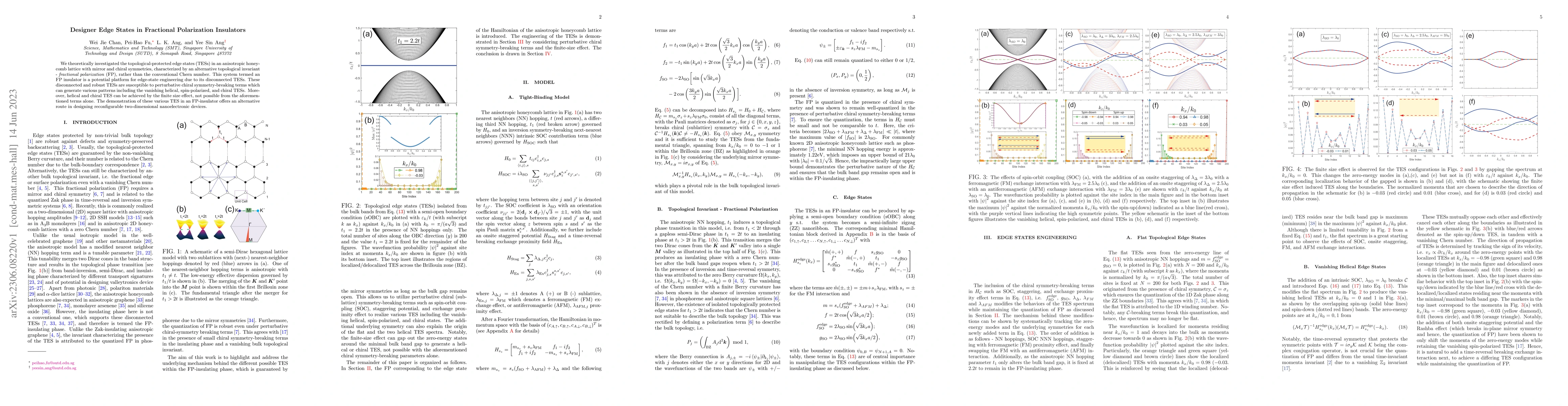
We theoretically investigated the topological-protected edge states (TESs) in an anisotropic honeycomb lattice with mirror and chiral symmetries, characterized by an alternative topological invarian...
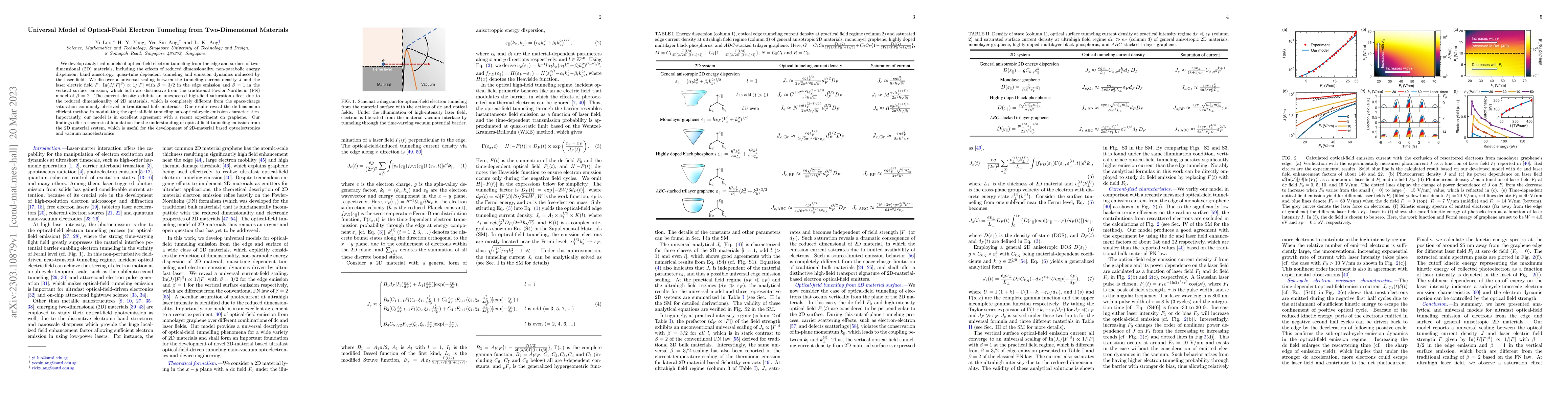
We develop analytical models of optical-field electron tunneling from the edge and surface of two-dimensional (2D) materials, including the effects of reduced dimensionality, non-parabolic energy di...
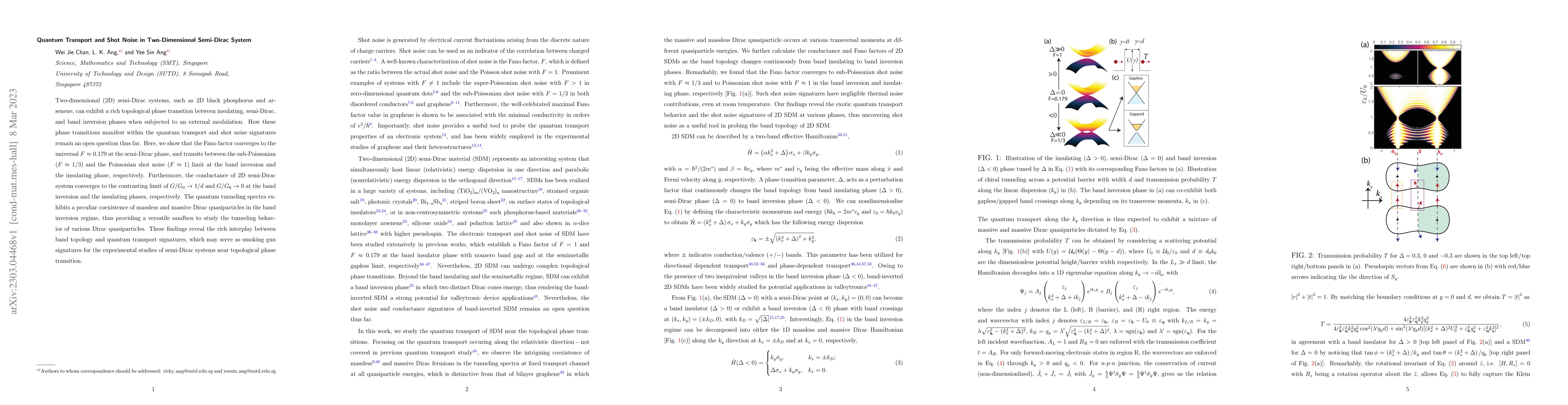
Two-dimensional ($2$D) semi-Dirac systems, such as $2$D black phosphorus and arsenene, can exhibit a rich topological phase transition between insulating, semi-Dirac, and band inversion phases when ...
Realizing both ultra-low breakdown voltage and ultra-high gain has been one of the major challenges in the development of high-performance avalanche photodetector. Here, we report that an ultra-high...
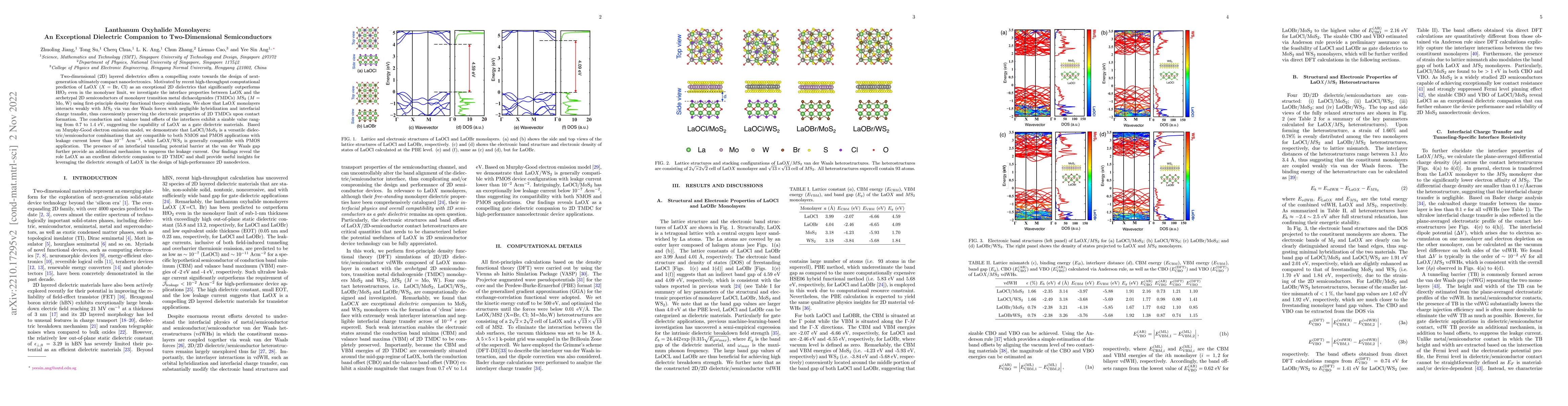
Two-dimensional (2D) layered dielectrics offers a compelling route towards the design of next-generation ultimately compact nanoelectronics. Motivated by recent high-throughput computational predict...
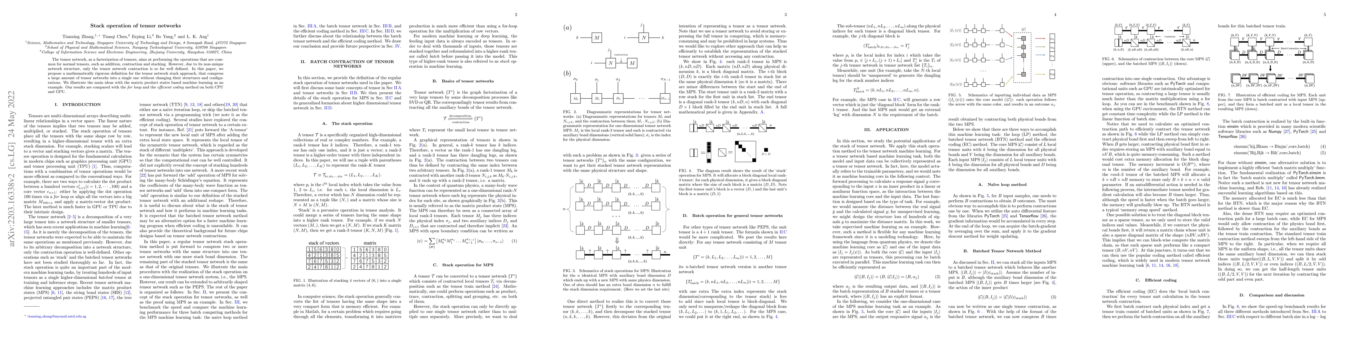
The tensor network, as a facterization of tensors, aims at performing the operations that are common for normal tensors, such as addition, contraction and stacking. However, due to its non-unique ne...
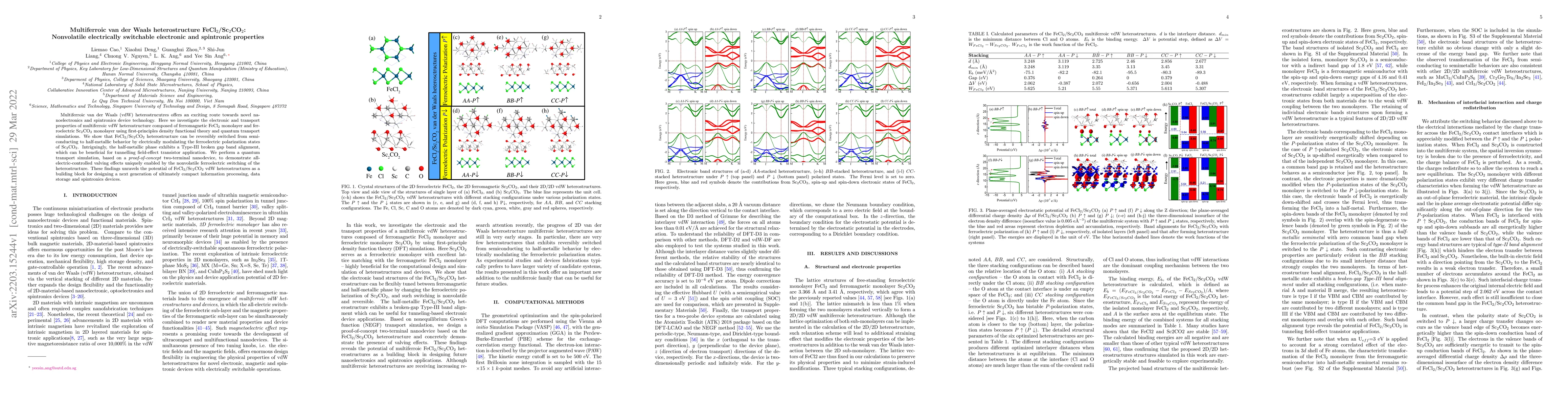
Multiferroic van der Waals (vdW) heterostrucutres offers an exciting route towards novel nanoelectronics and spintronics device technology. Here we investigate the electronic and transport propertie...
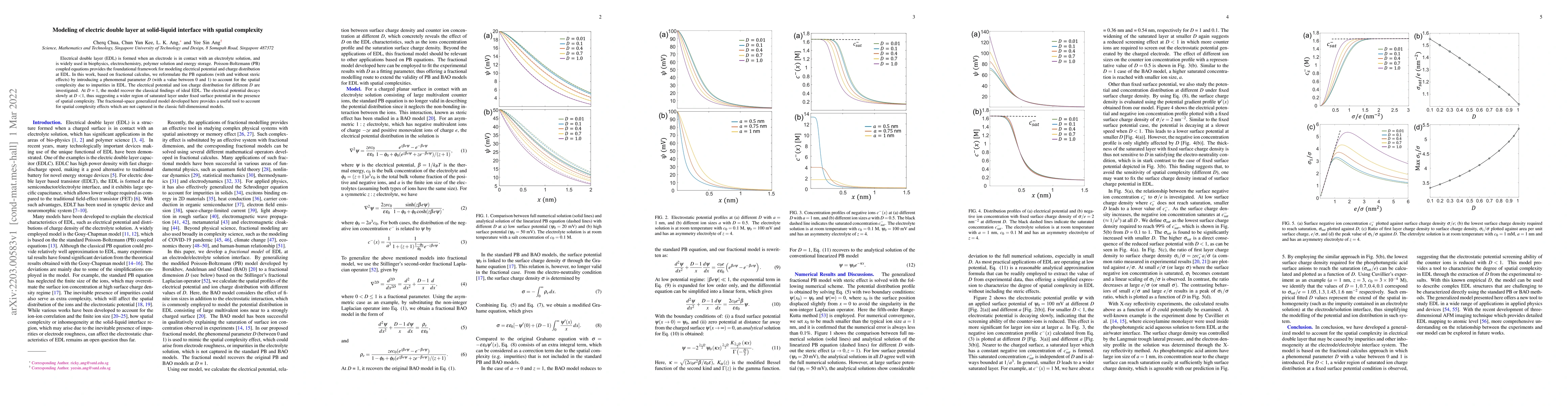
Electrical double layer (EDL) is formed when an electrode is in contact with an electrolyte solution, and is widely used in biophysics, electrochemistry, polymer solution and energy storage. Poisson...
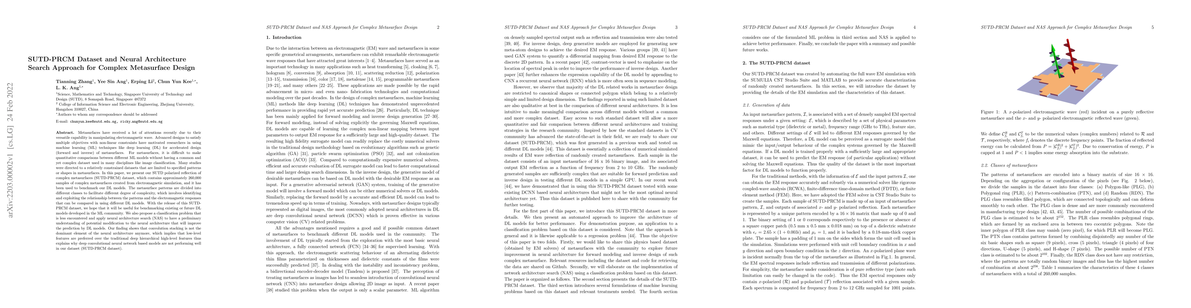
Metasurfaces have received a lot of attentions recently due to their versatile capability in manipulating electromagnetic wave. Advanced designs to satisfy multiple objectives with non-linear constr...
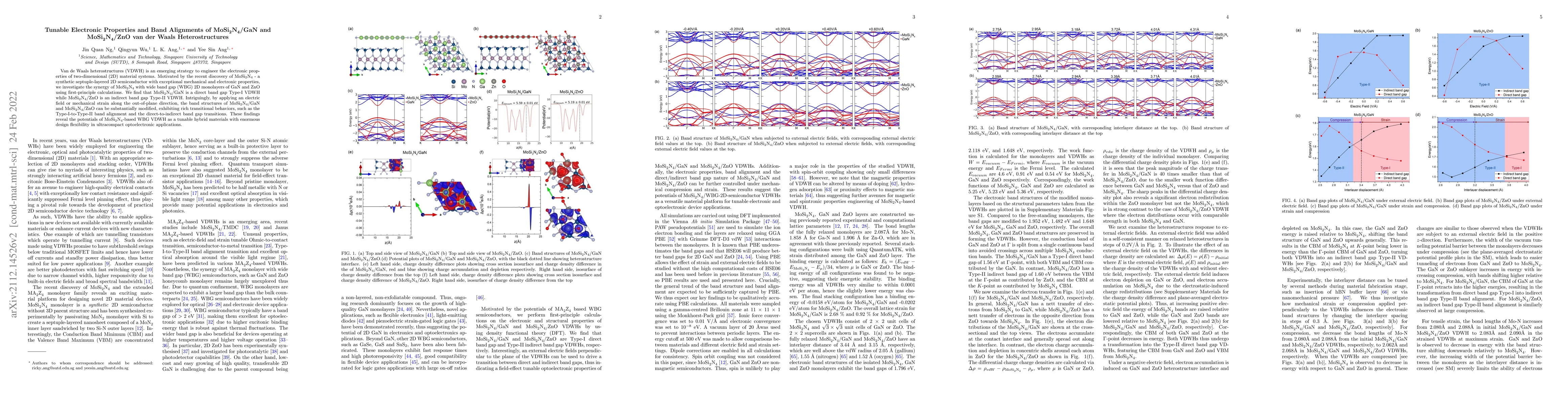
Van de Waals heterostructures (VDWH) is an emerging strategy to engineer the electronic properties of two-dimensional (2D) material systems. Motivated by the recent discovery of MoSi$_2$N$_4$ - a sy...
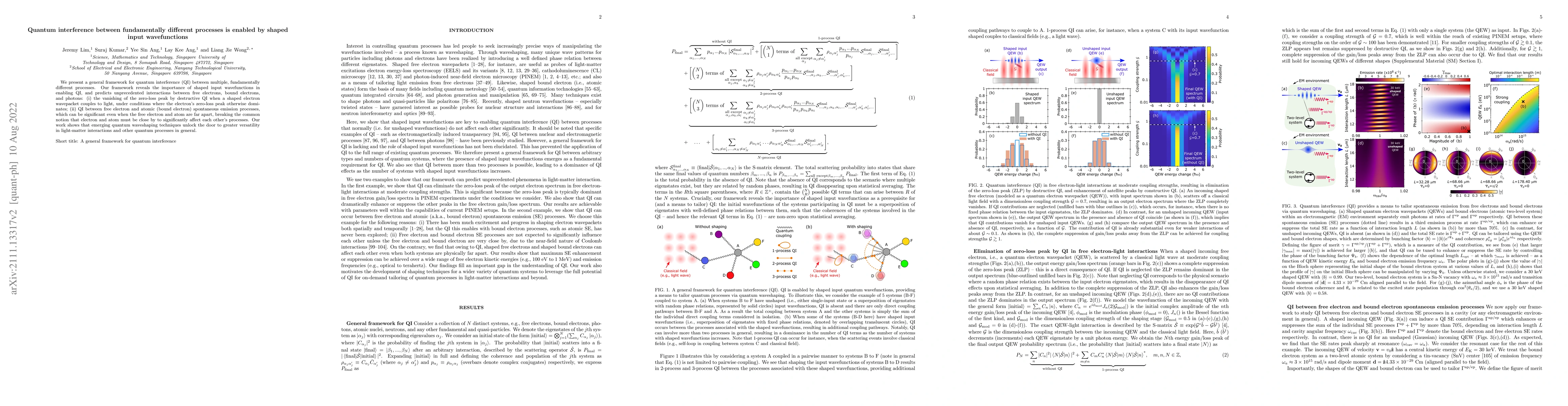
We present a general framework for quantum interference (QI) between multiple, fundamentally different processes. Our framework reveals the importance of shaped input wavefunctions in enabling QI, a...
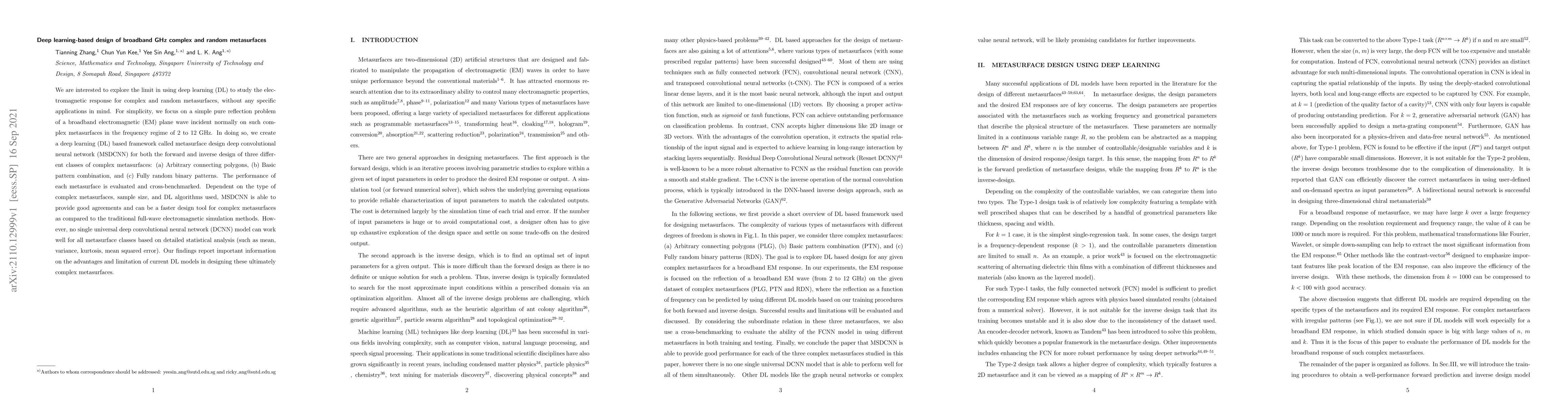
We are interested to explore the limit in using deep learning (DL) to study the electromagnetic response for complex and random metasurfaces, without any specific applications in mind. For simplicit...
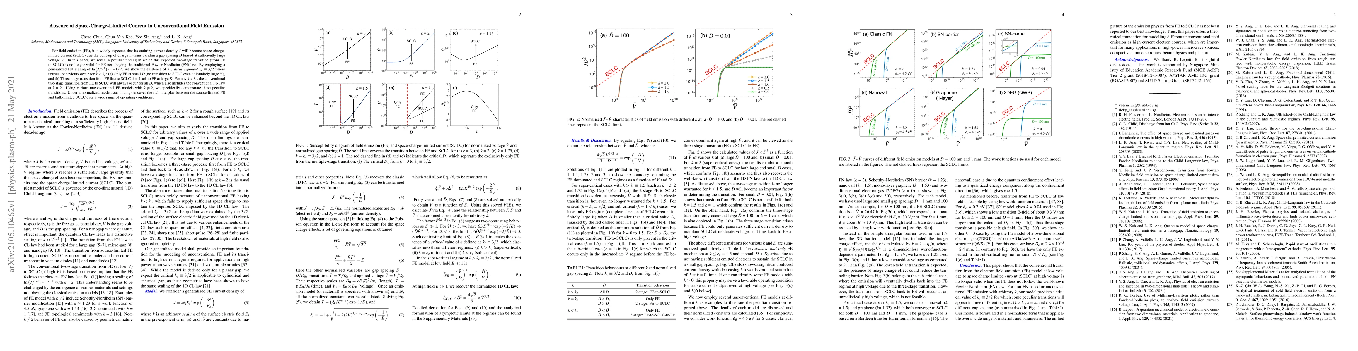
For field emission (FE), it is widely expected that its emitting current density $J$ will become space-charge-limited current (SCLC) due the built-up of charge in-transit within a gap spacing $D$ bi...
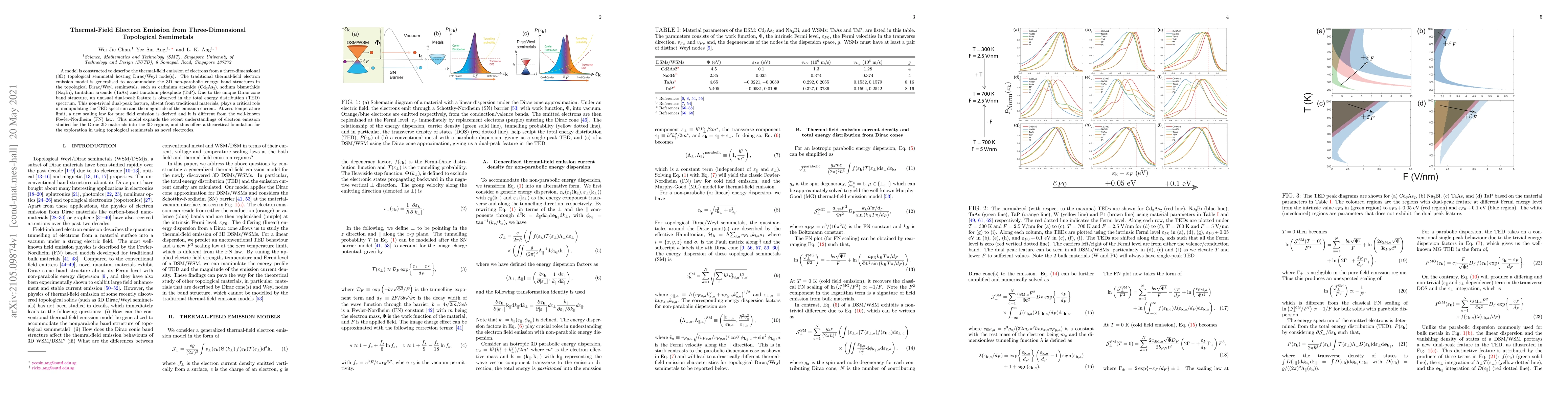
A model is constructed to describe the thermal-field emission of electrons from a three-dimensional ($3$D) topological semimetal hosting Dirac/Weyl node(s). The traditional thermal-field electron em...
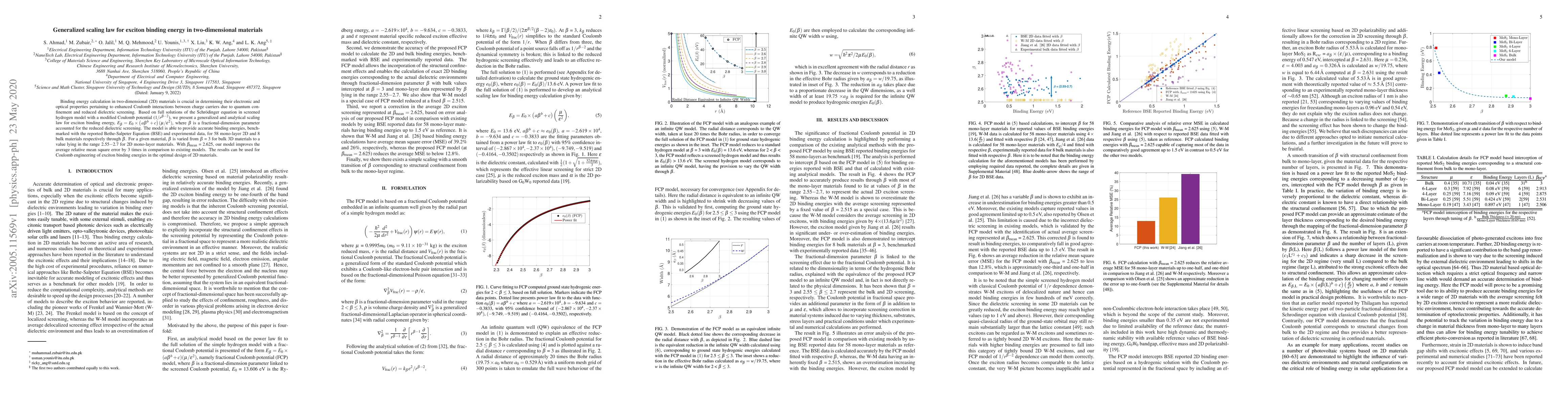
Binding energy calculation in two-dimensional (2D) materials is crucial in determining their electronic and optical properties pertaining to enhanced Coulomb interactions between charge carriers due...
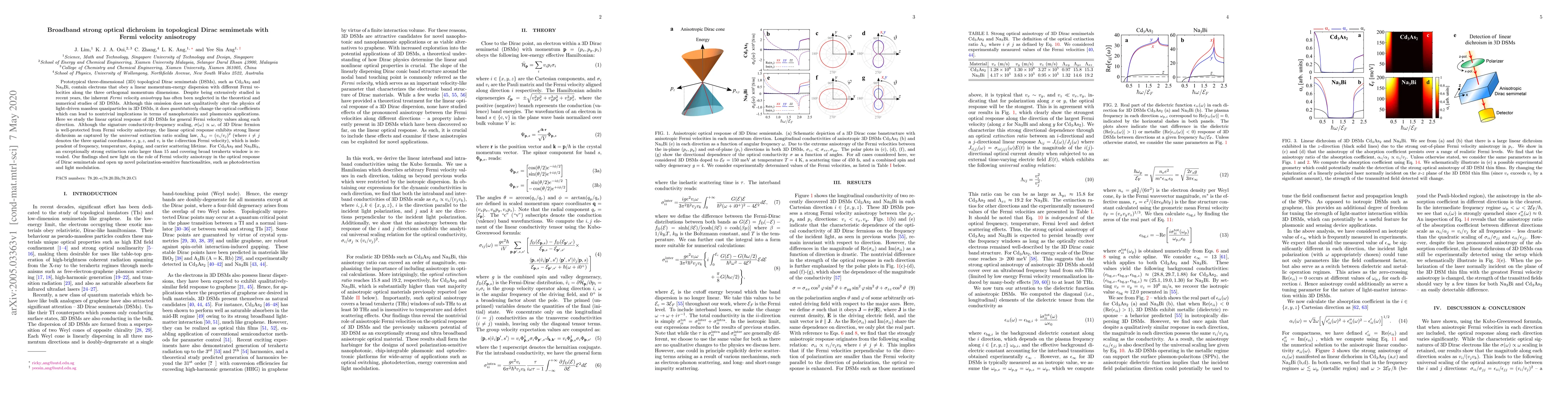
Prototypical three-dimensional (3D) topological Dirac semimetals (DSMs), such as Cd$_3$As$_2$ and Na$_3$Bi, contain electrons that obey a linear momentum-energy dispersion with different Fermi veloc...
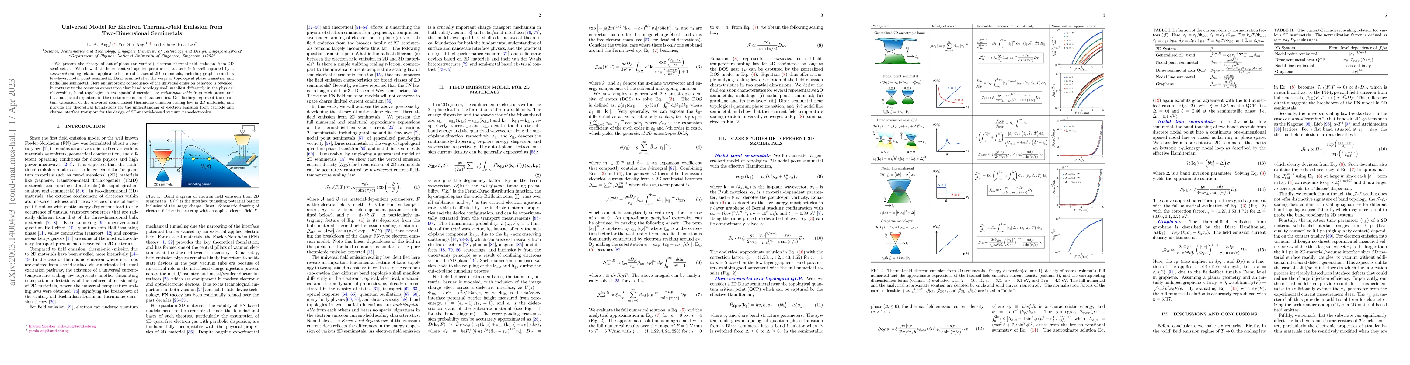
We present the theory of out-of-plane (or vertical) electron thermal-field emission from 2D semimetals. We show that the current-voltage-temperature characteristic is well-captured by a universal sc...
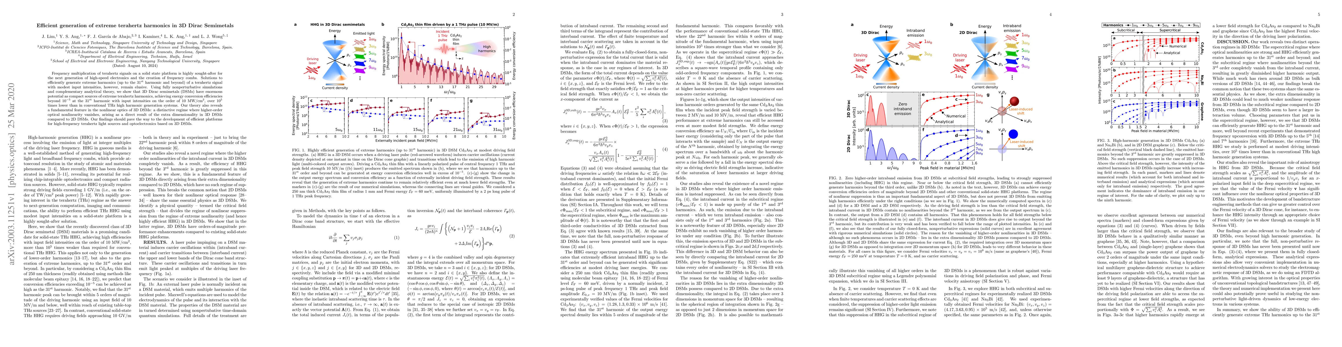
Frequency multiplication of terahertz signals on a solid state platform is highly sought-after for the next generation of high-speed electronics and the creation of frequency combs. Solutions to eff...
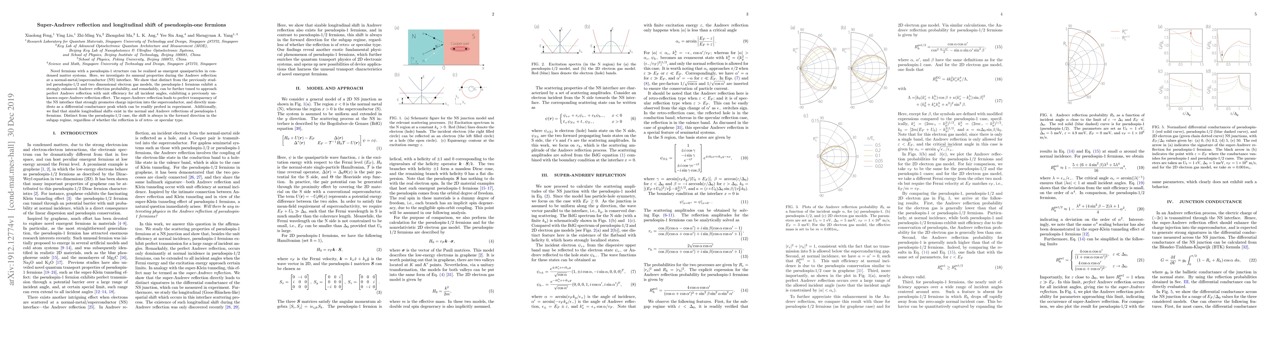
Novel fermions with a pseudospin-1 structure can be realized as emergent quasiparticles in condensed matter systems. Here, we investigate its unusual properties during the Andreev reflection at a no...
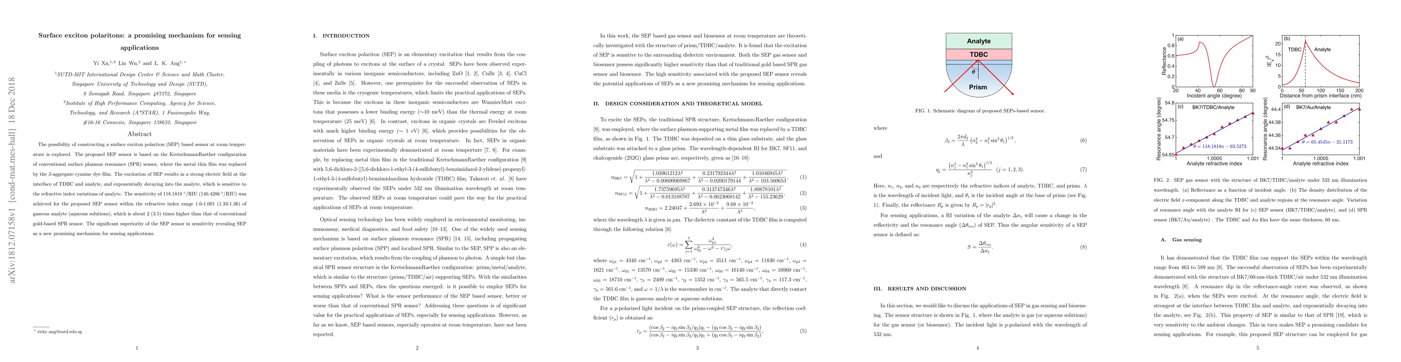
The possibility of constructing a surface exciton polariton (SEP) based sensor at room temperature is explored. The proposed SEP sensor is based on the Kretschmann-Raether configuration of conventio...
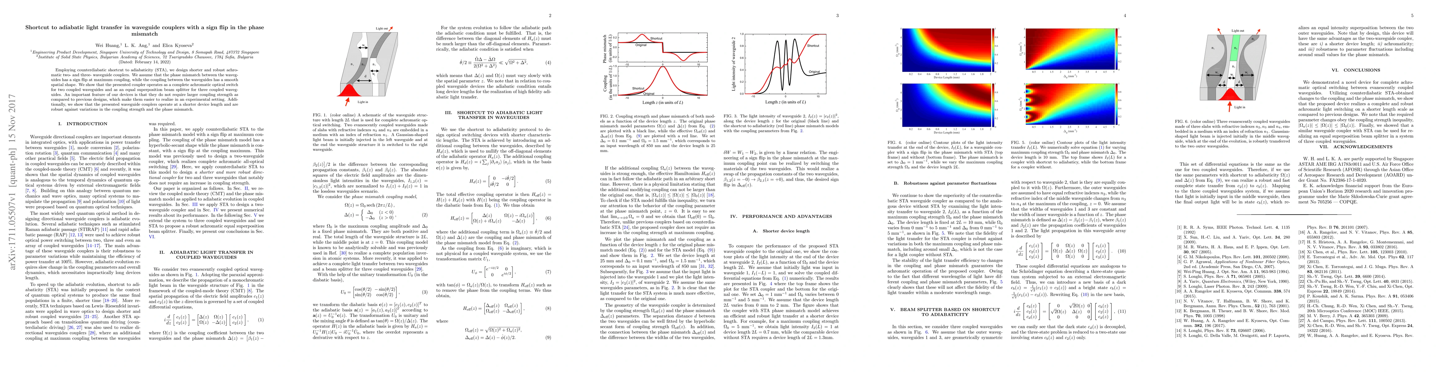
Employing counterdiabatic shortcut to adiabaticity (STA), we design shorter and robust achromatic two- and three- waveguide couplers. We assume that the phase mismatch between the waveguides has a s...
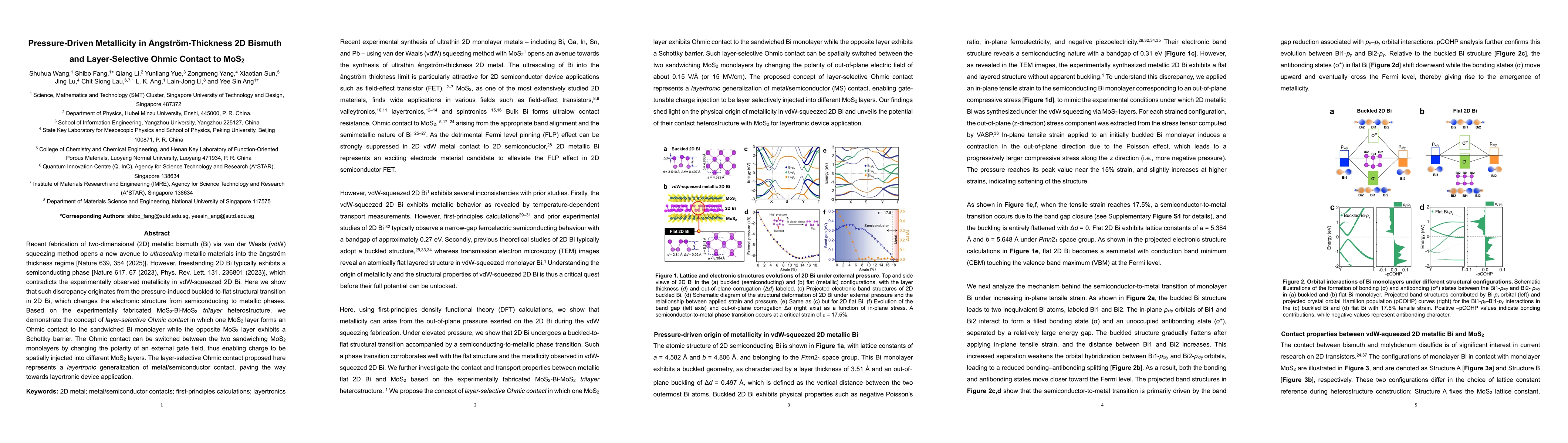
Recent fabrication of two-dimensional (2D) metallic bismuth (Bi) via van der Waals (vdW) squeezing method opens a new avenue to ultrascaling metallic materials into the {\aa}ngstr\"om-thickness regime...
Advancing complementary metal-oxide-semiconductor (CMOS) technology into the sub-1-nm angstr\"om-scale technology nodes is expected to involve alternative semiconductor channel materials, as silicon t...