Academic Profile
Statistics
Similar Authors
Papers on arXiv
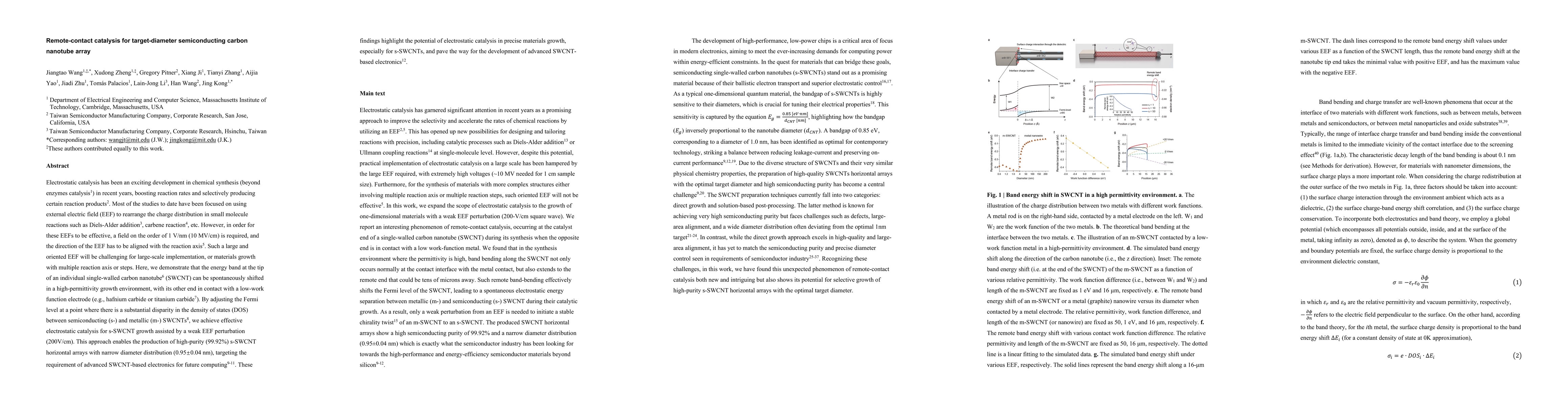
Electrostatic catalysis has been an exciting development in chemical synthesis (beyond enzymes catalysis) in recent years, boosting reaction rates and selectively producing certain reaction products...
Monolayer hBN has attracted interest as a potentially weakly interacting 2D insulating layer in heterostructures. Recently, wafer-scale hBN growth on Cu(111) has been demonstrated for semiconductor ...
The 3D local atomic structures and crystal defects at the interfaces of heterostructures control their electronic, magnetic, optical, catalytic and topological quantum properties, but have thus far ...
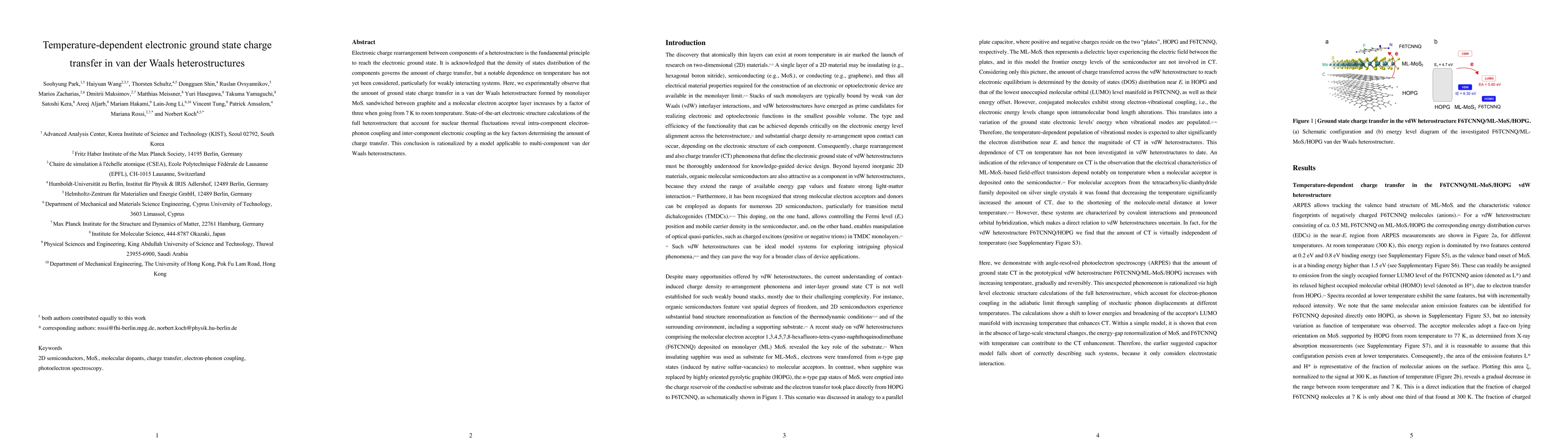
Electronic charge rearrangement between components of a heterostructure is the fundamental principle to reach the electronic ground state. It is acknowledged that the density of states distribution ...
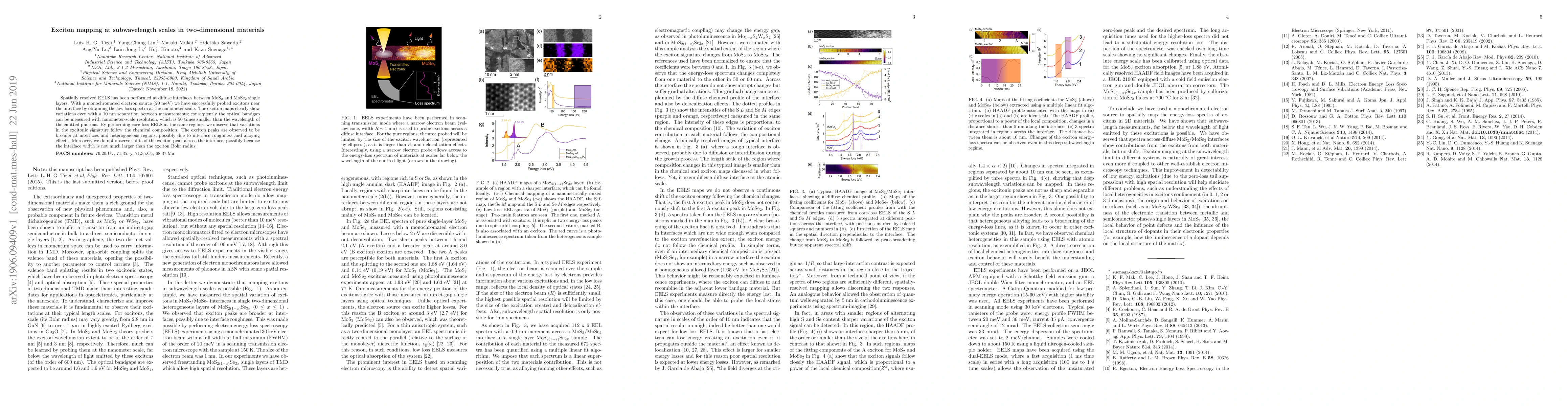
Spatially resolved EELS has been performed at diffuse interfaces between MoS$_2$ and MoSe$_2$ single layers. With a monochromated electron source (20 meV) we have successfully probed excitons near t...
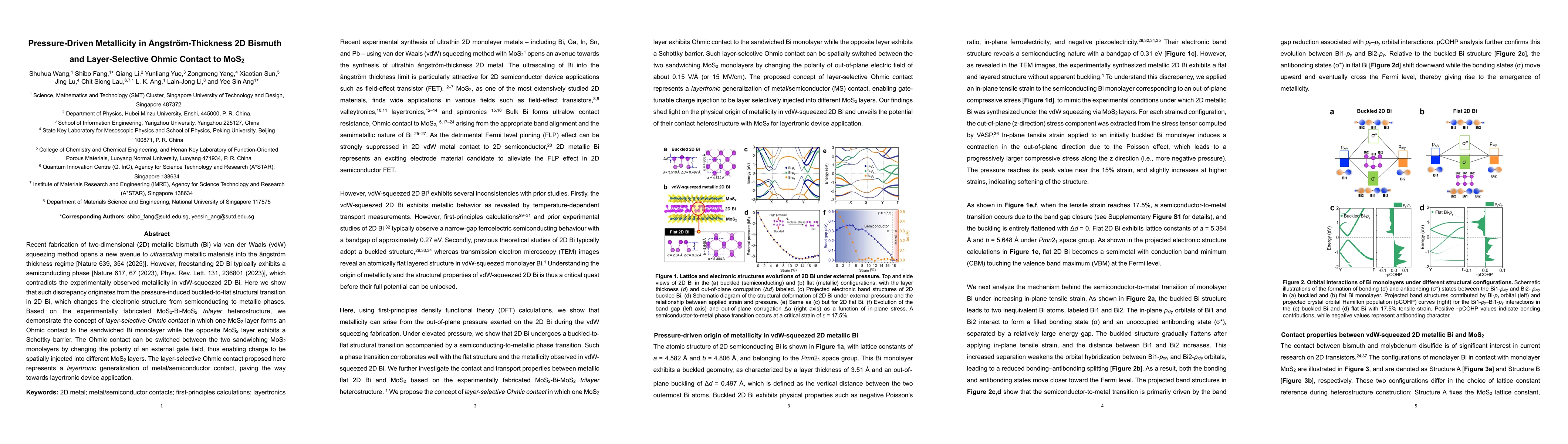
Recent fabrication of two-dimensional (2D) metallic bismuth (Bi) via van der Waals (vdW) squeezing method opens a new avenue to ultrascaling metallic materials into the {\aa}ngstr\"om-thickness regime...
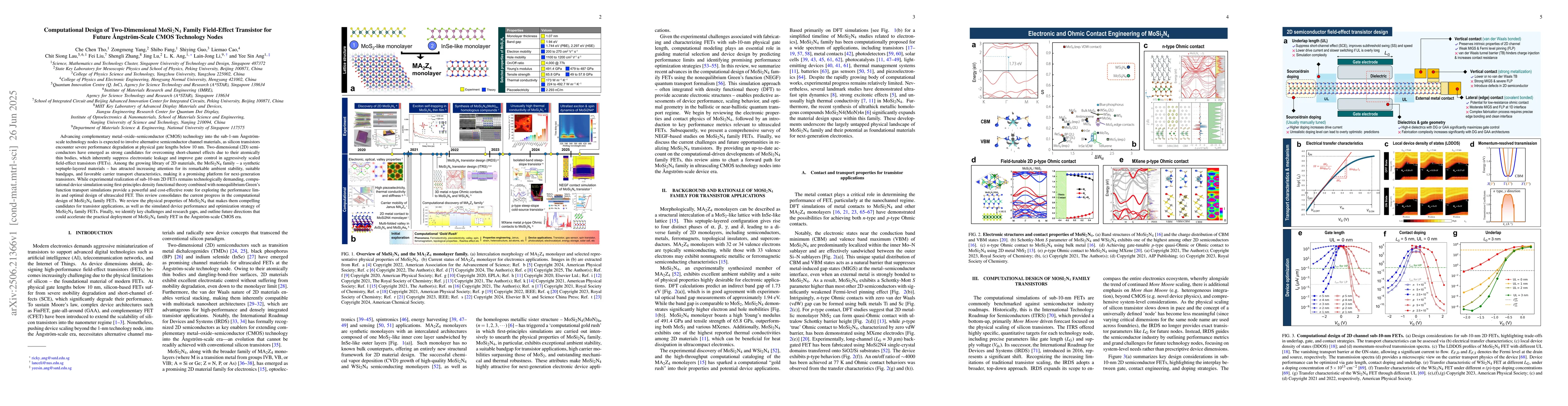
Advancing complementary metal-oxide-semiconductor (CMOS) technology into the sub-1-nm angstr\"om-scale technology nodes is expected to involve alternative semiconductor channel materials, as silicon t...
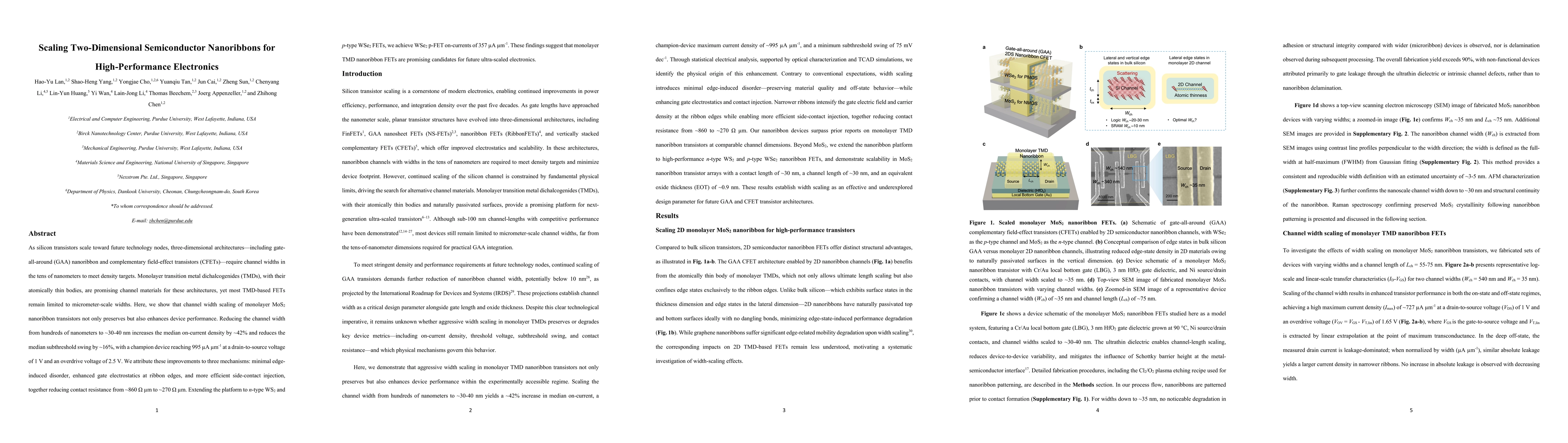
Monolayer transition metal dichalcogenide (TMD) field-effect transistors (FETs), with their atomically thin bodies, are promising candidates for future gate-all-around (GAA) nanoribbon architectures. ...
2D van der Waals ferroelectrics, particularly alpha-In2Se3, have emerged as an attractive building block for next-generation information storage technologies due to their moderate band gap and robust ...
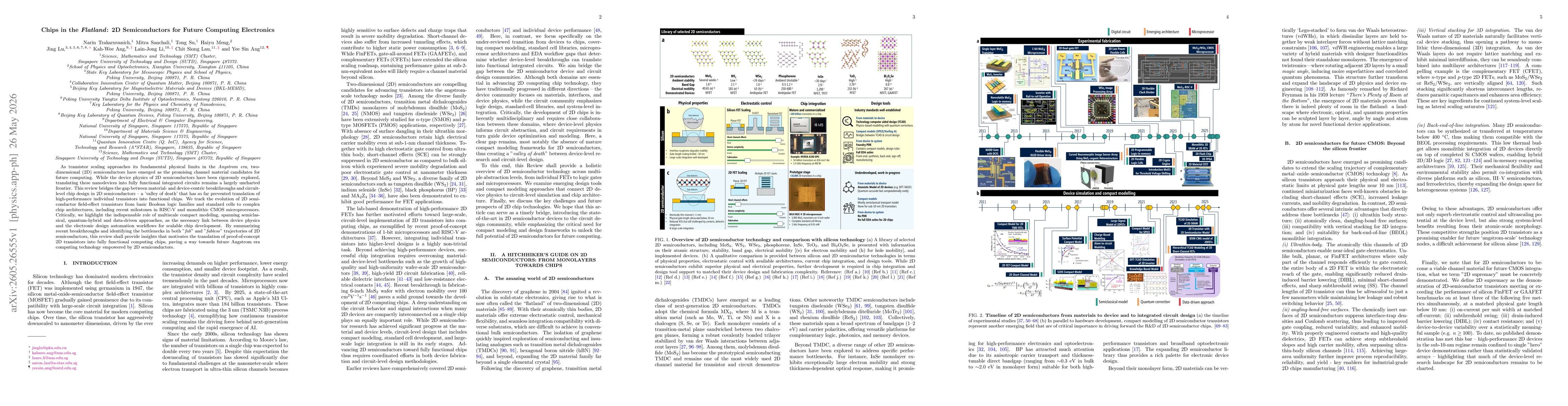
As transistor scaling approaches its fundamental physical limits in the Angstrom era, two-dimensional (2D) semiconductors have emerged as the promising channel material candidates for future computing...