Academic Profile
Statistics
Similar Authors
Papers on arXiv
For the past few years, 2D ferroelectric materials have attracted strong interest for their potential in future nanoelectronics devices. The recent discovery of 2D ferroelectricity in twisted layers...
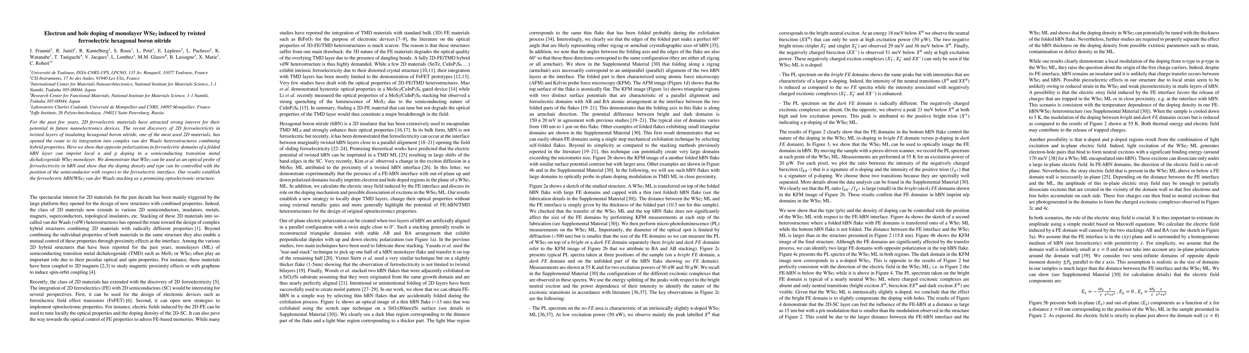
Being able to control the neutral excitonic flux is a mandatory step for the development of future room-temperature two-dimensional excitonic devices. Semiconducting Monolayer Transition Metal Dicha...
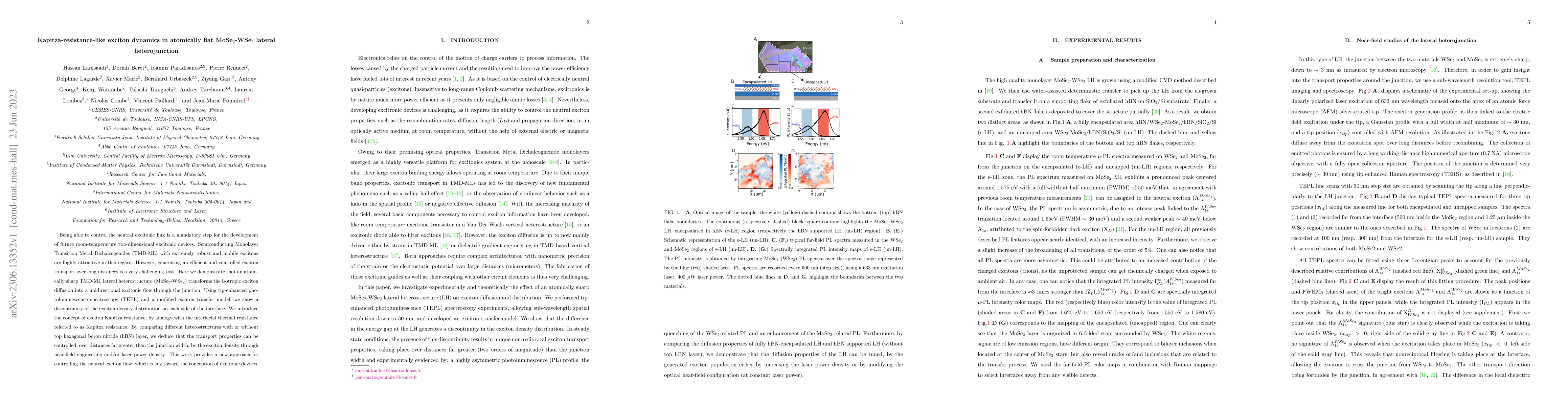
The existence of bound charge transfer (CT) excitons at the interface of monolayer lateral heterojunctions has been debated in literature, but contrary to the case of interlayer excitons in vertical...
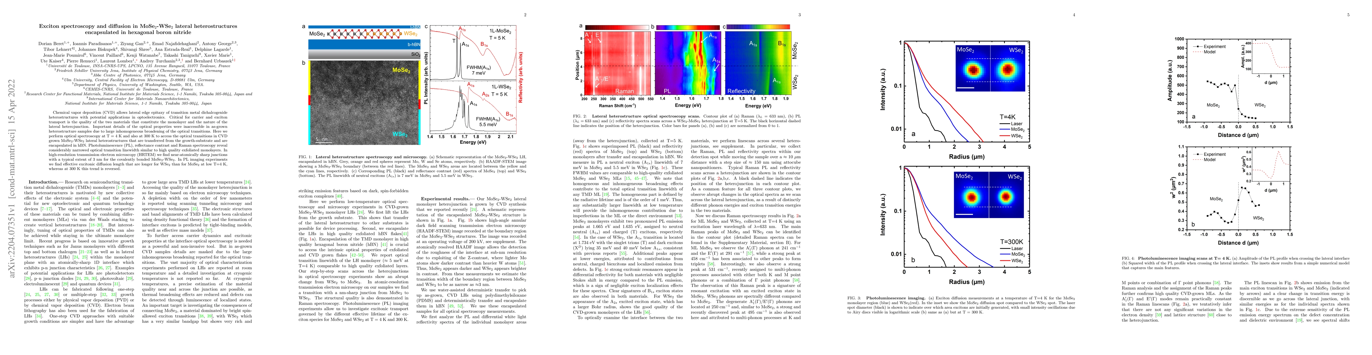
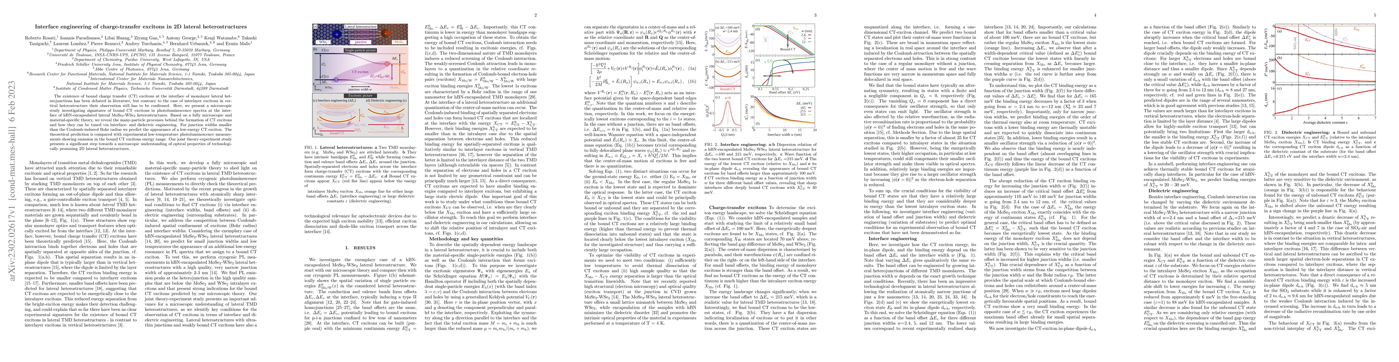
Chemical vapor deposition (CVD) allows lateral edge epitaxy of transition metal dichalcogenide heterostructures with potential applications in optoelectronics. Critical for carrier and exciton trans...
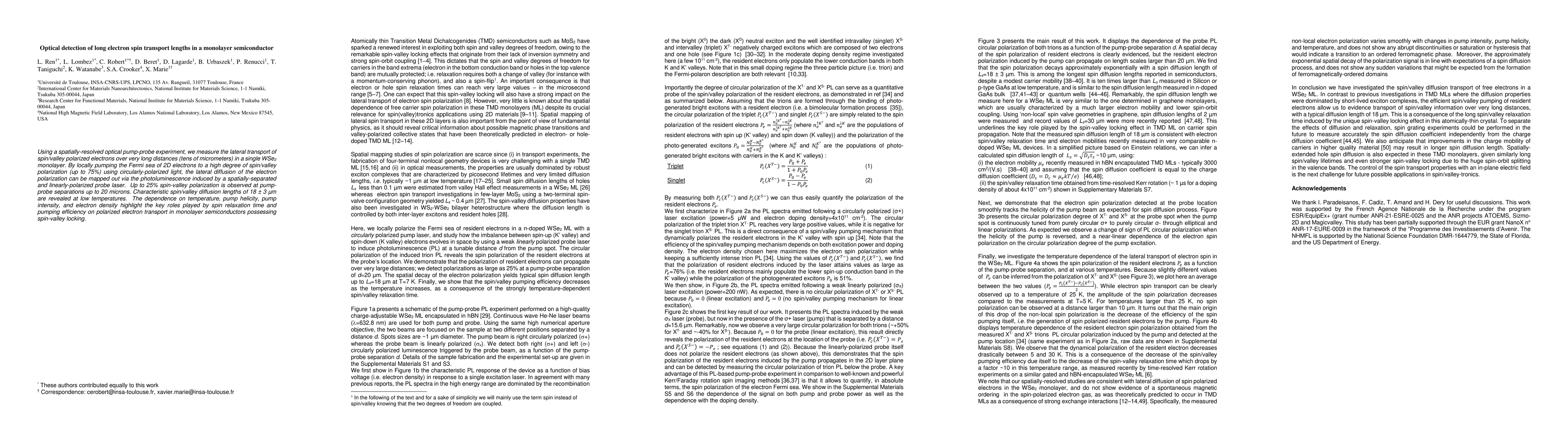
Using a spatially-resolved optical pump-probe experiment, we measure the lateral transport of spin/valley polarized electrons over very long distances (tens of micrometers) in a single WSe2 monolaye...
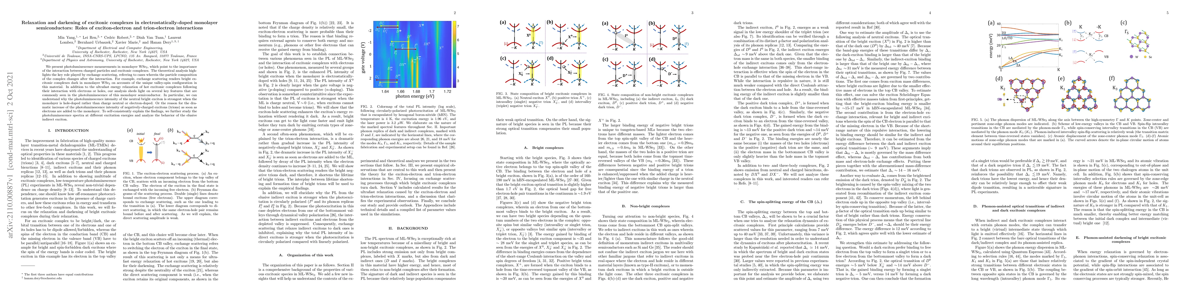
We present photoluminescence measurements in monolayer WSe$_2$, which point to the importance of the interaction between charged particles and excitonic complexes. The theoretical analysis highlight...
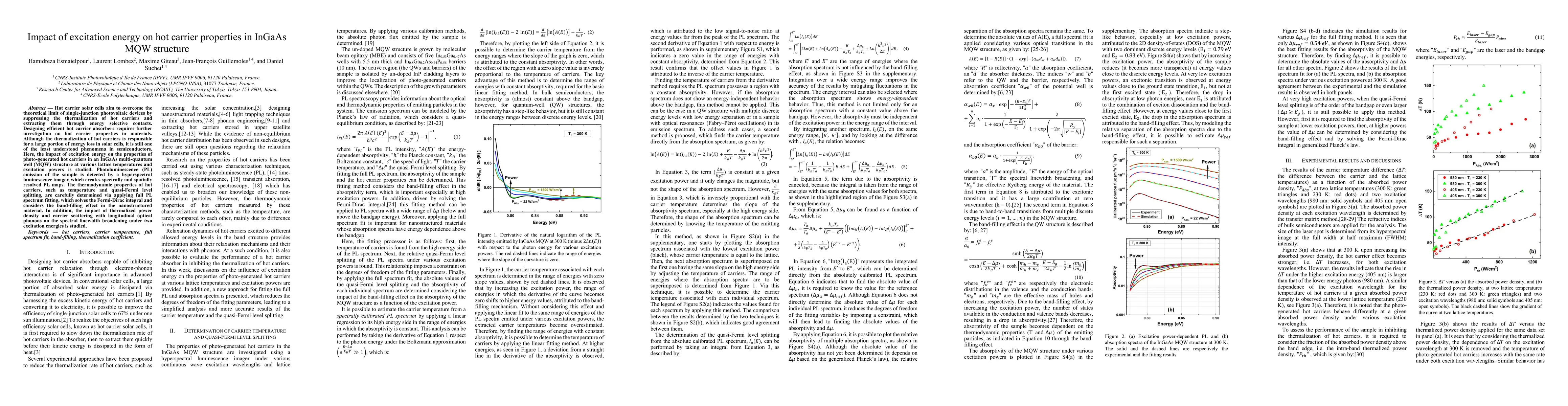
Hot carrier solar cells aim to overcome the theoretical limit of single-junction photovoltaic devices by suppressing the thermalization of hot carriers and extracting them through energy selective c...
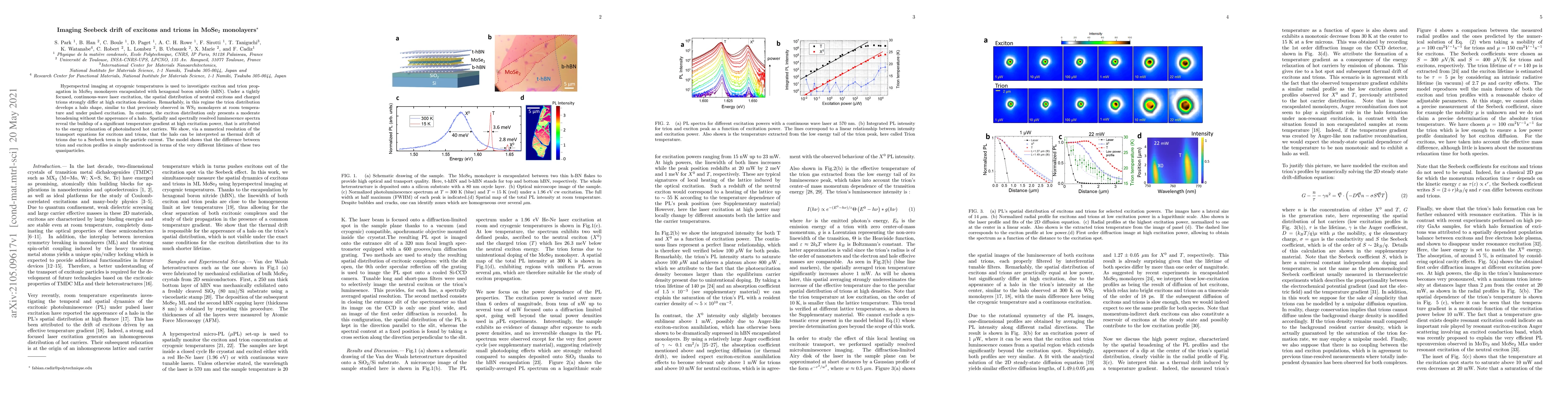
Hyperspectral imaging at cryogenic temperatures is used to investigate exciton and trion propagation in MoSe$_2$ monolayers encapsulated with hexagonal boron nitride (hBN). Under a tightly focused, ...
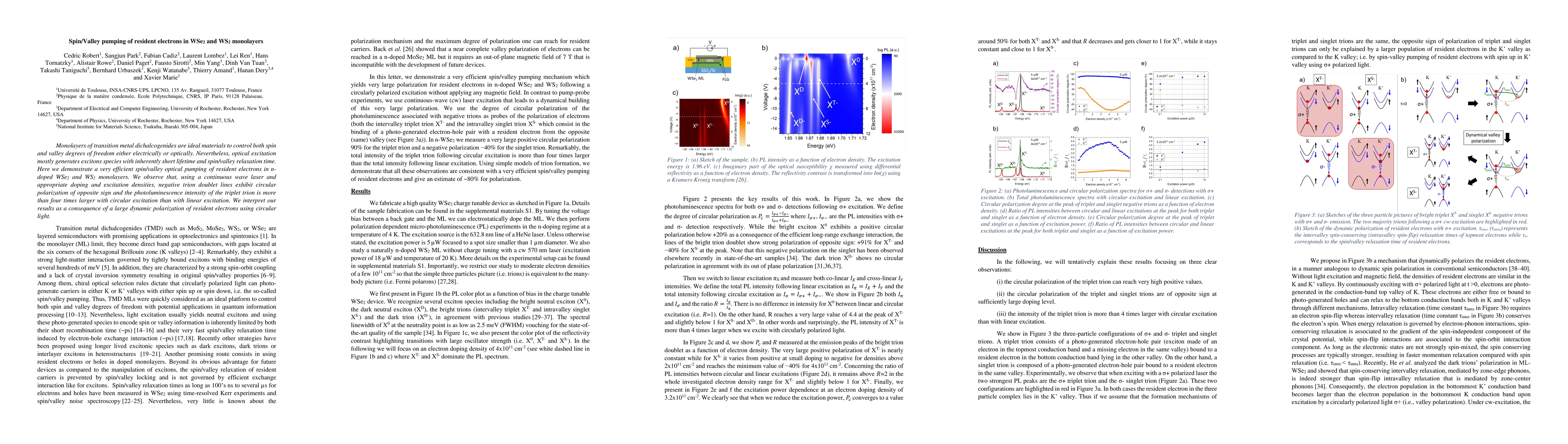
Monolayers of transition metal dichalcogenides are ideal materials to control both spin and valley degrees of freedom either electrically or optically. Nevertheless, optical excitation mostly genera...
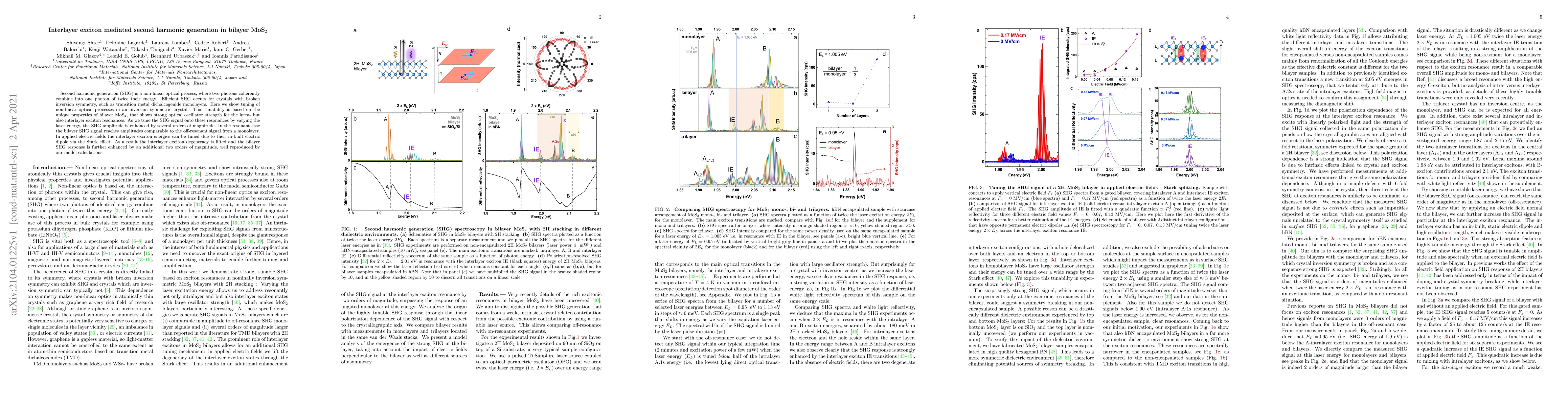
Second harmonic generation (SHG) is a non-linear optical process, where two photons coherently combine into one photon of twice their energy. Efficient SHG occurs for crystals with broken inversion ...
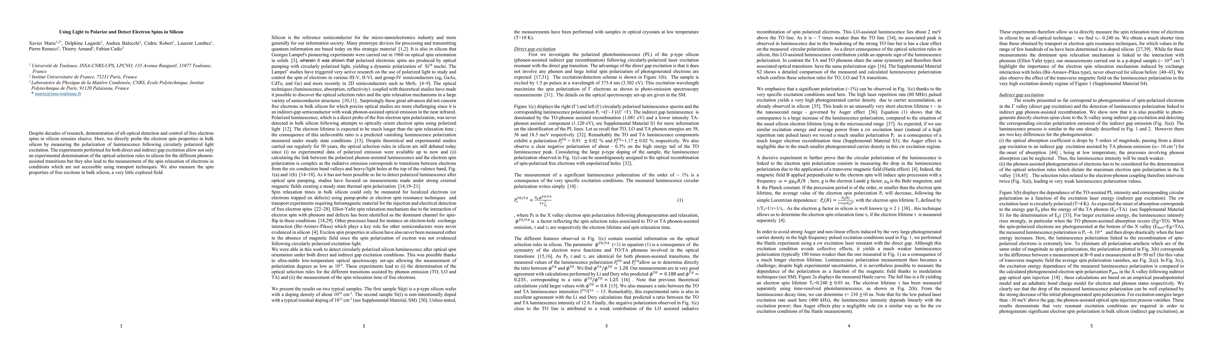
Despite decades of research, demonstration of all-optical detection and control of free electron spins in silicon remains elusive. Here, we directly probe the electron spin properties in bulk silicon ...
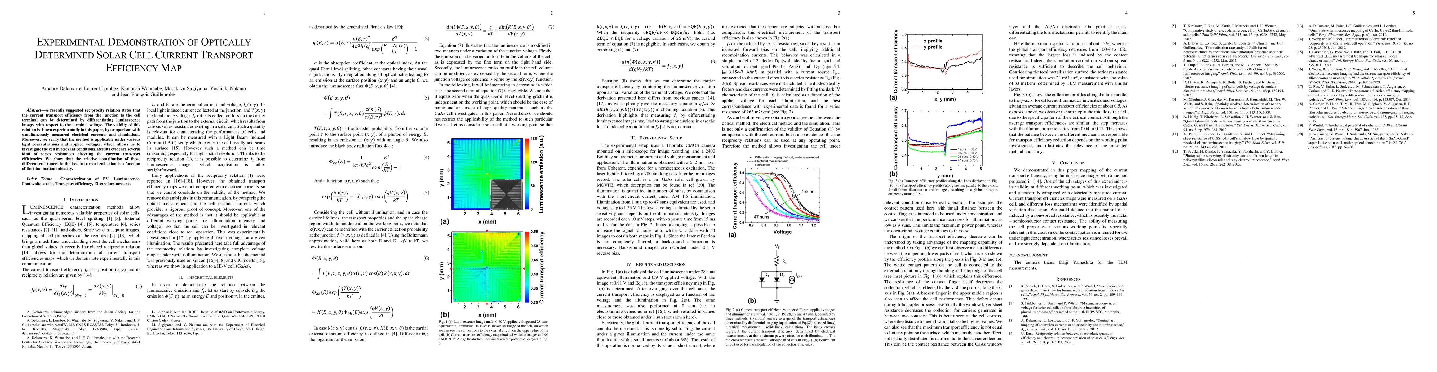
A recently suggested reciprocity relation states that the current transport efficiency from the junction to the cell terminal can be determined by differentiating luminescence images with respect to t...
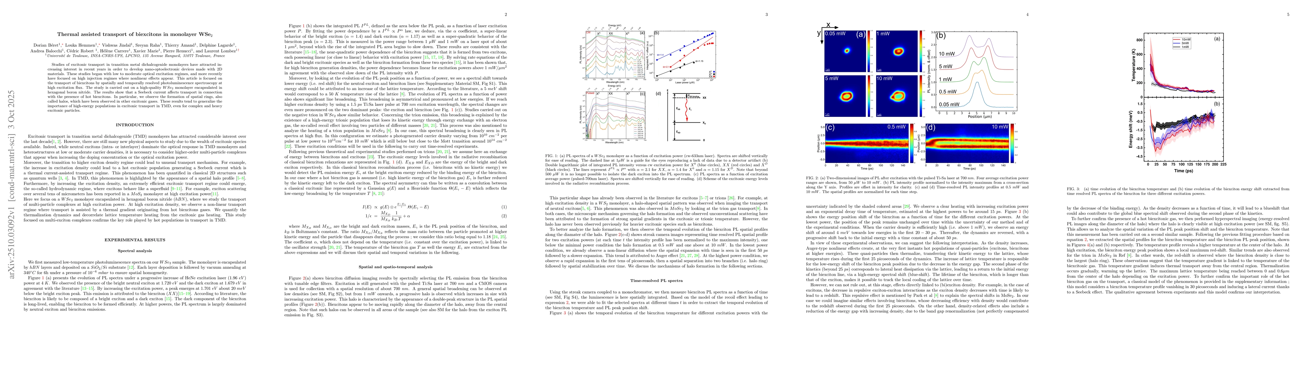
Studies of excitonic transport in transition metal dichalcogenide monolayers have attracted increasing interest in recent years in order to develop nano-optoelectronic devices made with 2D materials. ...
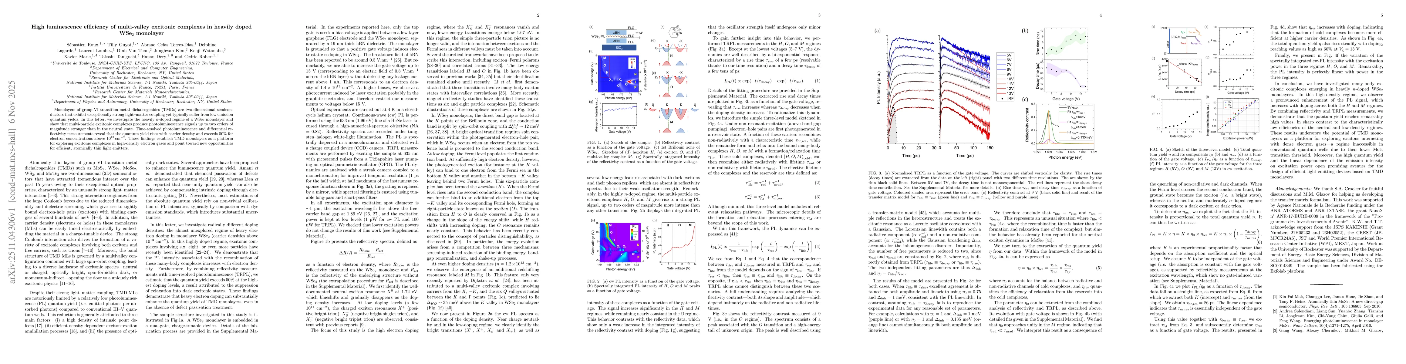
Monolayers of group-VI transition-metal dichalcogenides (TMDs) are two-dimensional semiconductors that exhibit exceptionally strong light-matter coupling yet typically suffer from low emission quantum...
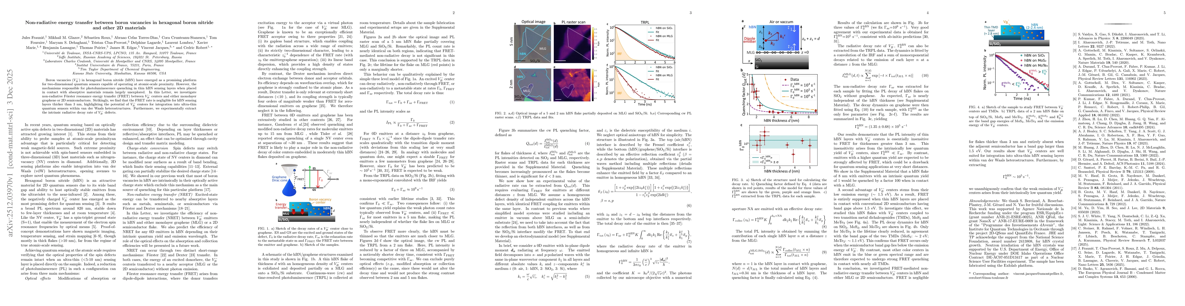
Boron vacancies ($V_B^-$) in hexagonal boron nitride (hBN) have emerged as a promising platform for two-dimensional quantum sensors capable of operating at atomic-scale proximity. However, the mechani...