Academic Profile
Statistics
Similar Authors
Papers on arXiv
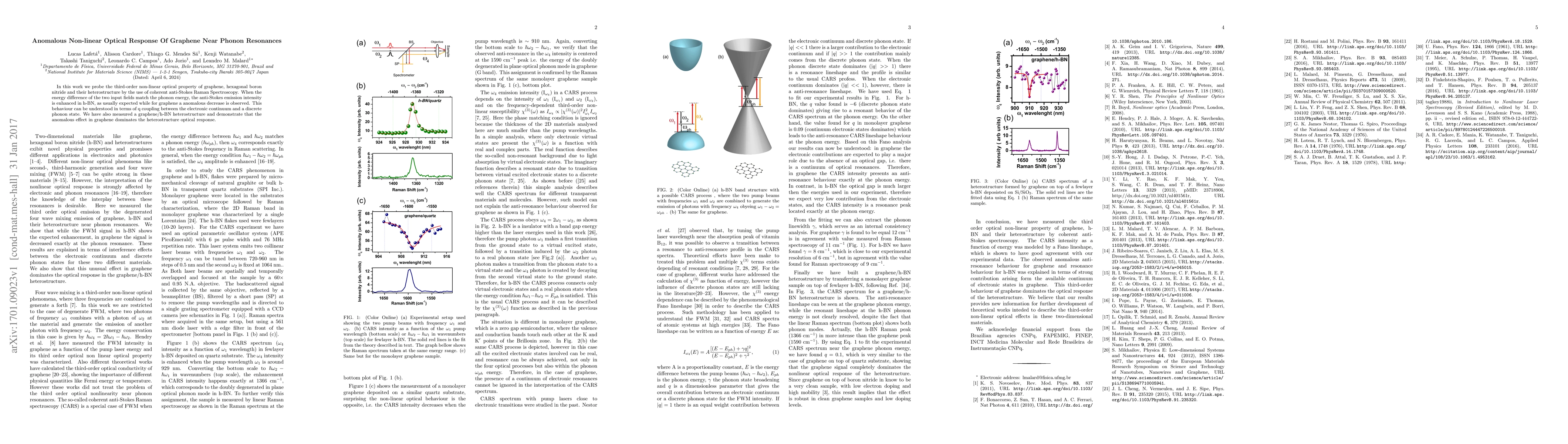
In this work we probe the third-order non-linear optical property of graphene, hexagonal boron nitride and their heterostructure by the use of coherent anti-Stokes Raman Spectroscopy. When the energ...
Transition metal dichalcogenide (TMD) monolayers present a singular coupling in their spin and valley degrees of freedom. Moreover, by applying an external magnetic field it is possible to break the...
The role of defects in two-dimensional semiconductors and how they affect the intrinsic properties of these materials have been a wide researched topic over the past decades. Optical characterizatio...
Two-dimensional dilute magnetic semiconductors has been recently reported in semiconducting transition metal dichalcogenides by the introduction of spin-polarized transition metal atoms as dopants. ...
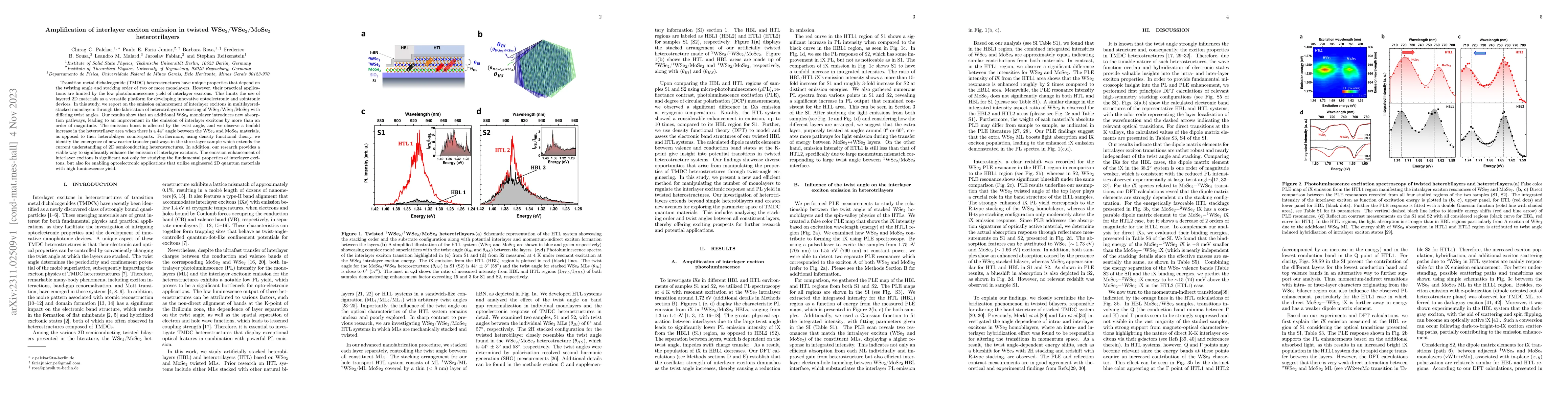
Transition metal dichalcogenide (TMDC) heterostructures have unique properties that depend on the twisting angle and stacking order of two or more monolayers. However, their practical applications a...
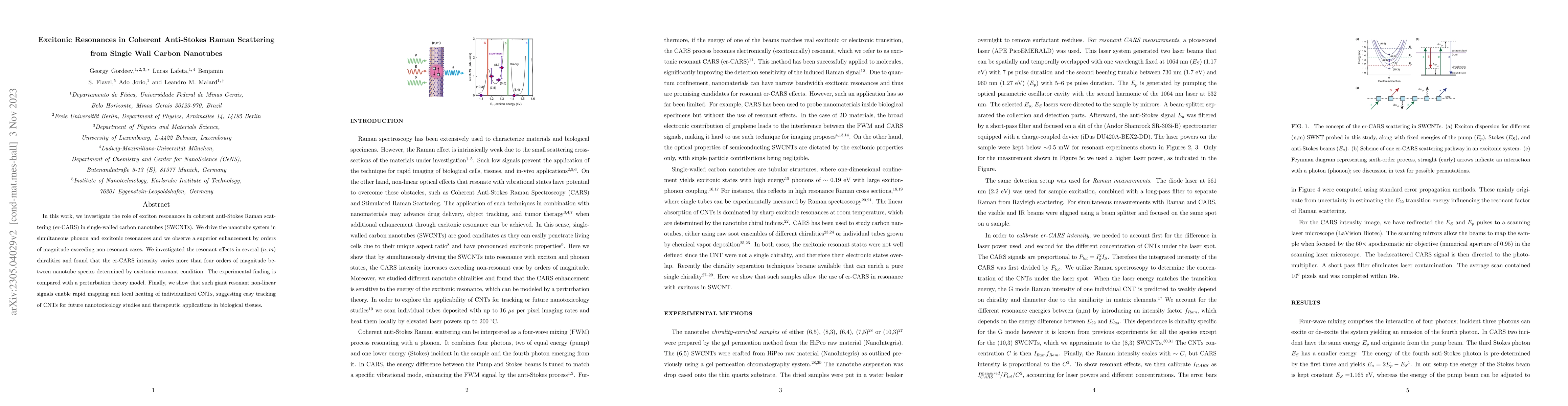
In this work we investigate the role of exciton resonances in coherent anti-Stokes Raman scattering (er-CARS) in single walled carbon nanotubes (SWCNTs). We drive the nanotube system in simultaneous...
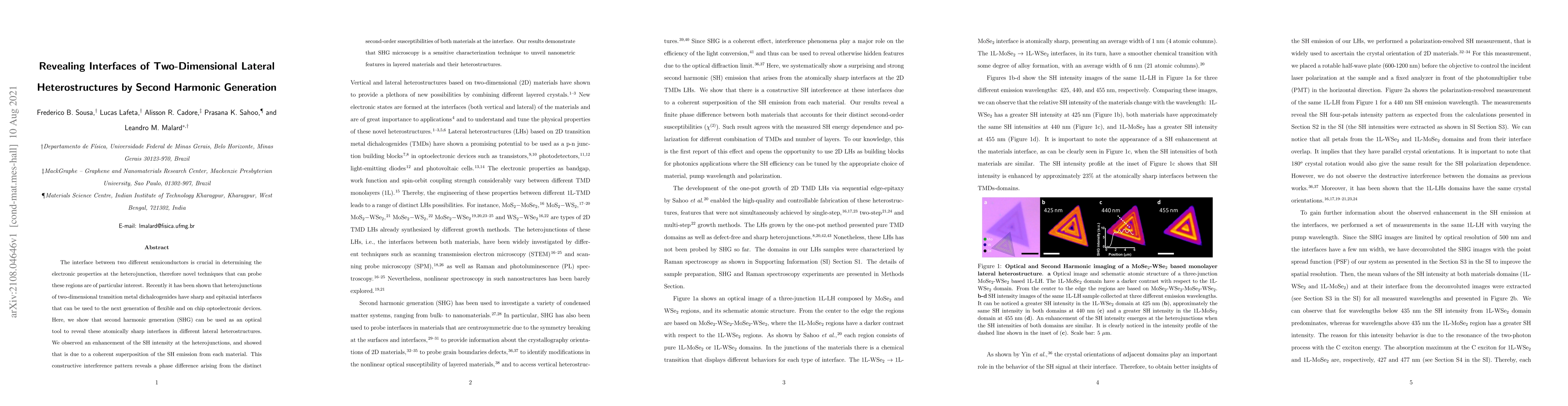
The interface between two different semiconductors is crucial in determining the electronic properties at the heterojunction, therefore novel techniques that can probe these regions are of particula...
![Thumbnail for Multimodal microscopy for characterization of
amyloid-${\unicode[Times]{x3B2}}$ plaques biomarkers in animal model of
Alzheimer's disease](https://nbg1.your-objectstorage.com/arxivlens/thumbnails/2102.03993.webp)
Given the long subclinical stage of Alzheimer's disease (AD), the study of biomarkers is relevant both for early diagnosis and the fundamental understanding of the pathophysiology of AD. Biomarkers ...
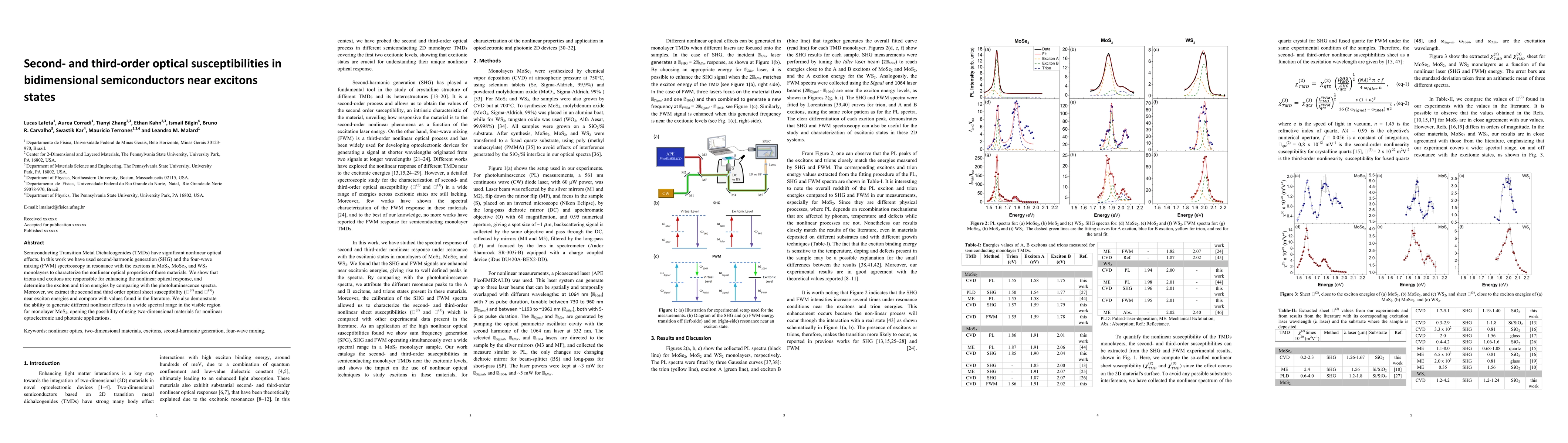
Semiconducting Transition Metal Dichalcogenides (TMDs) have significant nonlinear optical effects. In this work we have used second-harmonic generation (SHG) and the four-wave mixing (FWM) spectrosc...
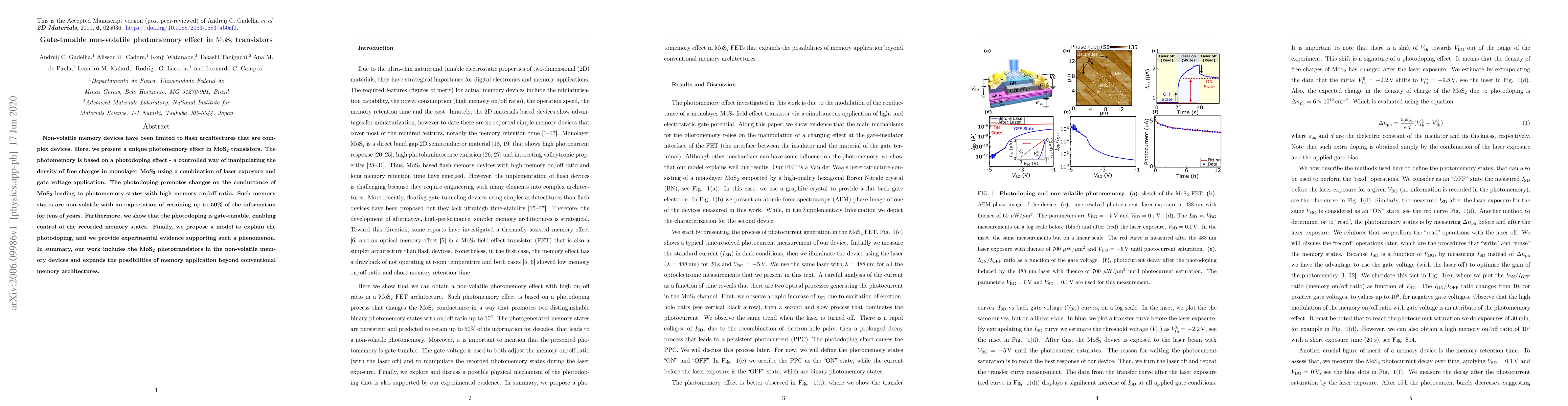
Non-volatile memory devices have been limited to flash architectures that are complex devices. Here, we present a unique photomemory effect in MoS$_2$ transistors. The photomemory is based on a phot...
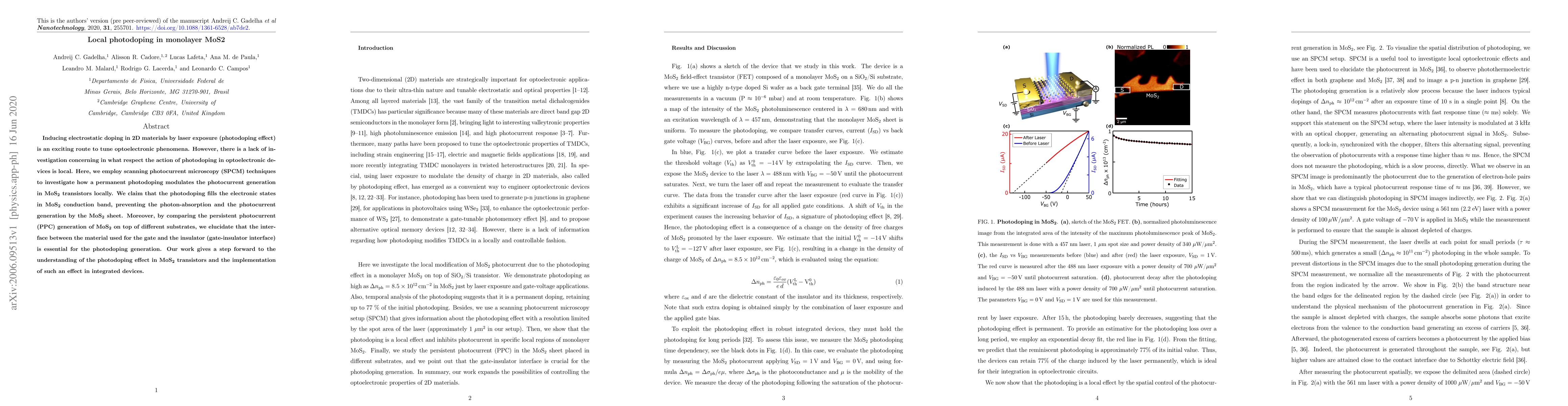
Inducing electrostatic doping in 2D materials by laser exposure (photodoping effect) is an exciting route to tune optoelectronic phenomena. However, there is a lack of investigation concerning in wh...
Extended defects with one dimensionality smaller than that of the host, such as 2D grain boundaries in 3D materials or 1D grain boundaries in 2D materials, can be particularly damaging since they di...
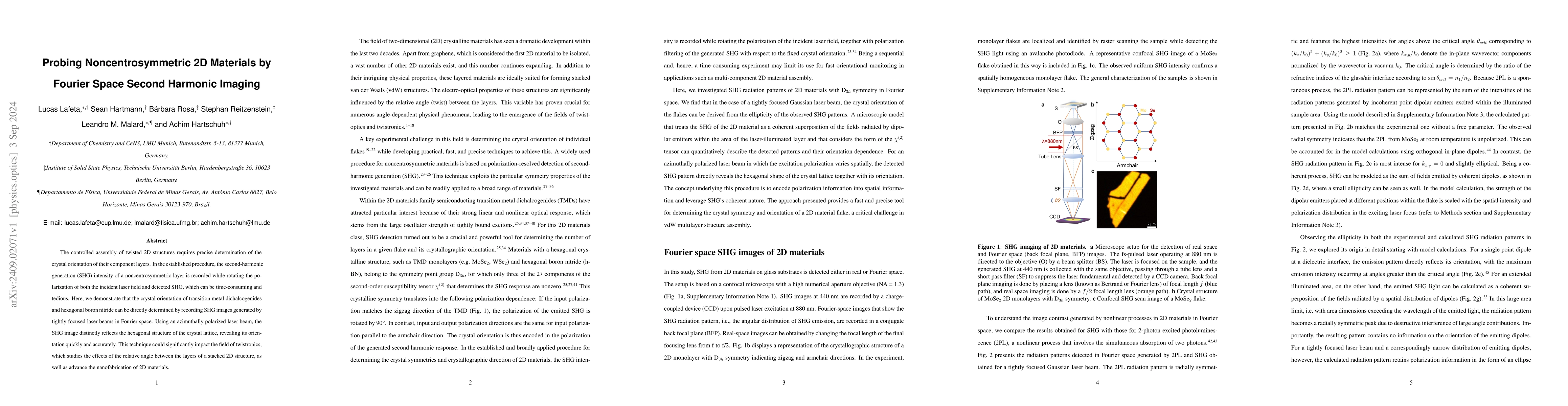
The controlled assembly of twisted 2D structures requires precise determination of the crystal orientation of their component layers. In the established procedure, the second-harmonic generation (SHG)...
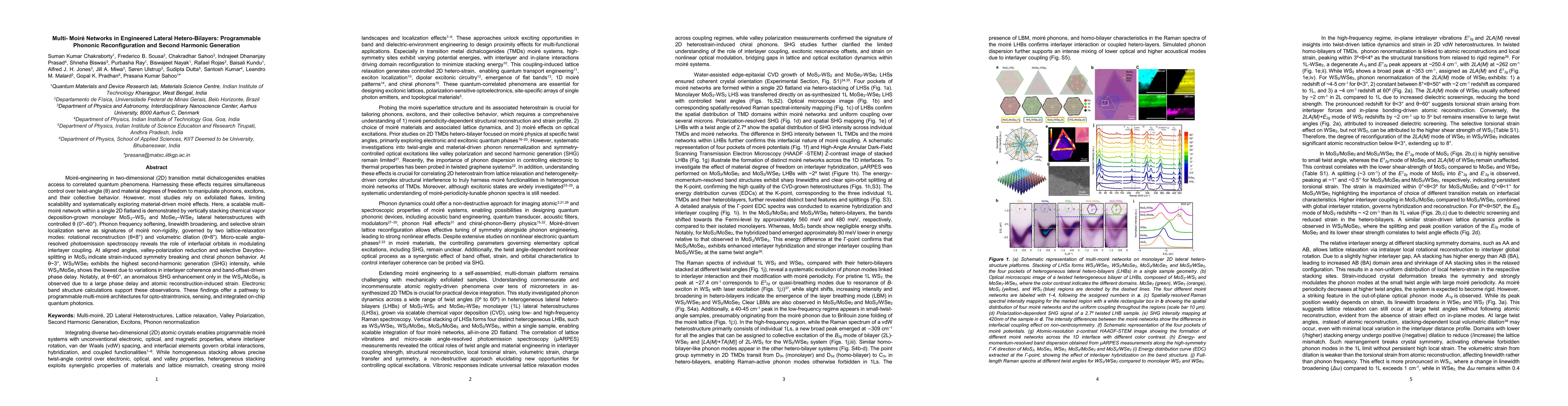
Moire engineering in two-dimensional transition metal dichalcogenides enables access to correlated quantum phenomena. Realizing such effects demands simultaneous control over twist angle and material ...
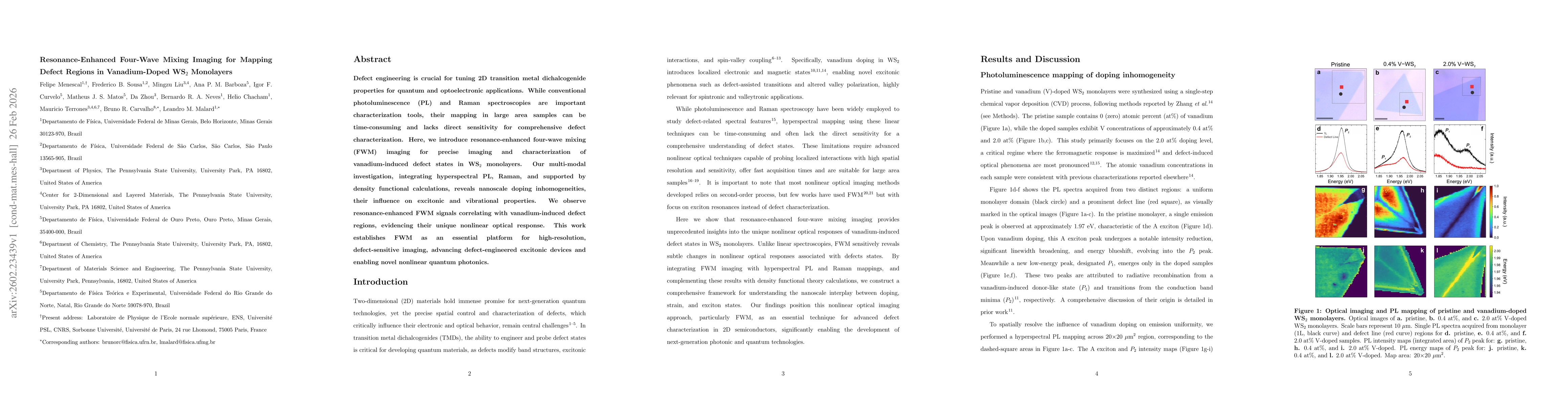
Defect engineering is crucial for tuning 2D transition metal dichalcogenide properties for quantum and optoelectronic applications. While conventional photoluminescence (PL) and Raman spectroscopies a...
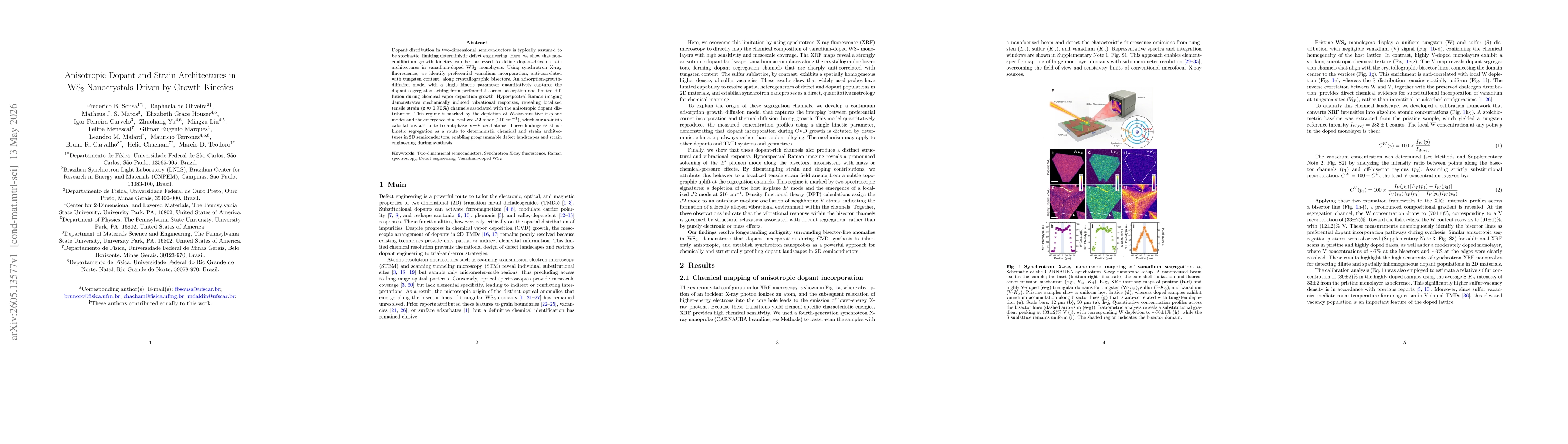
Dopant distribution in two-dimensional semiconductors is typically assumed to be stochastic, limiting deterministic defect engineering. Here, we show that non-equilibrium growth kinetics can be harnes...