Academic Profile
Statistics
Similar Authors
Papers on arXiv
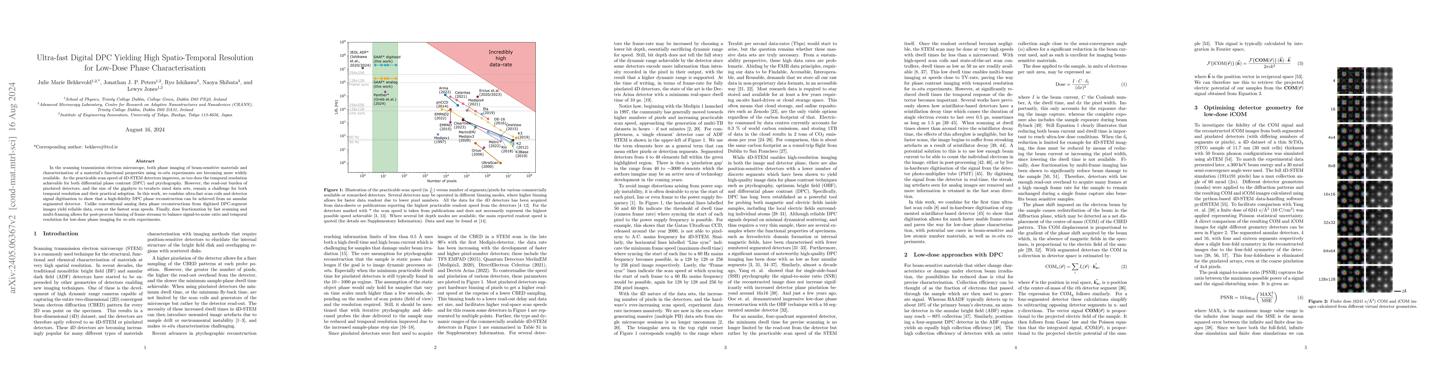
In the scanning transmission electron microscope, both phase imaging of beam-sensitive materials and characterisation of a material's functional properties using in-situ experiments are becoming mor...
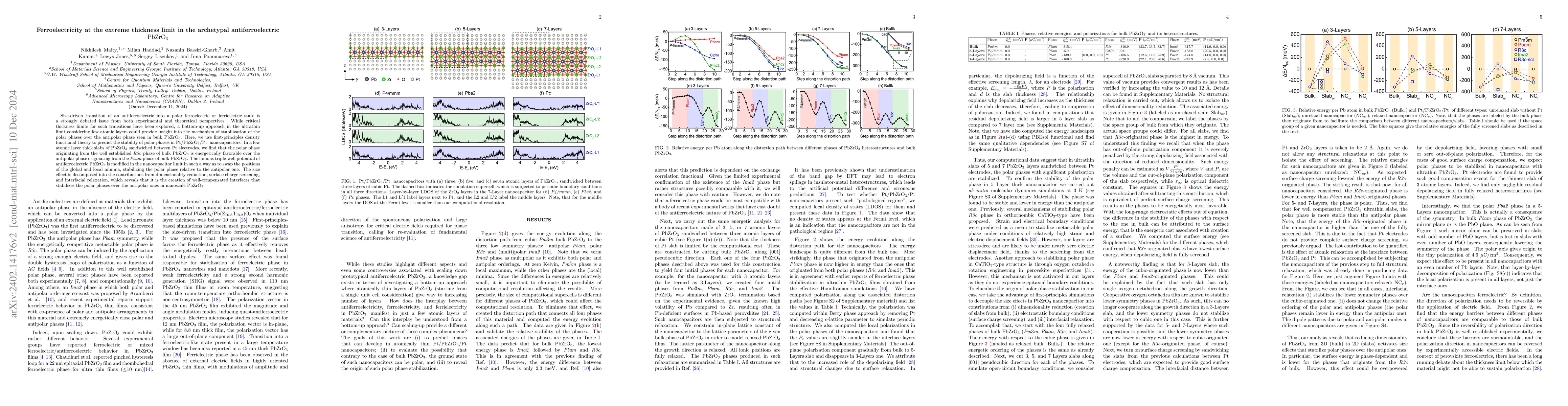
Size-driven transition of an antiferroelectric into a polar ferroelectric or ferrielectric state is a strongly debated issue from both experimental and theoretical perspectives. While critical thick...
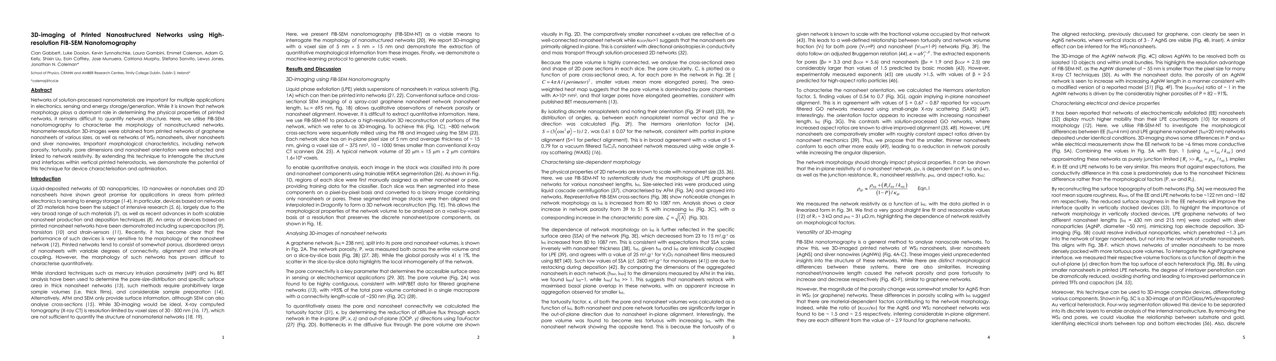
Networks of solution-processed nanomaterials are important for multiple applications in electronics, sensing and energy storage/generation. While it is known that network morphology plays a dominant...
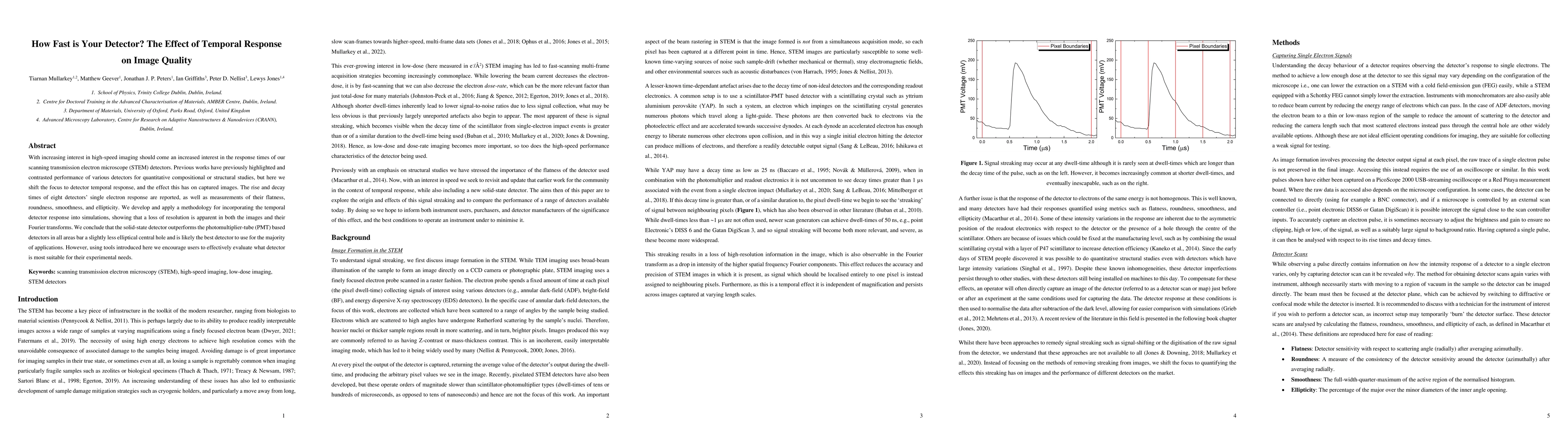
With increasing interest in high-speed imaging should come an increased interest in the response times of our scanning transmission electron microscope (STEM) detectors. Previous works have previous...
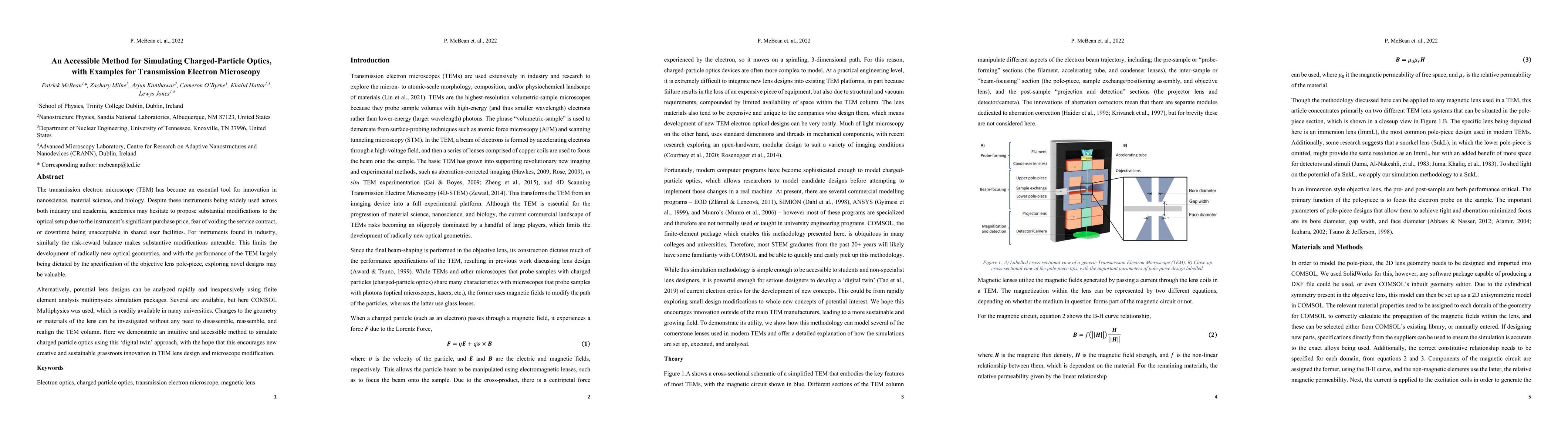
The transmission electron microscope (TEM) has become an essential tool for innovation in nanoscience, material science, and biology. Despite these instruments being widely used across both industry...
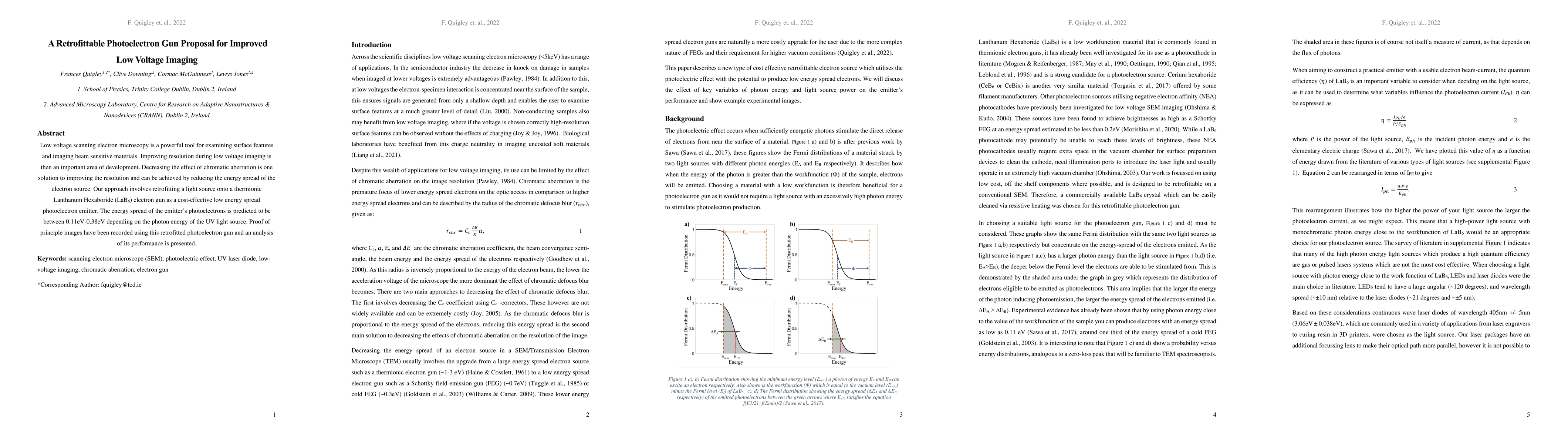
Low voltage scanning electron microscopy is a powerful tool for examining surface features and imaging beam sensitive materials. Improving resolution during low voltage imaging is then an important ...
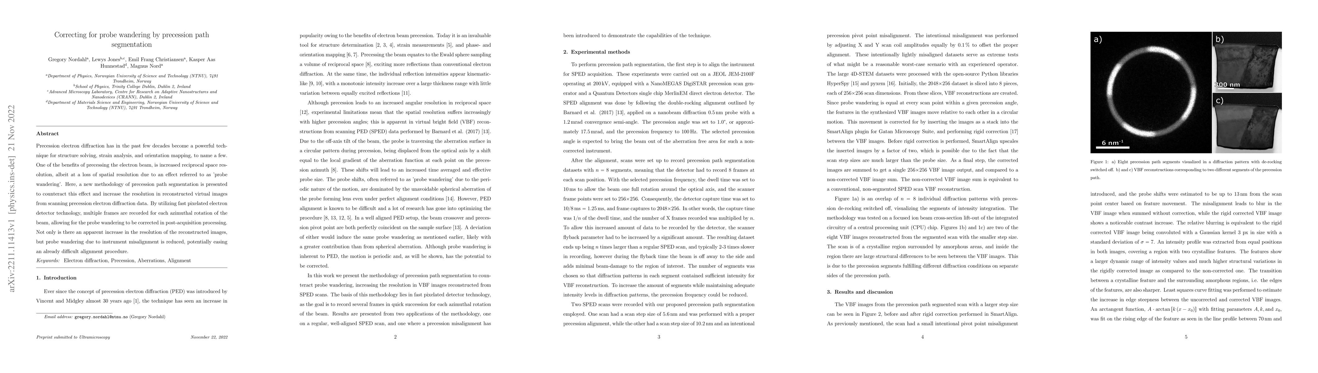
Precession electron diffraction has in the past few decades become a powerful technique for structure solving, strain analysis, and orientation mapping, to name a few. One of the benefits of precess...
Fast frame-rates are desirable in scanning transmission electron microscopy for a number of reasons: controlling electron beam dose, capturing in-situ events or reducing the appearance of scan disto...
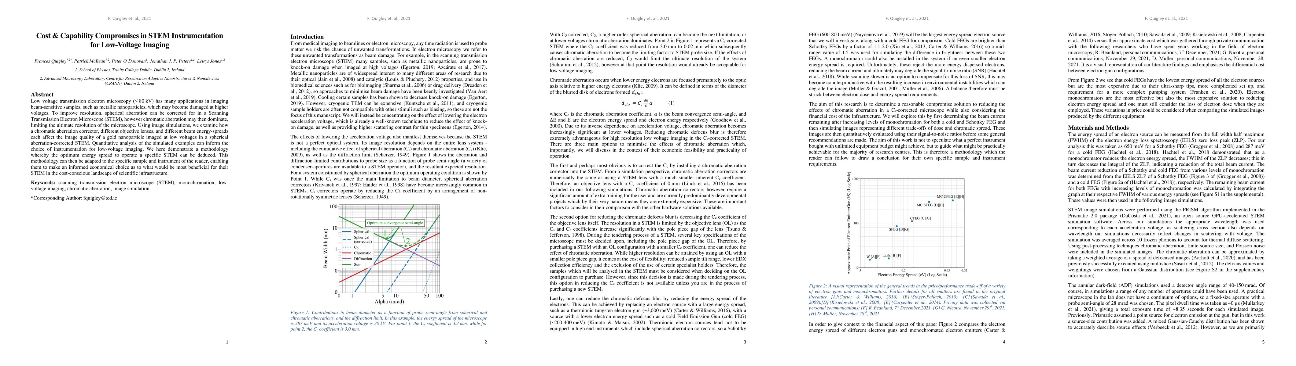
Low voltage transmission electron microscopy (<=80 kV) has many applications in imaging beam-sensitive samples, such as metallic nanoparticles, which may become damaged at higher voltages. To improv...
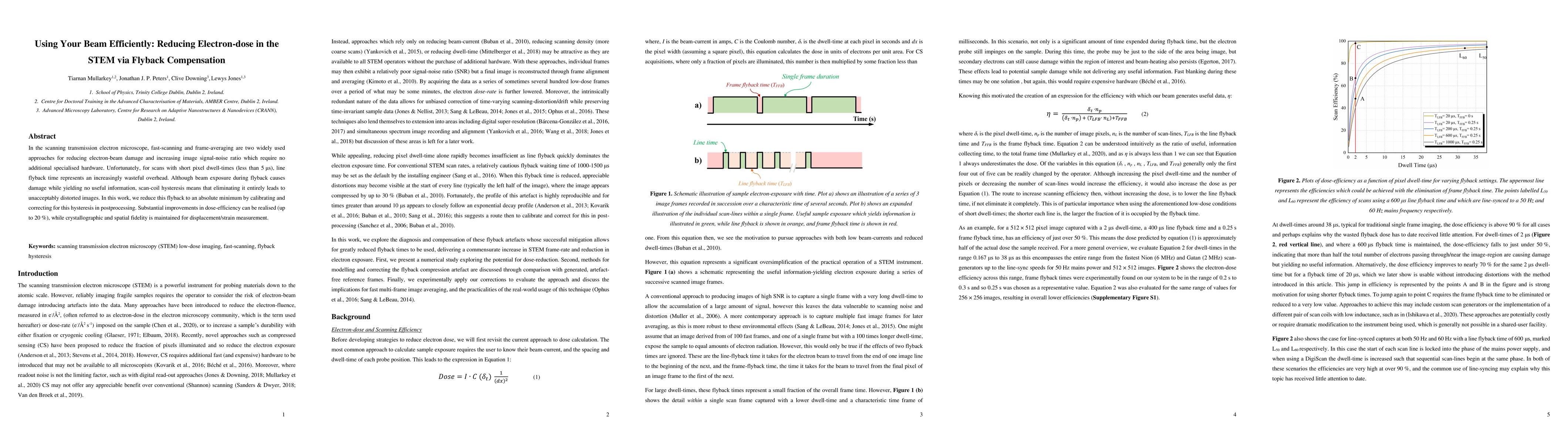
In the scanning transmission electron microscope, fast-scanning and frame-averaging are two widely used approaches for reducing electron-beam damage and increasing image signal-noise ratio which req...
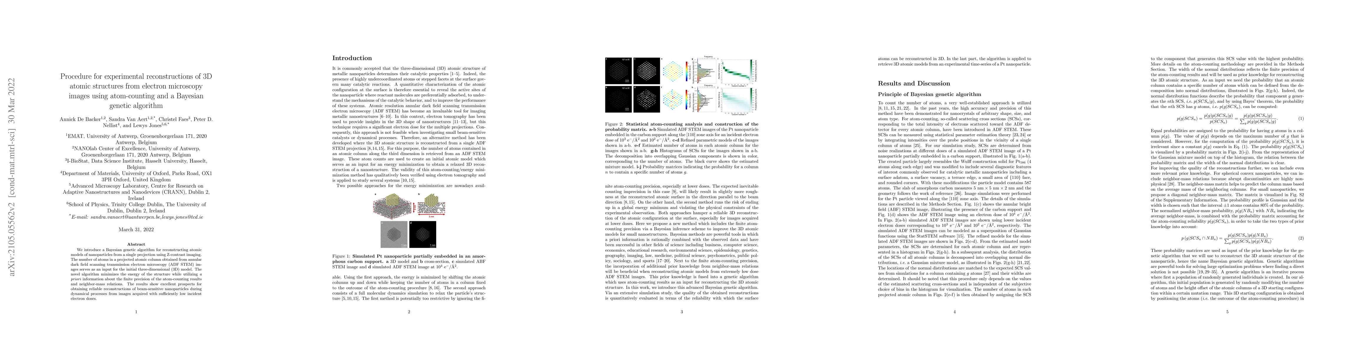
We introduce a Bayesian genetic algorithm for reconstructing atomic models of nanoparticles from a single projection using Z-contrast imaging. The number of atoms in a projected atomic column obtain...
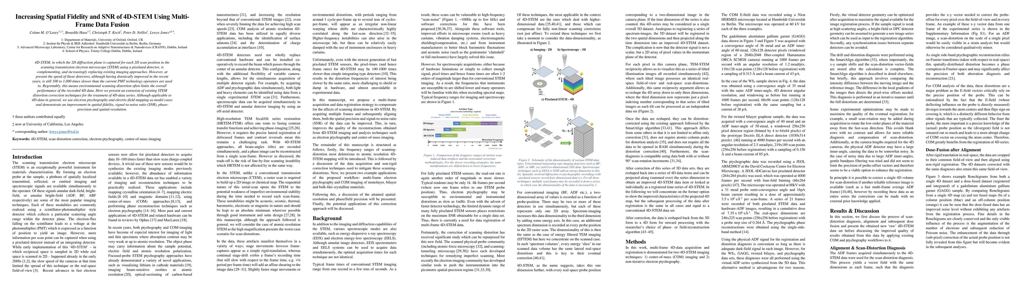
4D-STEM, in which the 2D diffraction plane is captured for each 2D scan position in the scanning transmission electron microscope (STEM) using a pixelated detector, is complementing and increasingly...
The accurate determination of the compositional fluctuations is pivotal in understanding their role in the reduction of efficiency in high indium content $In_{x}Ga_{1-x}N$ light-emitting diodes, the...
When characterising beam-sensitive materials in the scanning transmission electron microscope (STEM), low-dose techniques are essential for the reliable observation of samples in their true state. A...
Tungsten ditelluride is a layered transition metal dichalcogenide (TMD) that has attracted increasing research interest in recent years. WTe2 has demonstrated large non-saturating magnetoresistance,...
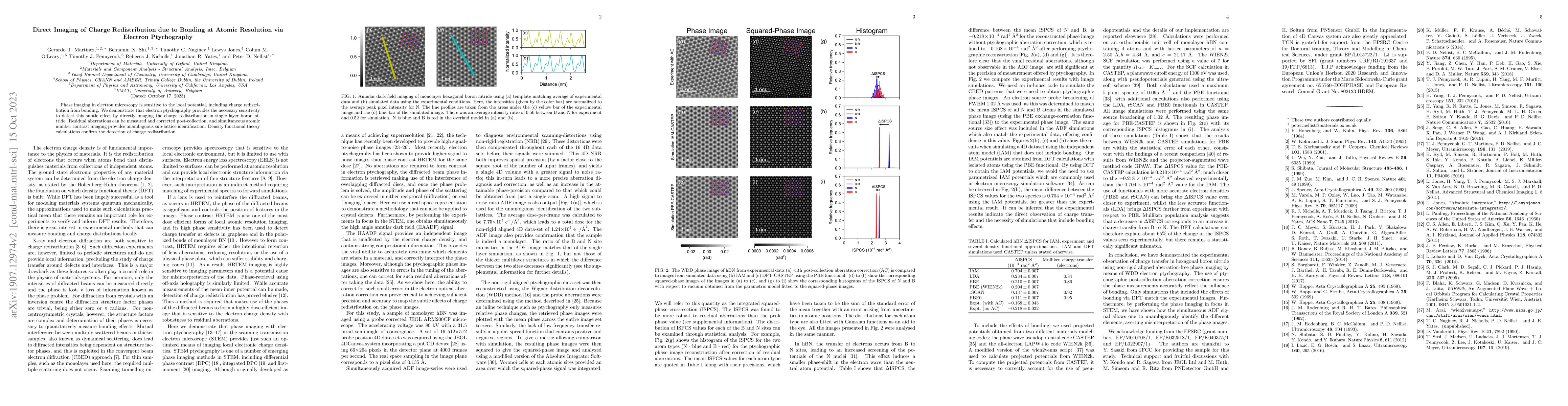
Phase imaging in electron microscopy is sensitive to the local potential, including charge redistribution from bonding. We demonstrate that electron ptychography provides the necessary sensitivity t...
We have investigated the properties of the $\beta$-Ga$_2$O$_3$($\bar201$)/HfO$_2$/Cr/Au MOS (metal-oxide-semiconductor) system after annealing (450$^\circ$C) in different ambient conditions (forming g...
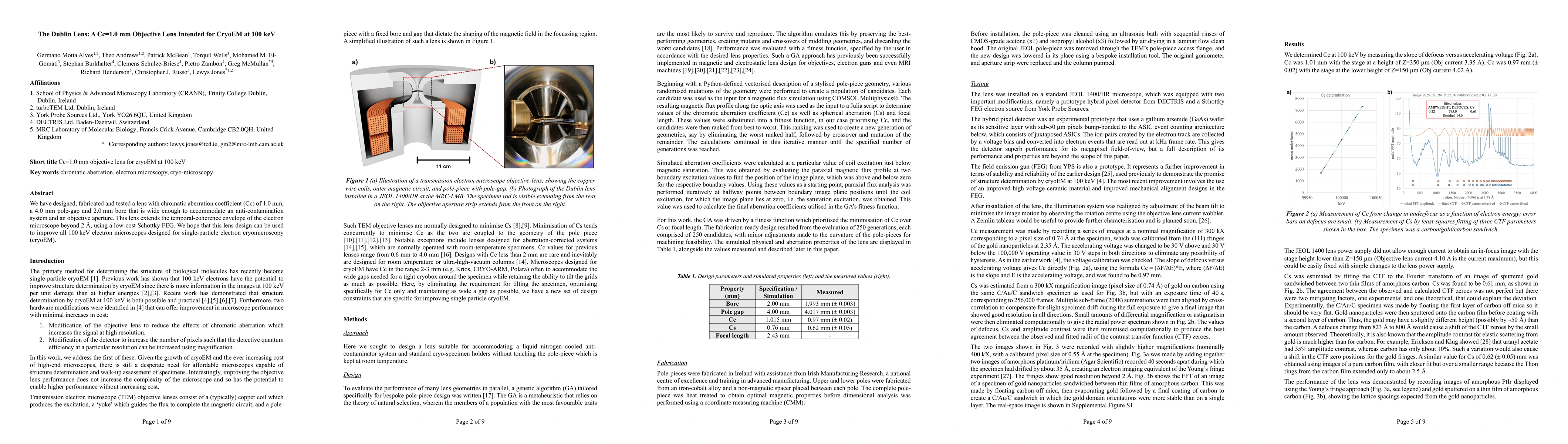
We have designed, fabricated and tested a lens with chromatic aberration coefficient (Cc) of 1.0 mm, a 4.0 mm pole-gap and 2.0 mm bore that is wide enough to accommodate an anti-contamination system a...
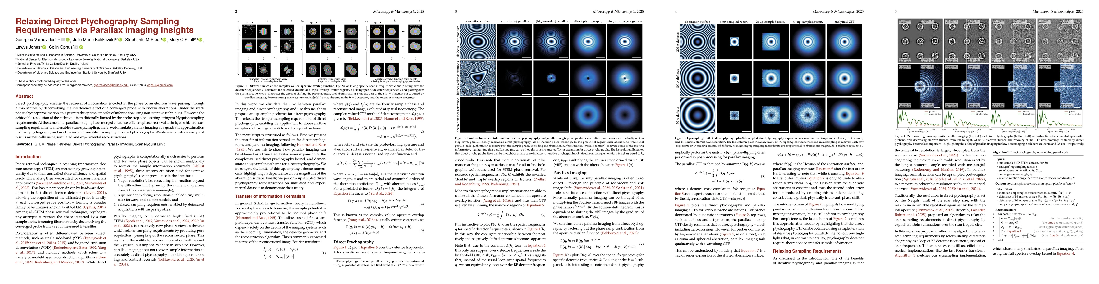
Direct ptychography enables the retrieval of information encoded in the phase of an electron wave passing through a thin sample by deconvolving the interference effect of a converged probe with known ...
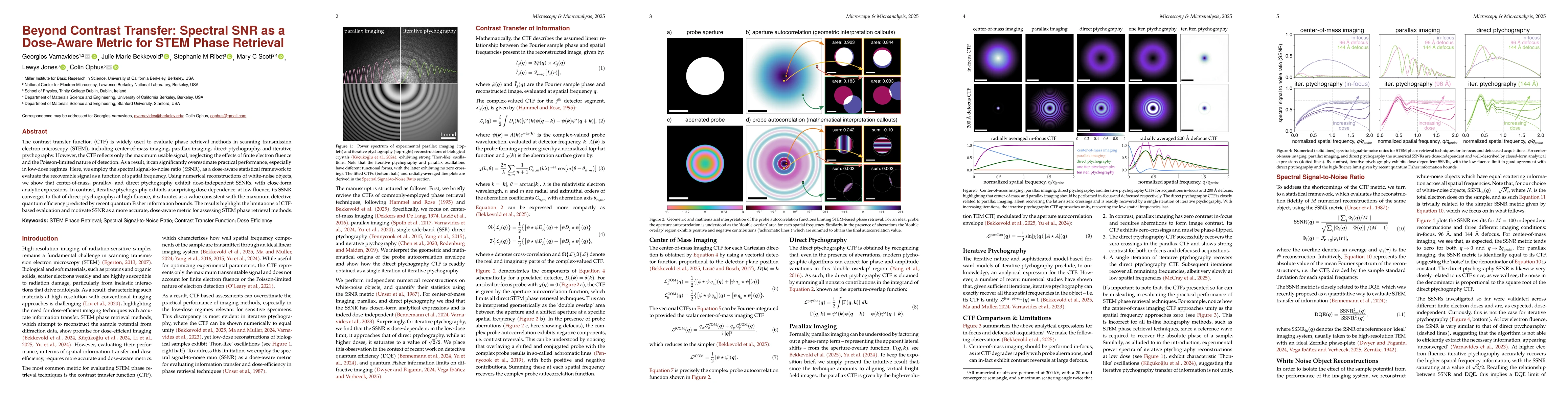
The contrast transfer function (CTF) is widely used to evaluate phase retrieval methods in scanning transmission electron microscopy (STEM), including center-of-mass imaging, parallax imaging, direct ...
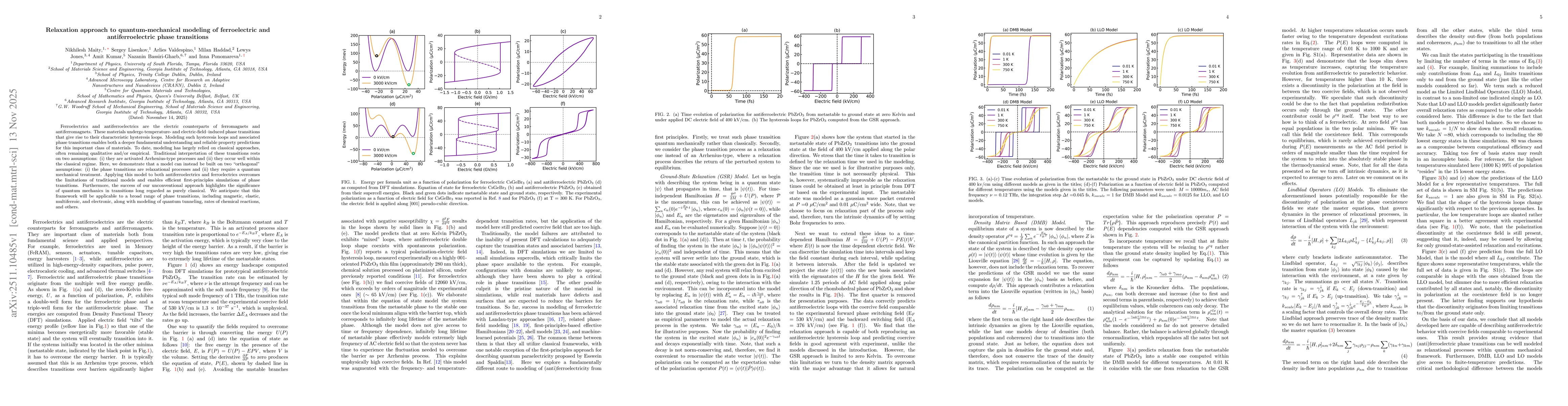
Ferroelectrics and antiferroelectrics are the electric counterparts of ferromagnets and antiferromagnets. These materials undergo temperature- and electric-field-induced phase transitions that give ri...
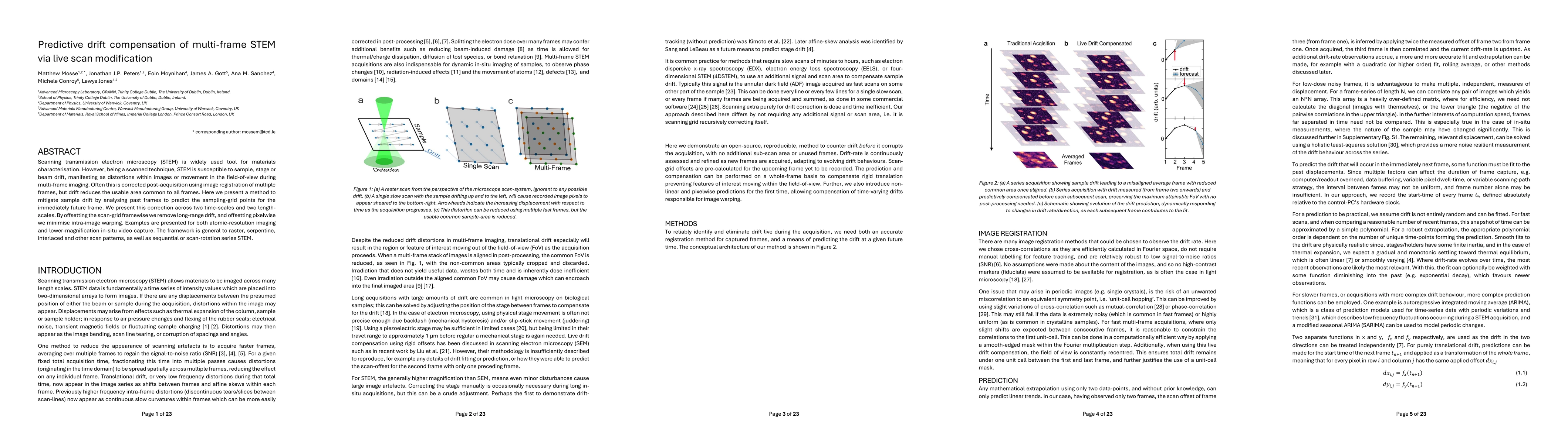
Scanning transmission electron microscopy (STEM) is widely used tool for materials characterisation. However, being a scanned technique, STEM is susceptible to sample, stage or beam drift, manifesting...