Lihong Bao
6 papers on arXiv
Academic Profile
Statistics
Similar Authors
Papers on arXiv
Evidence for Multiferroicity in Single-Layer CuCrSe$_2$
Multiferroic materials, which simultaneously exhibit ferroelectricity and magnetism, have attracted substantial attention due to their fascinating physical properties and potential technological app...
Layer-by-layer growth of bilayer graphene single-crystals enabled by self-transmitting catalytic activity
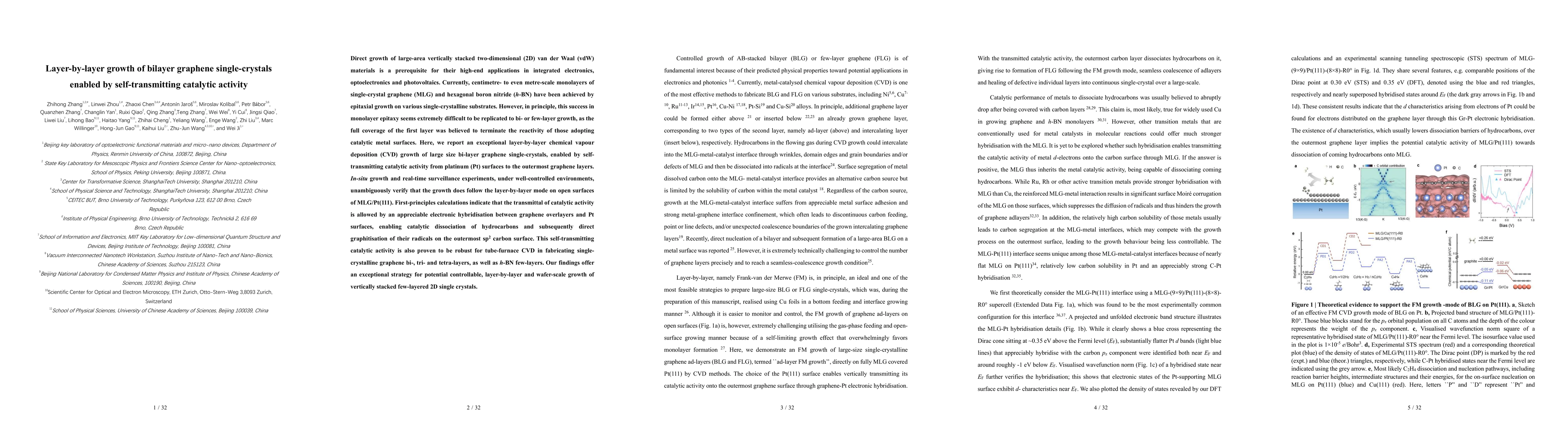
Direct growth of large-area vertically stacked two-dimensional (2D) van der Waal (vdW) materials is a prerequisite for their high-end applications in integrated electronics, optoelectronics and phot...
Atomically sharp interface enabled ultrahigh-speed, nonvolatile memory devices
Development of memory devices with ultimate performance has played a key role in innovation of modern electronics. As a mainstream technology nonvolatile memory devices have manifested high capacity...
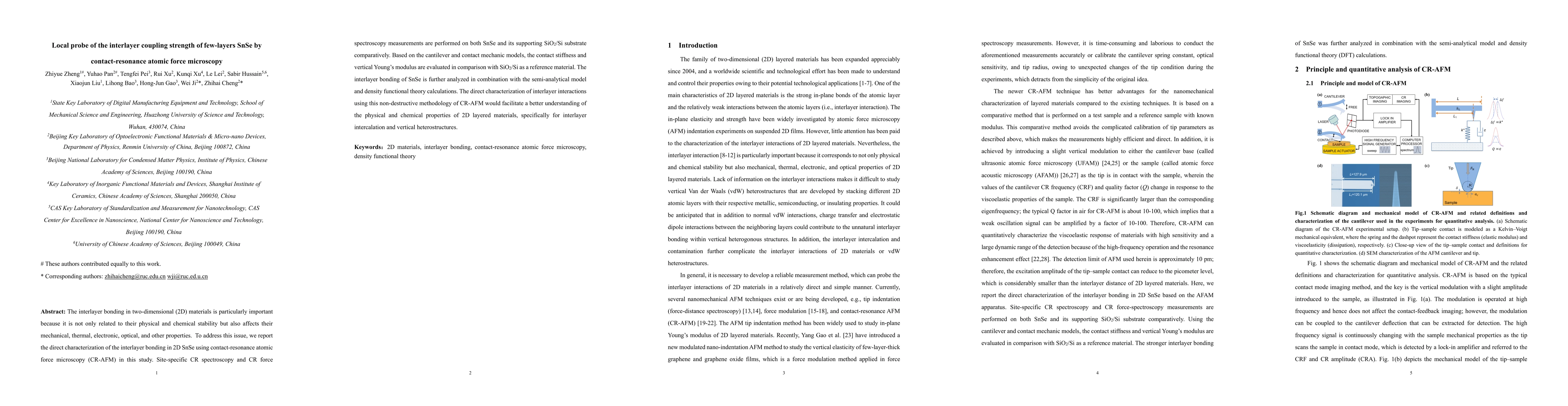
Local probe of the interlayer coupling strength of few-layers SnSe by contact-resonance atomic force microscopy
The interlayer bonding in two dimensional materials is particularly important because it is not only related to their physical and chemical stability but also affects their mechanical, thermal, elec...
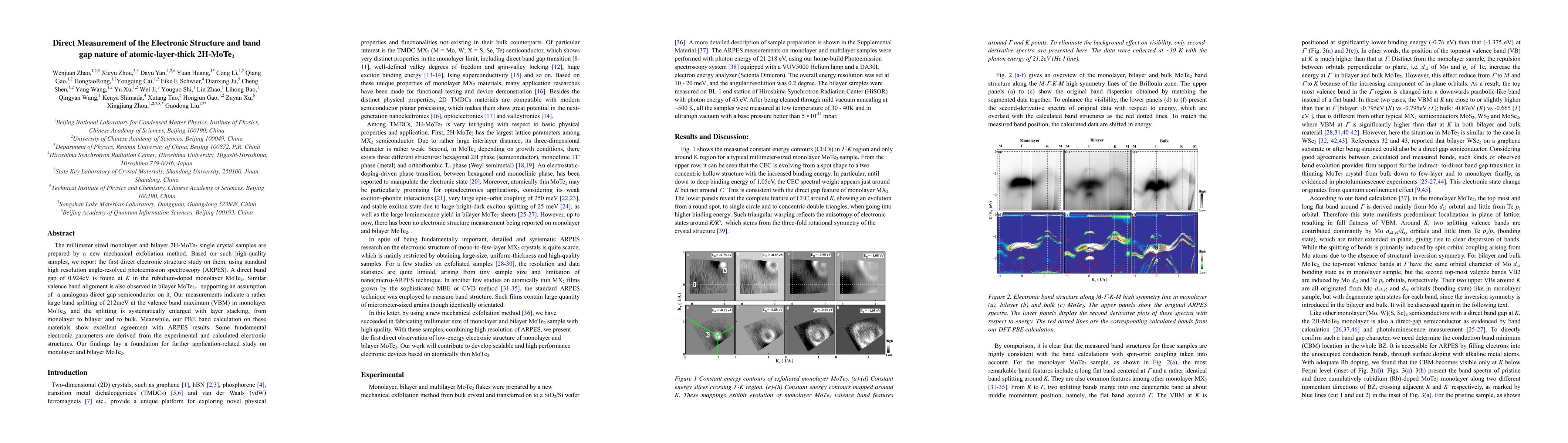
Direct Measurement of the Electronic Structure and band gap nature of atomic-layer-thick 2H-MoTe2
The millimeter sized monolayer and bilayer 2H-MoTe2 single crystal samples are prepared by a new mechanical exfoliation method. Based on such high-quality samples, we report the first direct electro...
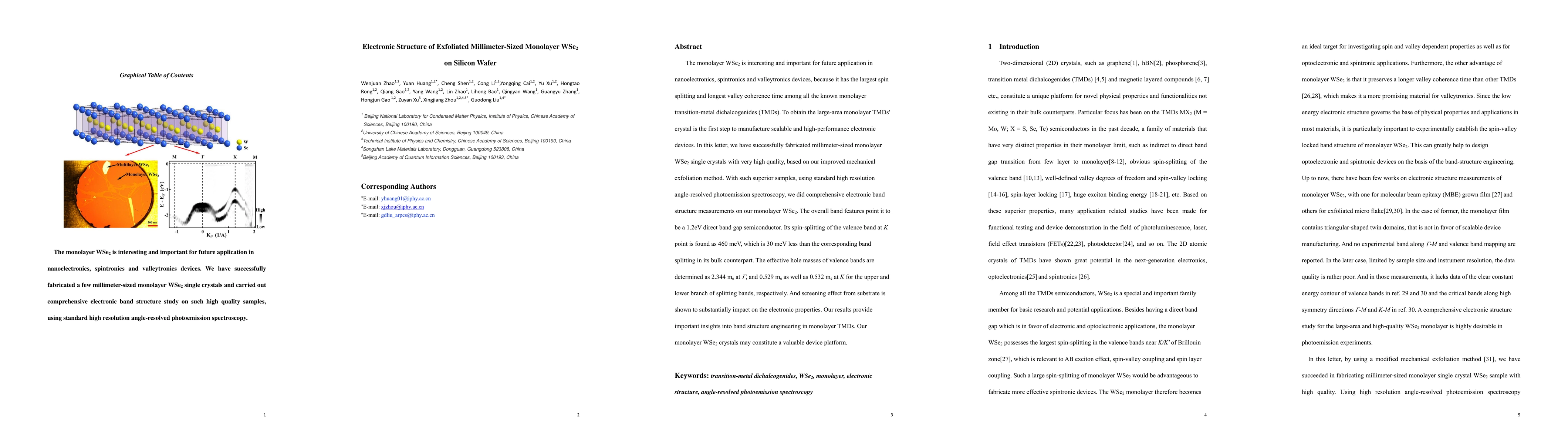
Electronic Structure of Exfoliated Millimeter-Sized Monolayer WSe2 on Silicon Wafer
The monolayer WSe2 is interesting and important for future application in nanoelectronics, spintronics and valleytronics devices, because it has the largest spin splitting and longest valley coheren...