Academic Profile
Statistics
Similar Authors
Papers on arXiv
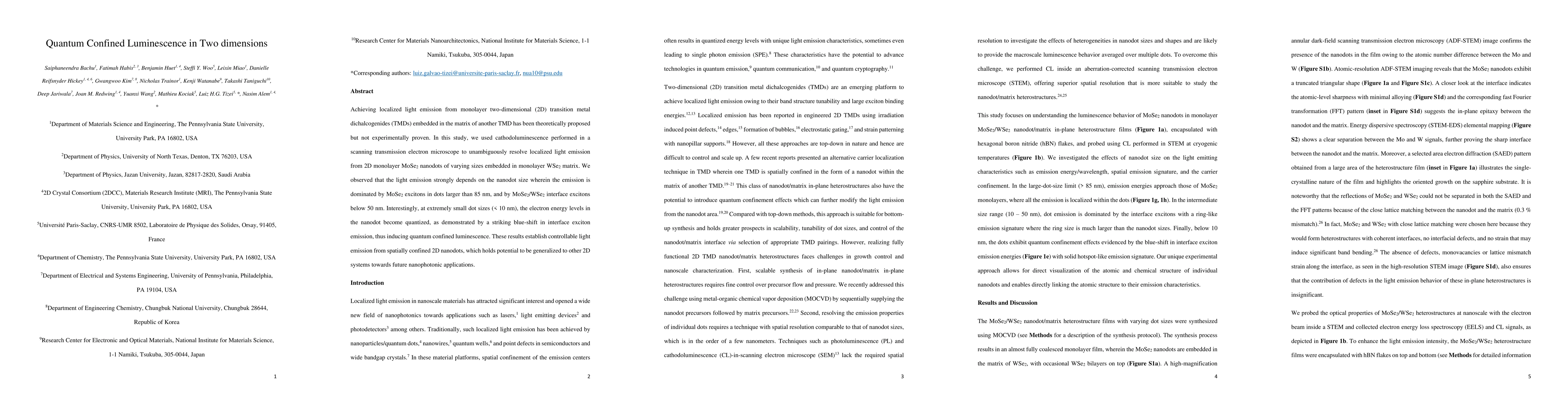
Achieving localized light emission from monolayer two-dimensional (2D) transition metal dichalcogenides (TMDs) embedded in the matrix of another TMD has been theoretically proposed but not experimen...
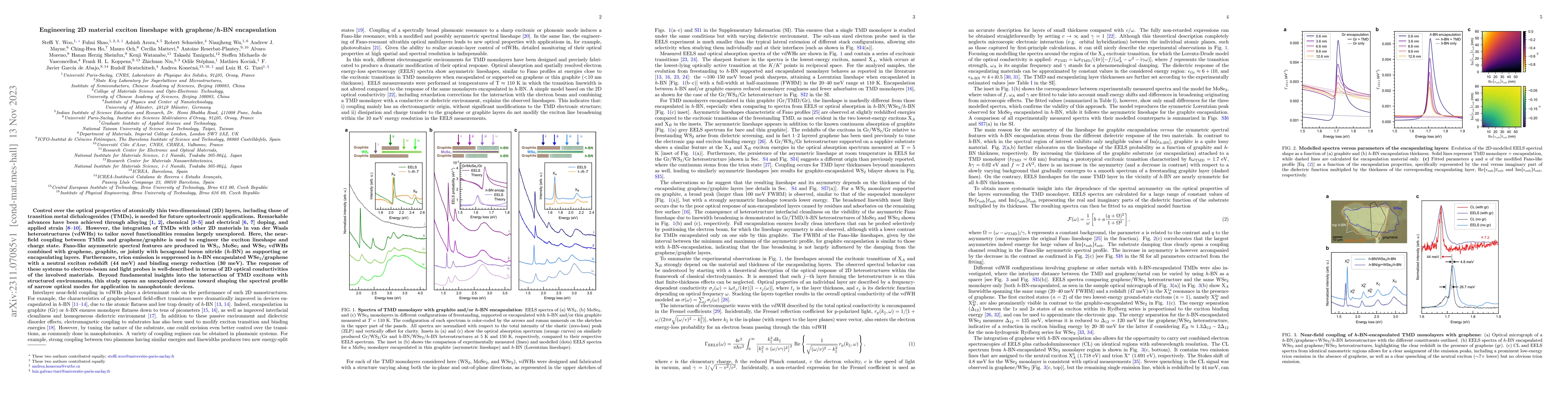
Control over the optical properties of atomically thin two-dimensional (2D) layers, including those of transition metal dichalcogenides (TMDs), is needed for future optoelectronic applications. Rema...
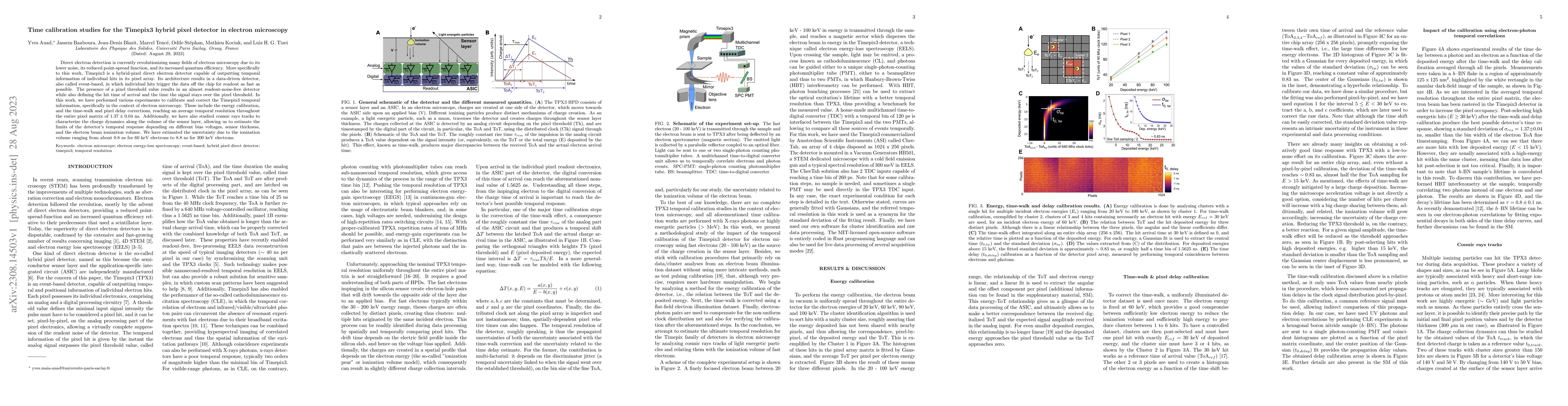
Direct electron detection is currently revolutionizing many fields of electron microscopy due to its lower noise, its reduced point-spread function, and its increased quantum efficiency. More specif...
We report on the design, realization and experimental investigation by spatially resolved monochromated electron energy loss spectroscopy (EELS) of high quality factor cavities with modal volumes sm...
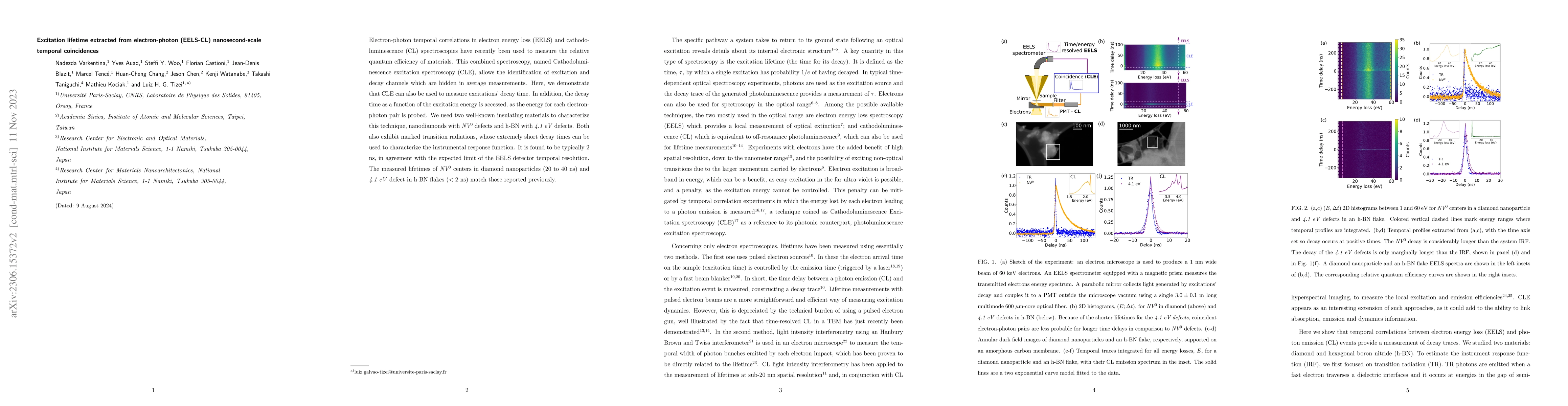
Electron-photon temporal correlations in electron energy loss (EELS) and cathodoluminescence (CL) spectroscopies have recently been used to measure the relative quantum efficiency of materials. This...
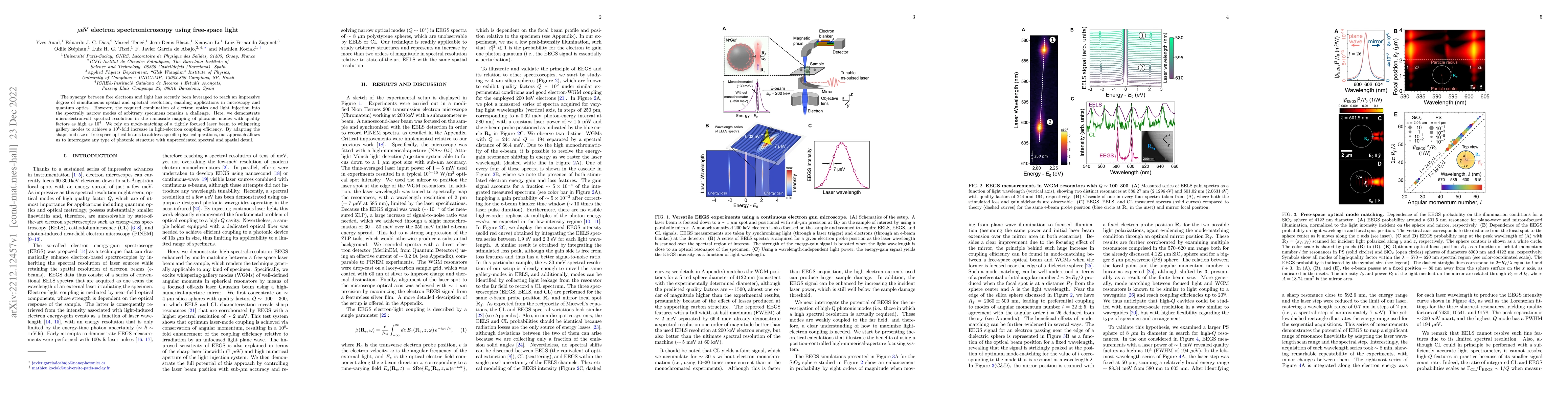
The synergy between free electrons and light has recently been leveraged to reach an impressive degree of simultaneous spatial and spectral resolution, enabling applications in microscopy and quantu...
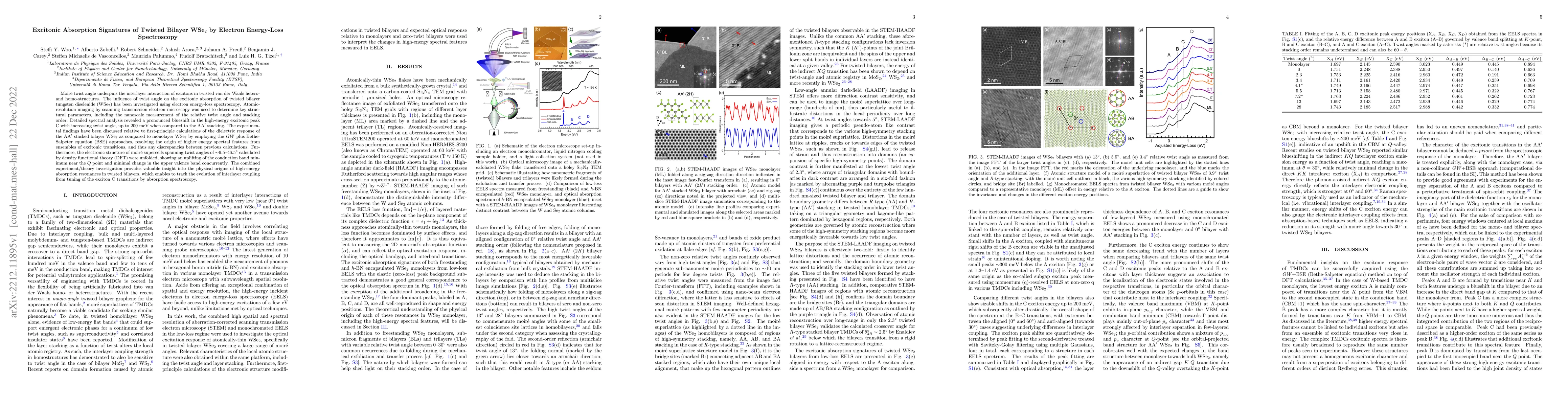
Moir\'{e} twist angle underpins the interlayer interaction of excitons in twisted van der Waals hetero- and homo-structures. The influence of twist angle on the excitonic absorption of twisted bilay...
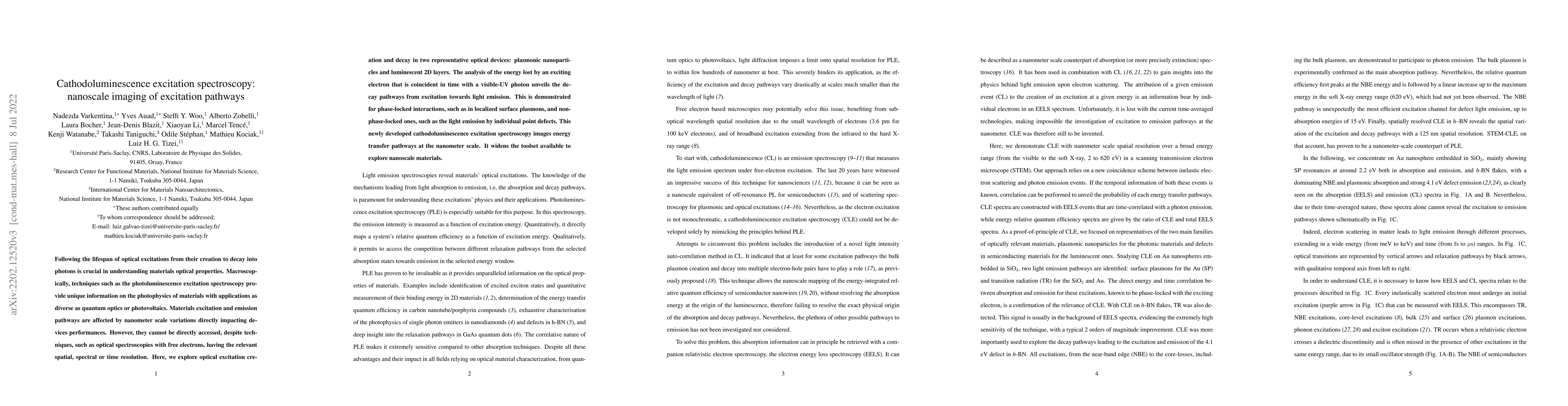
Following the lifespan of optical excitations from their creation to decay into photons is crucial in understanding materials optical properties. Macroscopically, techniques such as the photolumines...
The excitonic states of transition metal dichacolgenide (TMD) monolayers are heavily influenced by their external dielectric environment based on the substrate used. In this work, various wide bandg...
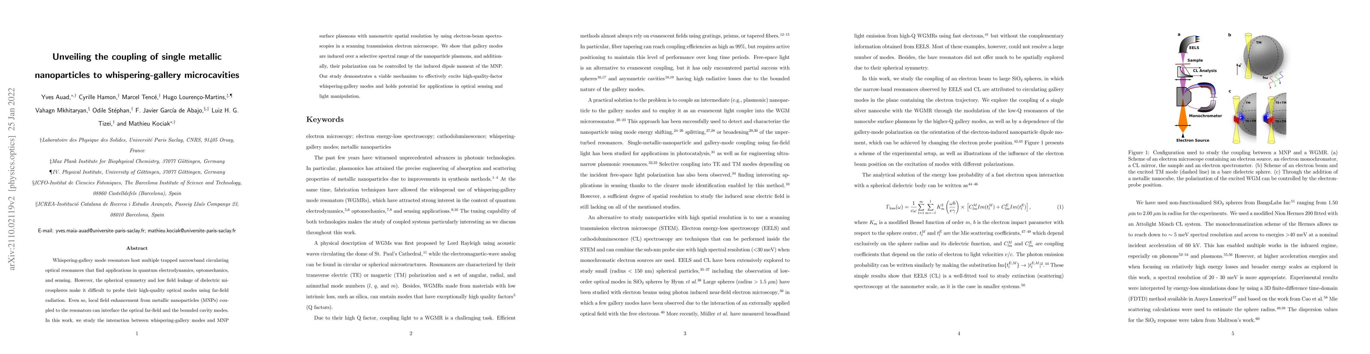
Whispering-gallery mode resonators host multiple trapped narrowband circulating optical resonances that find applications in quantum electrodynamics, optomechanics, and sensing. However, the spheric...
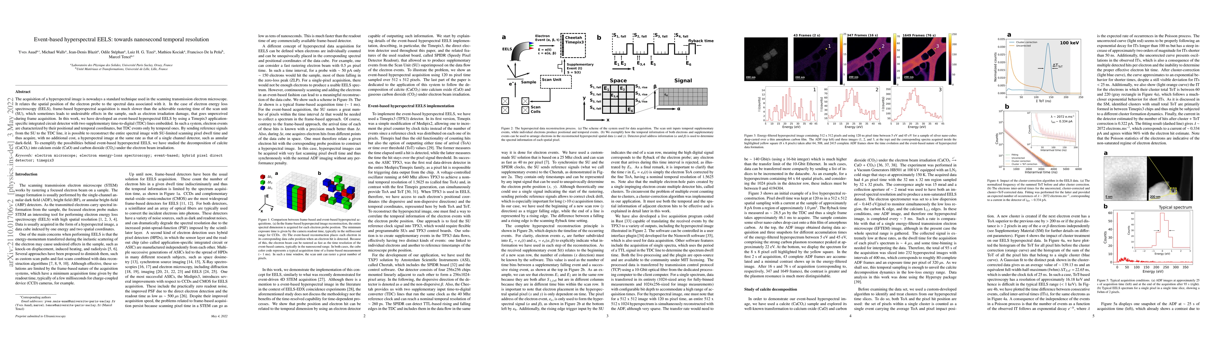
The acquisition of a hyperspectral image is nowadays a standard technique used in the scanning transmission electron microscope. It relates the spatial position of the electron probe to the spectral...
Structural, electronic, and chemical nanoscale modifications of transition metal dichalcogenide monolayers alter their optical properties, including the generation of single photon emitters. A key m...
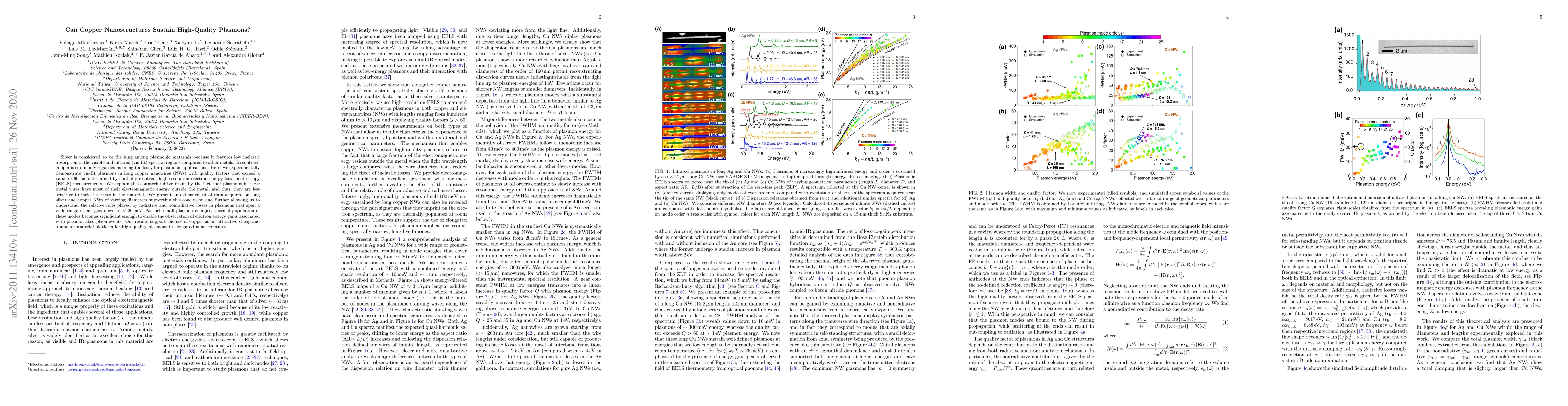
Silver is considered to be the king among plasmonic materials because it features low inelastic absorption in the visible and infrared (vis-IR) spectral regions compared to other metals. In contrast...
The evolution of the scanning modules for scanning transmission electron microscopes (STEM) has realized the possibility to generate arbitrary scan pathways, an approach currently explored to improv...
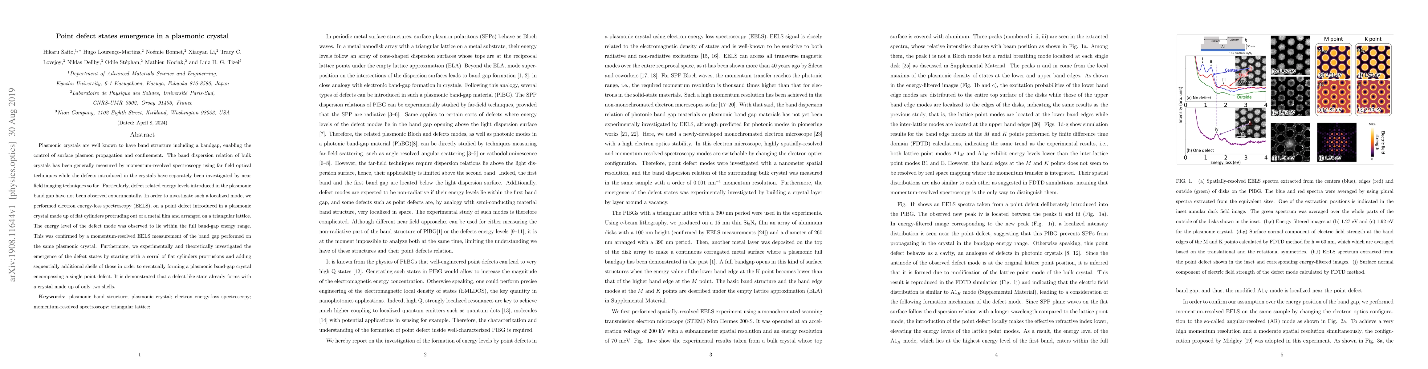
Plasmonic crystals are well known to have band structure including a bandgap, enabling the control of surface plasmon propagation and confinement. The band dispersion relation of bulk crystals has b...
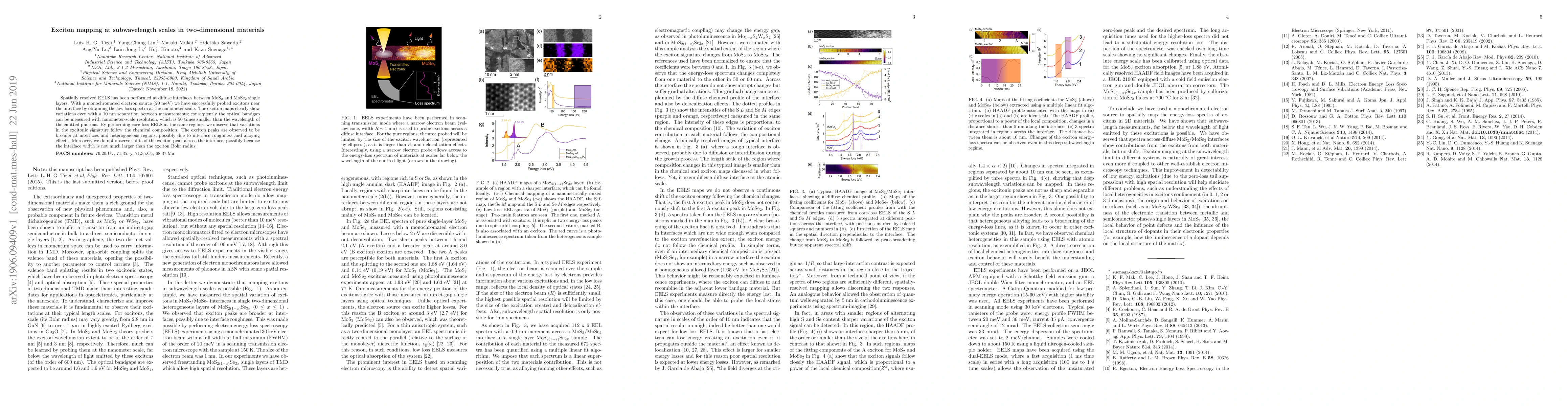
Spatially resolved EELS has been performed at diffuse interfaces between MoS$_2$ and MoSe$_2$ single layers. With a monochromated electron source (20 meV) we have successfully probed excitons near t...
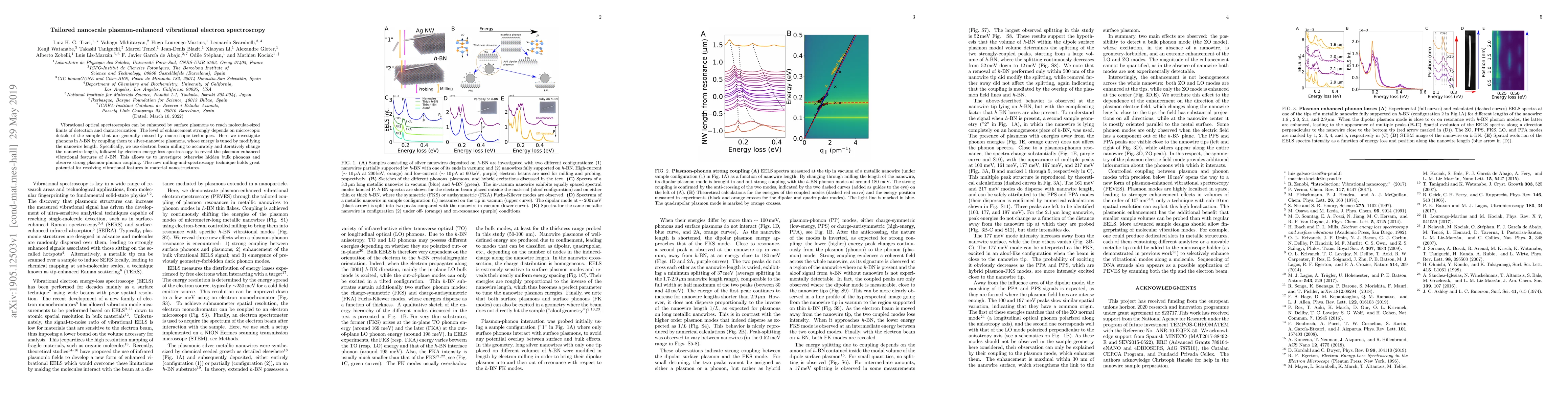
Vibrational optical spectroscopies can be enhanced by surface plasmons to reach molecular-sized limits of detection and characterization. The level of enhancement strongly depends on microscopic det...
Polaritons are compositional light-matter quasiparticles that have recently enabled remarkable breakthroughs in quantum and nonlinear optics, as well as in material science. Despite the enormous pro...
The outstanding properties of transition metal dichalcogenide (TMD) monolayers and their van der Waals (vdW) heterostructures, arising from their structure and the modified electron-hole Coulomb inter...
Thermal transport in nanostructures plays a critical role in modern technologies. As devices shrink, techniques that can measure thermal properties at nanometer and nanosecond scales are increasingly ...
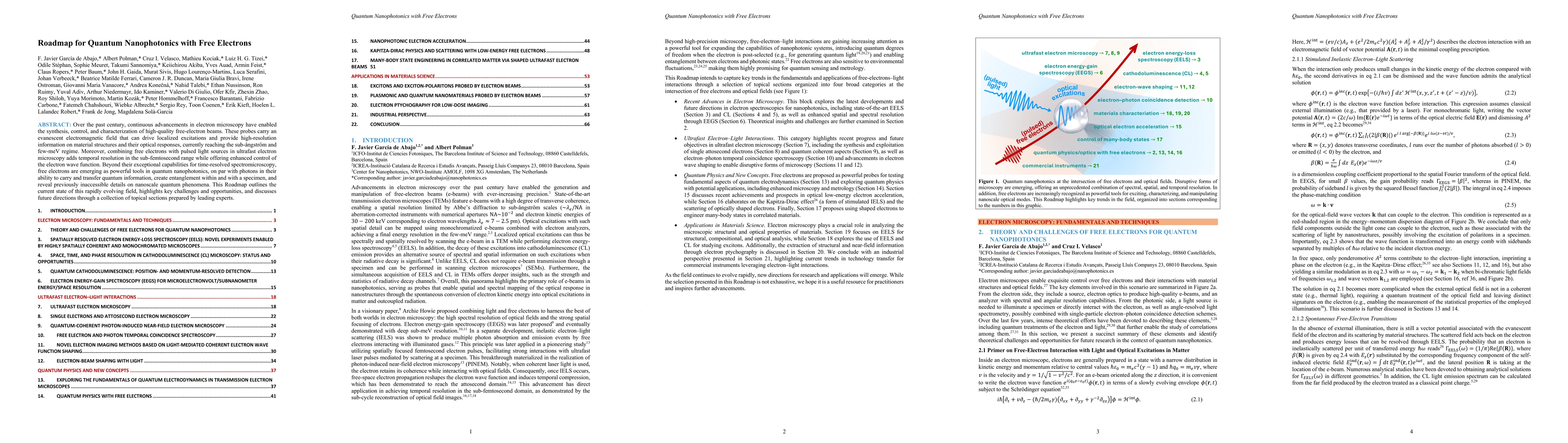
Over the past century, continuous advancements in electron microscopy have enabled the synthesis, control, and characterization of high-quality free-electron beams. These probes carry an evanescent el...
Strong coupling typically occurs between two separate objects or between an object and its environment (such as an atom and a cavity). However, it can also occur between two different excitations with...
Triggered by the development of exfoliation and the identification of a wide range of extraordinary physical properties in self-standing films consisting of one or few atomic layers, two-dimensional (...
Hexagonal-diamond (2H) group IV nanowires are key for advancing group IV-based lasers, quantum electronics, and photonics. Understanding their dielectric response is crucial for performance optimizati...
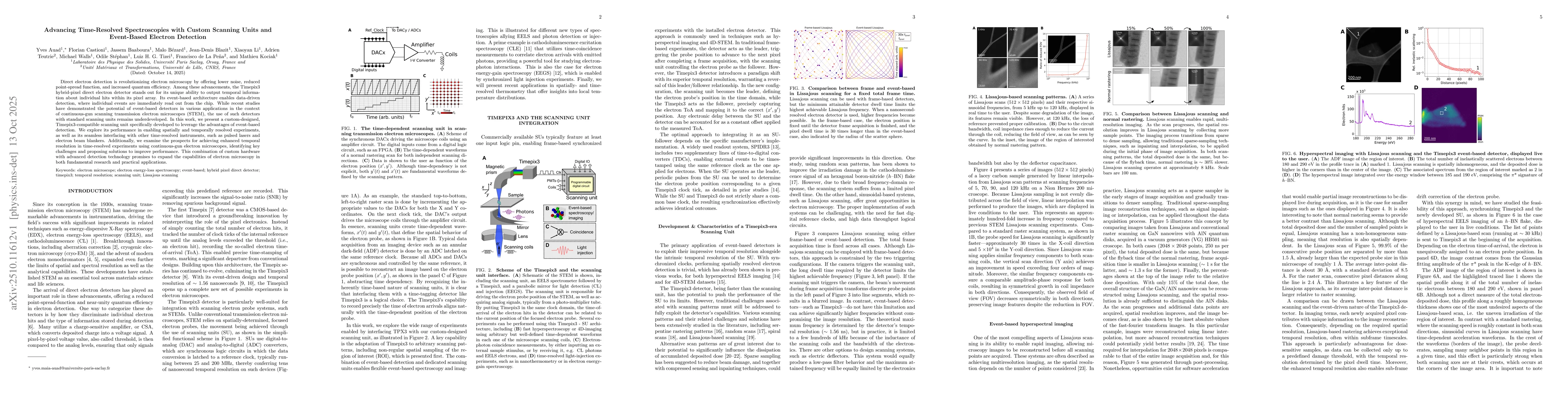
Direct electron detection is revolutionizing electron microscopy by offering lower noise, reduced point-spread function, and increased quantum efficiency. Among these advancements, the Timepix3 hybrid...
There is a growing interest in identifying the origin of single-photon emission in hexagonal boron nitride (hBN), with proposed candidates including boron and nitrogen vacancies as well as carbon subs...
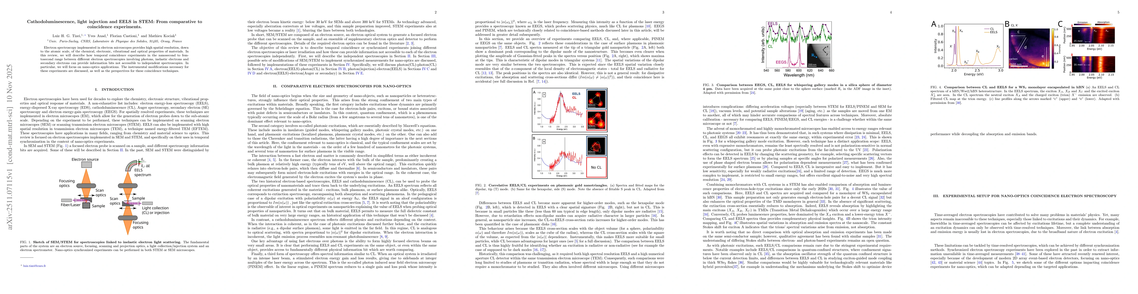
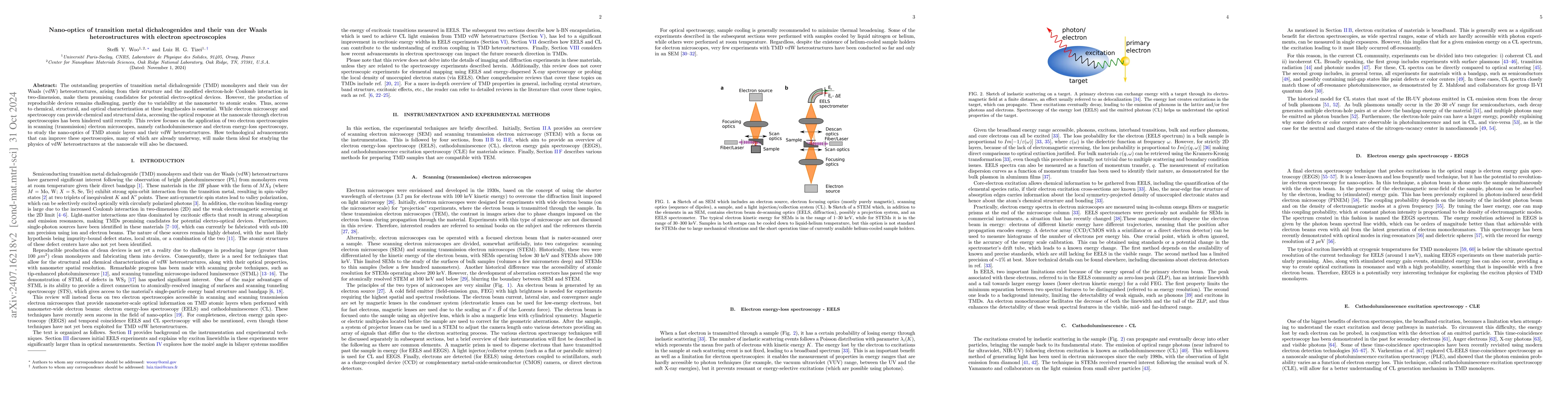
Electron spectroscopy implemented in electron microscopes provides high spatial resolution, down to the atomic scale, of the chemical, electronic, vibrational and optical properties of materials. In t...
Integrated opto-electronic devices have the potential to revolutionize information processing, with substantial increase in compute speed, seamless information transfer and reduction of energy consump...