Academic Profile
Statistics
Similar Authors
Papers on arXiv
Organic electro-optic (OEO) materials have demonstrated promising performance in developing electro-optic phase shifters (EOPS) and modulators compared to their inorganic counterparts. Integration w...
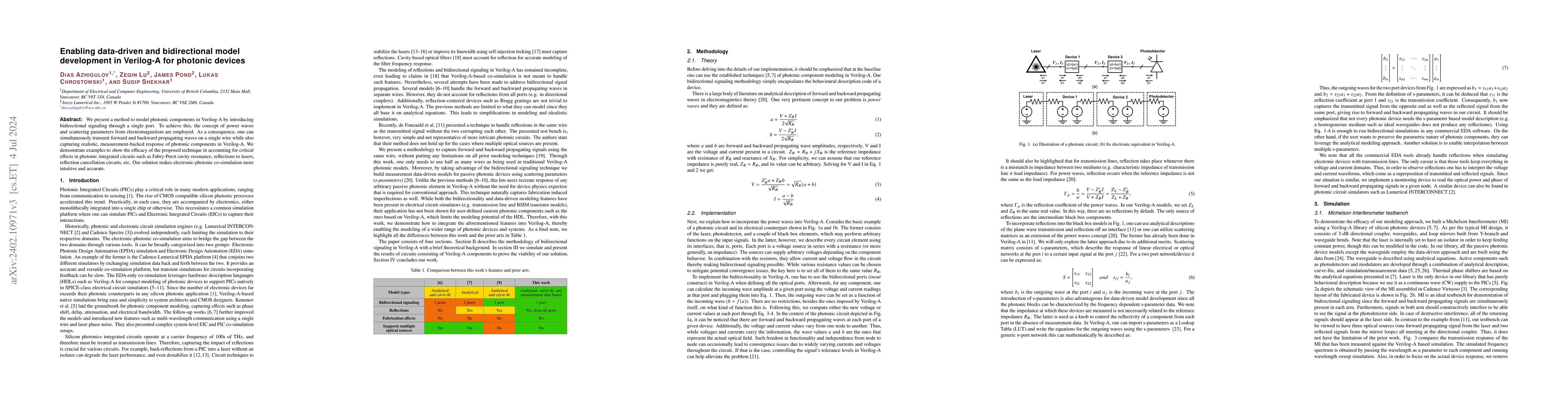
We present a method to model photonic components in Verilog-A by introducing bidirectional signaling through a single port. To achieve this, the concept of power waves and scattering parameters from...
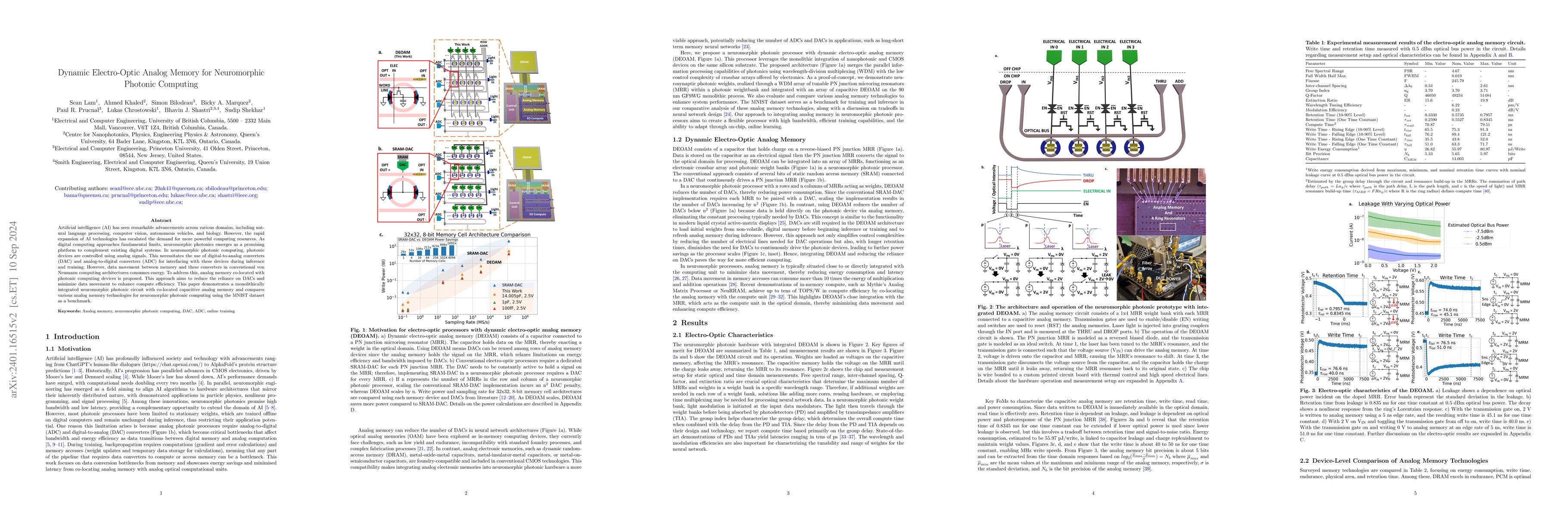
Artificial intelligence (AI) has seen remarkable advancements across various domains, including natural language processing, computer vision, autonomous vehicles, and biology. However, the rapid exp...
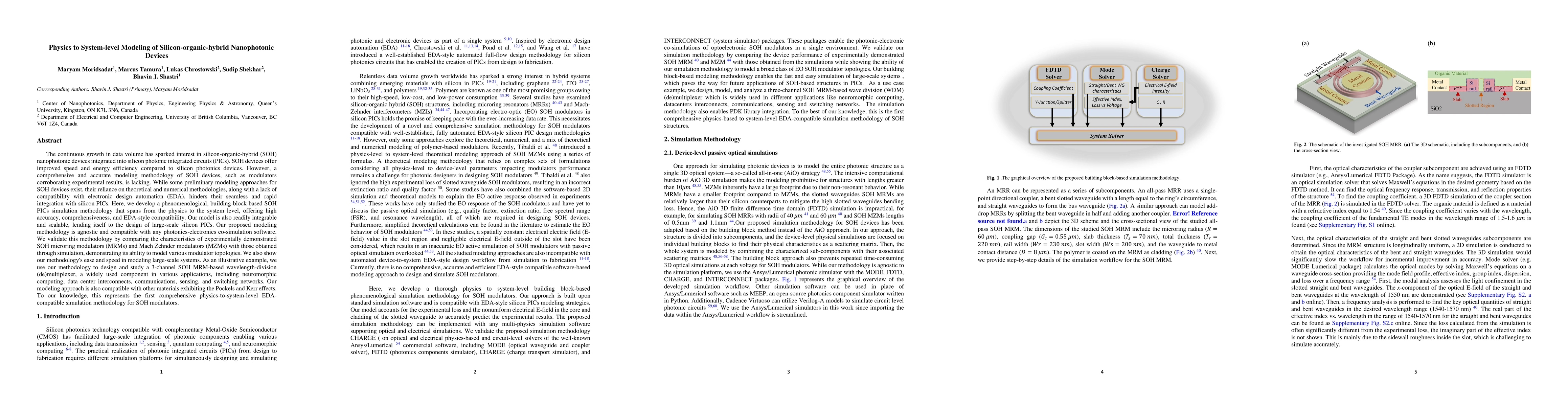
The continuous growth in data volume has sparked interest in silicon-organic-hybrid nanophotonic devices integrated into silicon photonic integrated circuits (PICs). SOH devices offer improved speed...
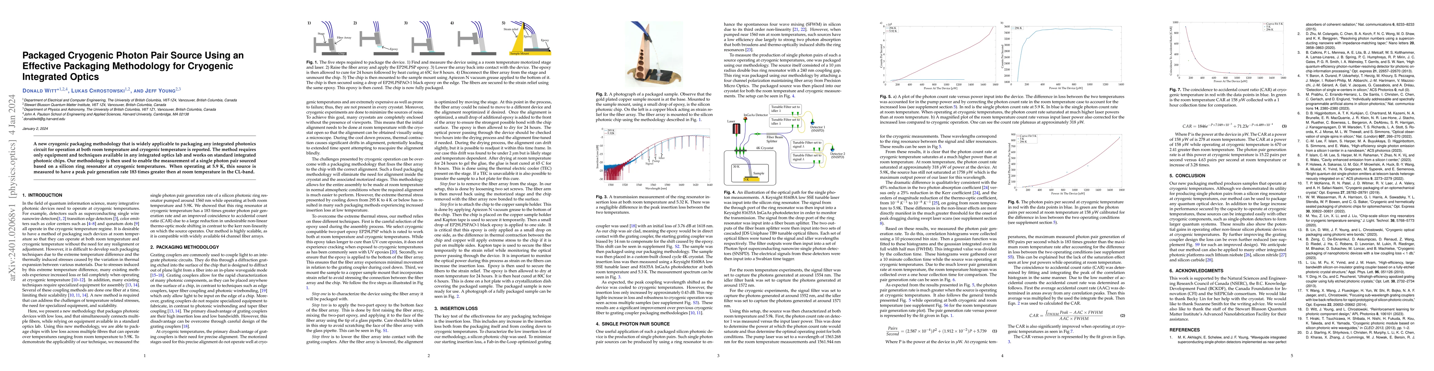
A new cryogenic packaging methodology that is widely applicable to packaging any integrated photonics circuit for operation at both room temperature and cryogenic temperature is reported. The method...
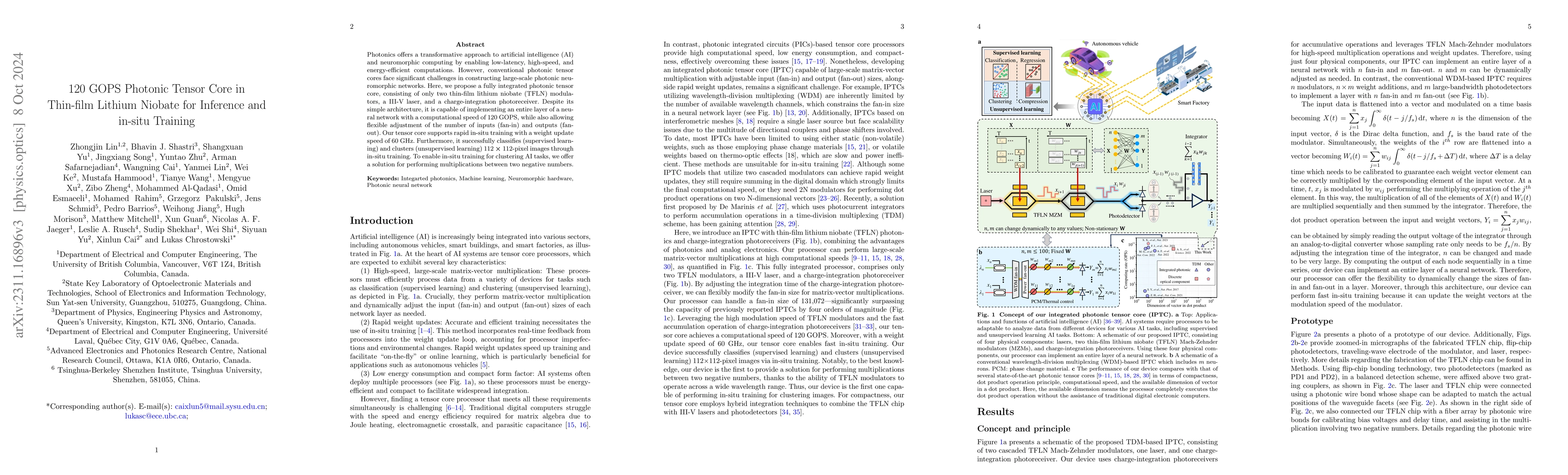
Photonics offers a transformative approach to artificial intelligence (AI) and neuromorphic computing by providing low latency, high bandwidth, and energy-efficient computations. Here, we introduce ...
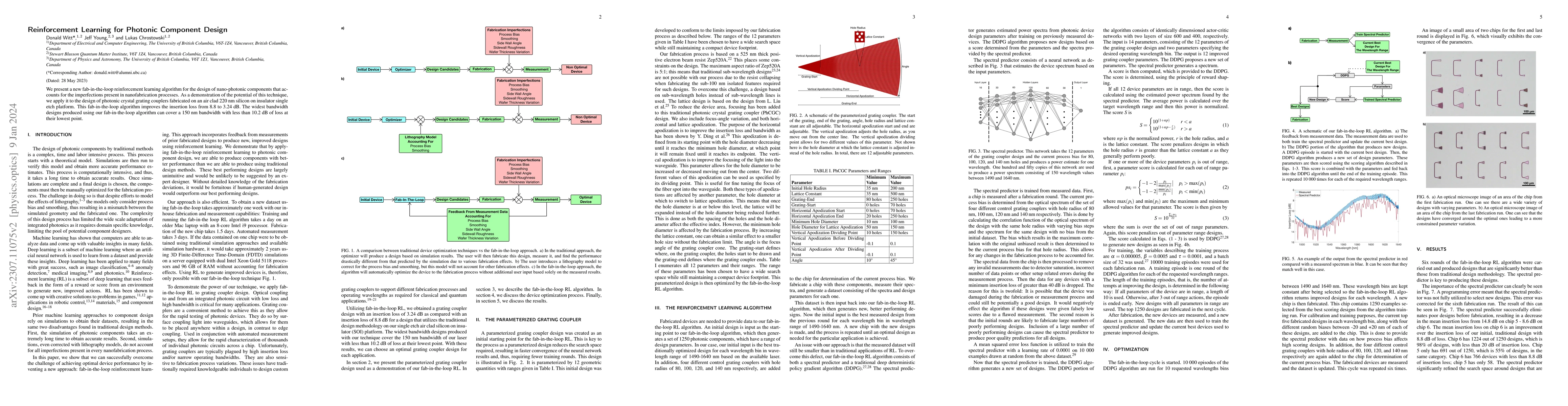
We present a new fab-in-the-loop reinforcement learning algorithm for the design of nano-photonic components that accounts for the imperfections present in nanofabrication processes. As a demonstrat...
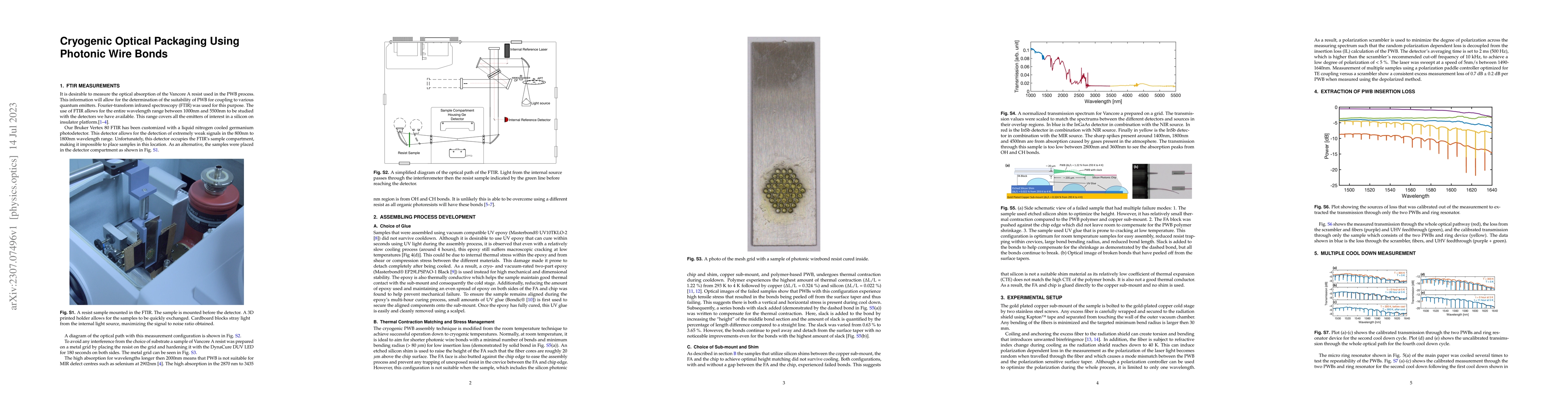
We present the required techniques for the successful low loss packaging of integrated photonic devices capable of operating down to 970 mK utilizing photonic wire bonds. This scalable technique is ...
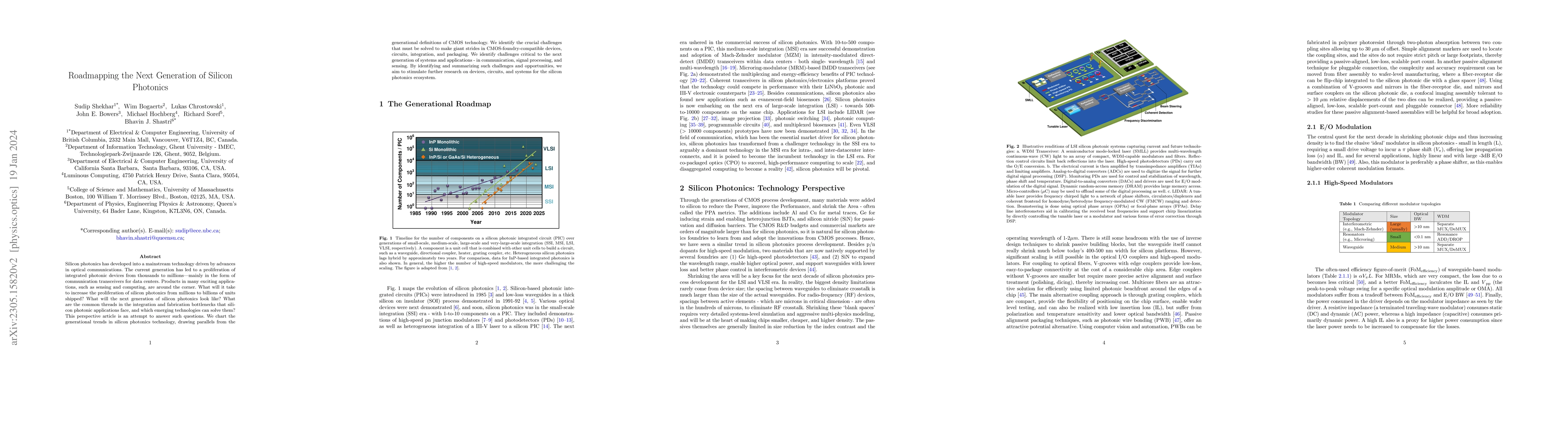
Silicon photonics has developed into a mainstream technology driven by advances in optical communications. The current generation has led to a proliferation of integrated photonic devices from thous...
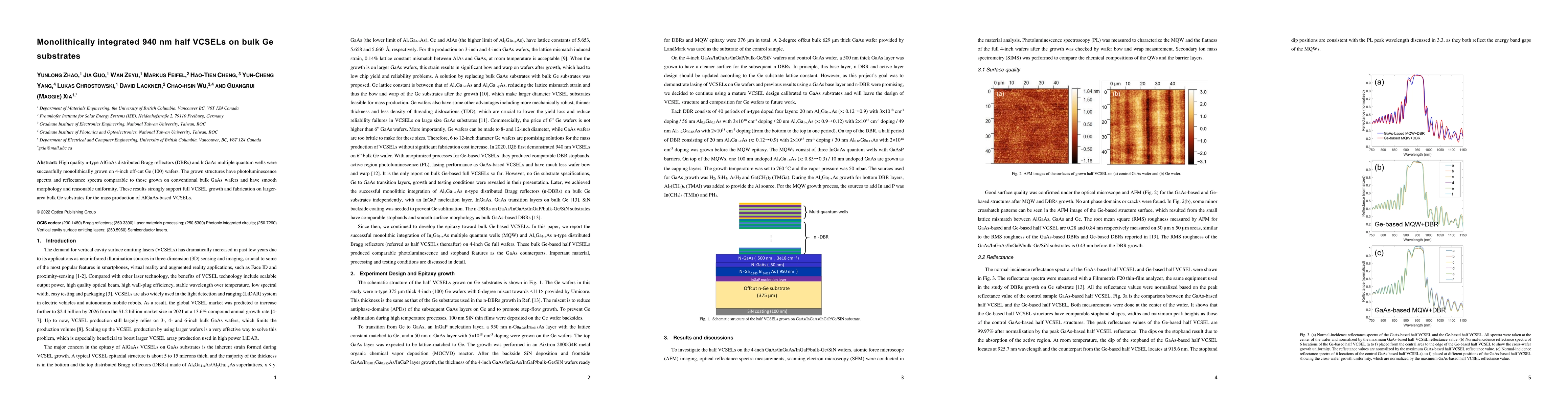
High quality n-type AlGaAs distributed Bragg reflectors (DBRs) and lnGaAs multiple quantum wells were successfully monolithically grown on 4-inch off-cut Ge (100) wafers. The grown structures have p...
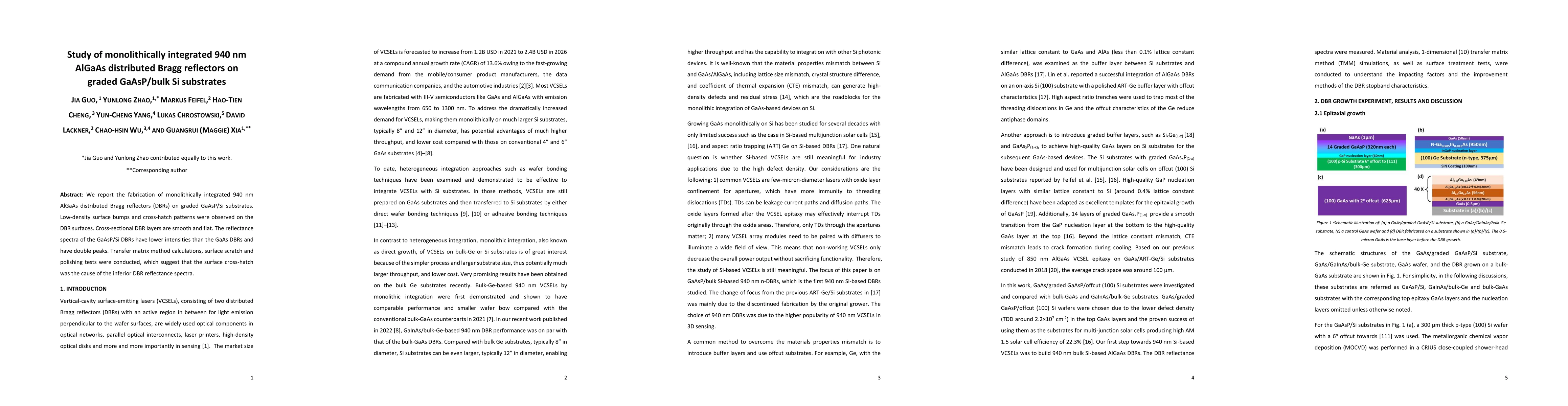
We report the fabrication of monolithically integrated 940 nm AlGaAs distributed Bragg reflectors (DBRs) on graded GaAsP/Si substrates. Low-density surface bumps and cross-hatch patterns were observ...
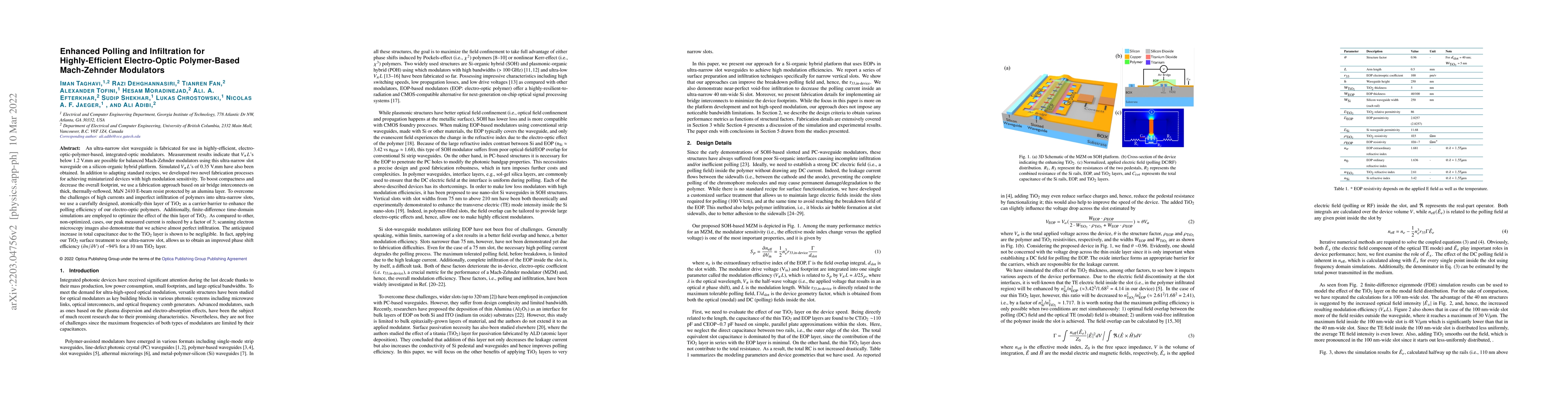
An ultra-narrow slot waveguide is fabricated for use in highly-efficient, electro-optic-polymer-based, integrated-optic modulators. Measurement results indicate that $V_\pi L$'s below 1.2 V.mm are p...
High quality 940 nm Al$_x$Ga$_{1-x}$As n-type distributed Bragg reflectors (DBRs) were successfully monolithically grown on off-cut Ge (100) substrates. The Ge-DBRs have reflectivity spectra compara...
Neural networks have enabled applications in artificial intelligence through machine learning, and neuromorphic computing. Software implementations of neural networks on conventional computers that ...
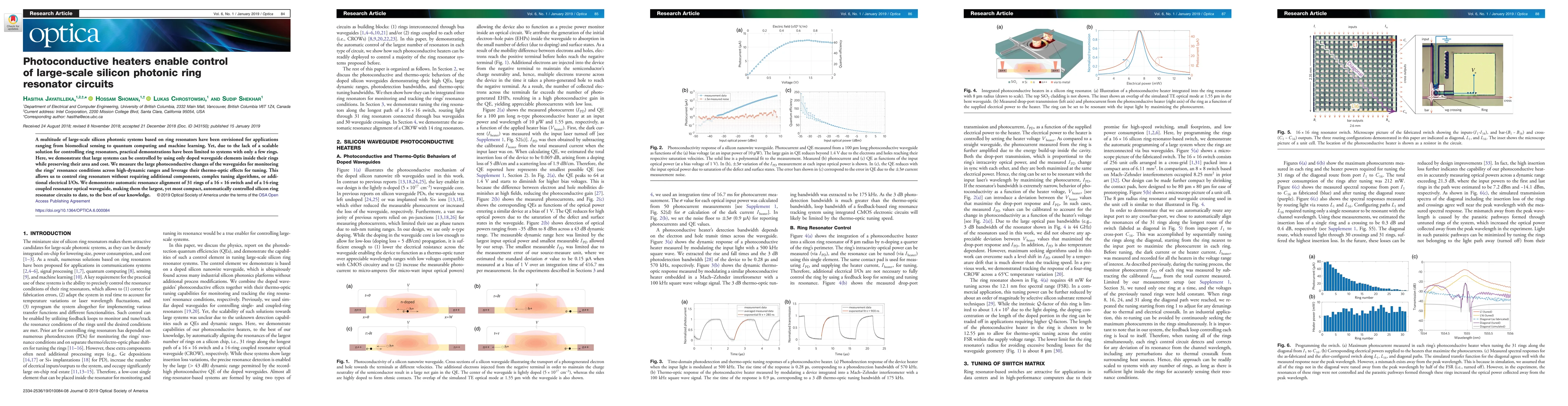
A multitude of large-scale silicon photonic systems based on ring resonators have been envisioned for applications ranging from biomedical sensing to quantum computing and machine learning. Yet, due...
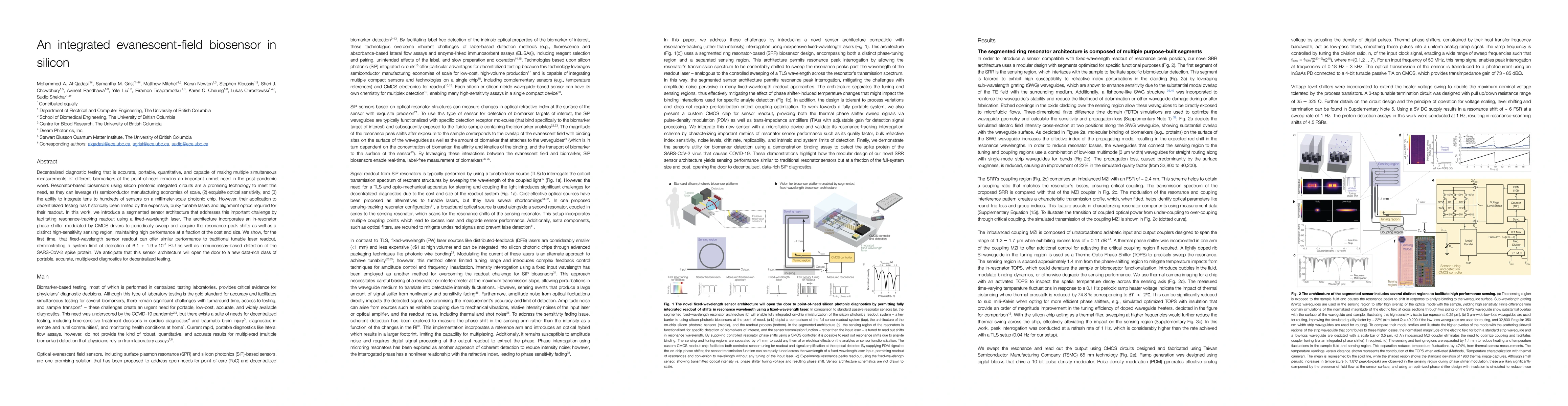
Decentralized diagnostic testing that is accurate, portable, quantitative, and capable of making multiple simultaneous measurements of different biomarkers at the point-of-need remains an important un...
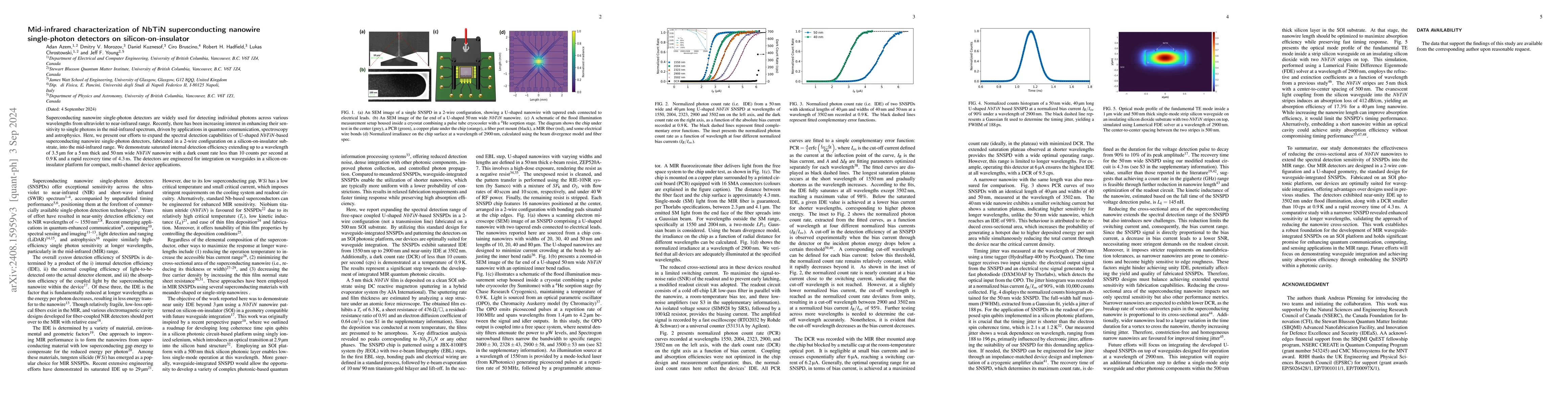
Superconducting nanowire single-photon detectors are widely used for detecting individual photons across various wavelengths from ultraviolet to near-infrared range. Recently, there has been increasin...
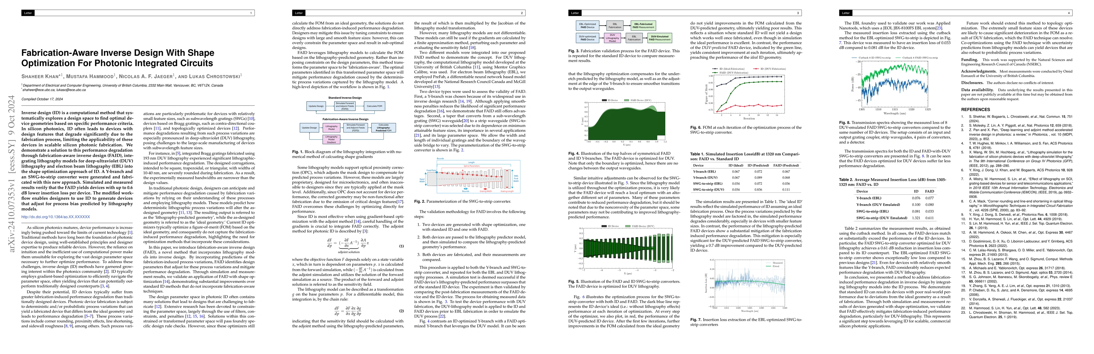
Inverse design (ID) is a computational method that systematically explores a design space to find optimal device geometries based on specific performance criteria. In silicon photonics, ID often leads...
This roadmap consolidates recent advances while exploring emerging applications, reflecting the remarkable diversity of hardware platforms, neuromorphic concepts, and implementation philosophies repor...
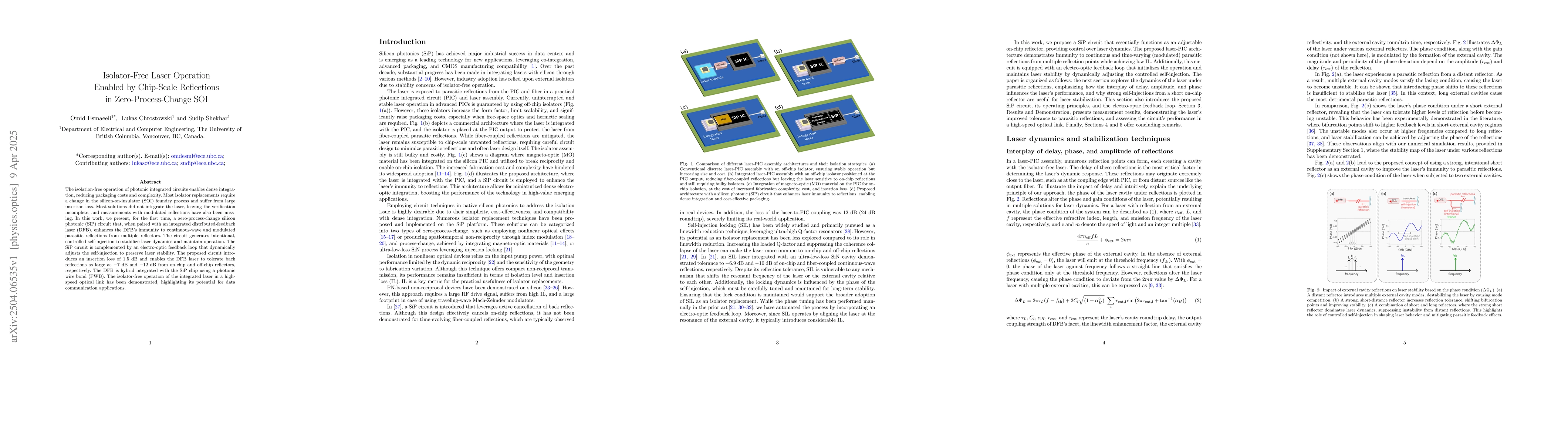
The isolation-free operation of photonic integrated circuits enables dense integration, reducing packaging costs and complexity. Most isolator replacements require a change in the silicon-on-insulator...
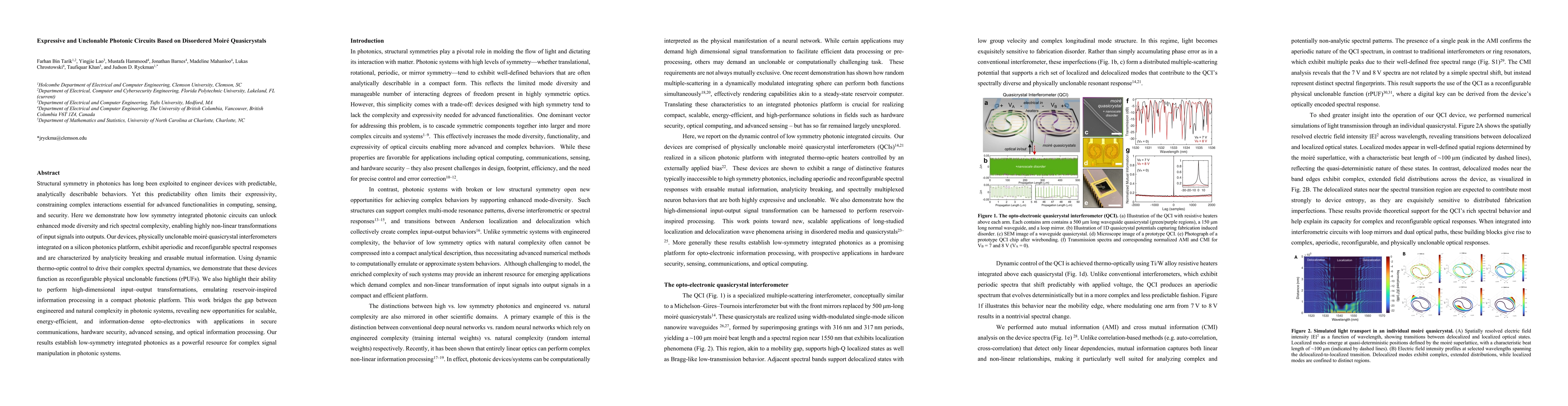
Structural symmetry in photonics has long been exploited to engineer devices with predictable, analytically describable behaviors. Yet this predictability often limits their expressivity, constraining...
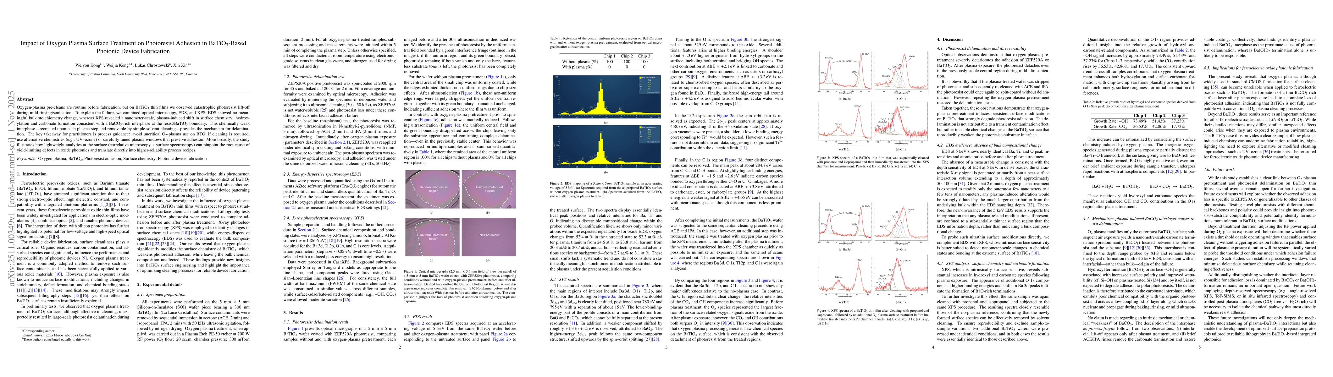
Oxygen-plasma pre-cleans are routine before fabrication, but on BaTiO3 thin films we observed catastrophic photoresist lift-off during mild rinsing and sonication. To explain the failure, we combined ...
Silicon-organic hybrid (SOH) platforms exhibit exceptional electro-optic (EO) properties, including high-speed operation, low energy consumption, and compact footprints. However, the absence of a scal...