ArxivLens
L
Researcher

Lutz Waldecker

16 papers on arXiv

16 arXiv Papers
49 Total Publications
Profile

Academic Profile

Name L. Waldecker
Total Papers 49
Scholar Profile View on Semantic Scholar
Metrics

Statistics

16 arXiv Papers
49 Total Publications
Publications

Papers on arXiv

Thumbnail for Negative electronic compressibility in charge islands in twisted bilayer
  graphene
arXiv
Negative electronic compressibility in charge islands in twisted bilayer graphene

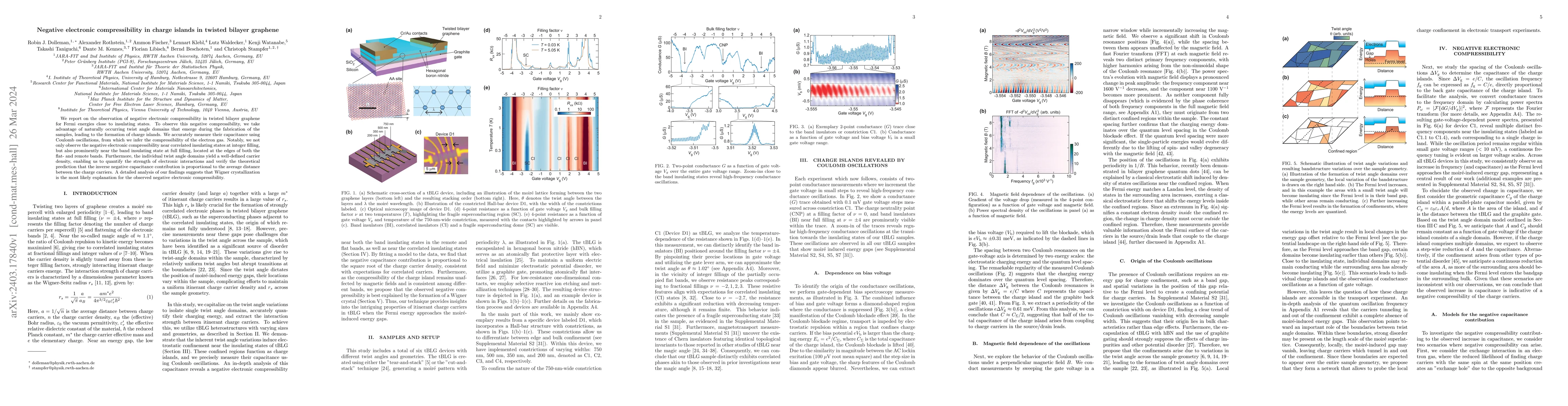
We report on the observation of negative electronic compressibility in twisted bilayer graphene for Fermi energies close to insulating states. To observe this negative compressibility, we take advan...

Thumbnail for Distance dependence of the energy transfer mechanism in WS$_2$-graphene
  heterostructures
arXiv
Distance dependence of the energy transfer mechanism in WS$_2$-graphene heterostructures

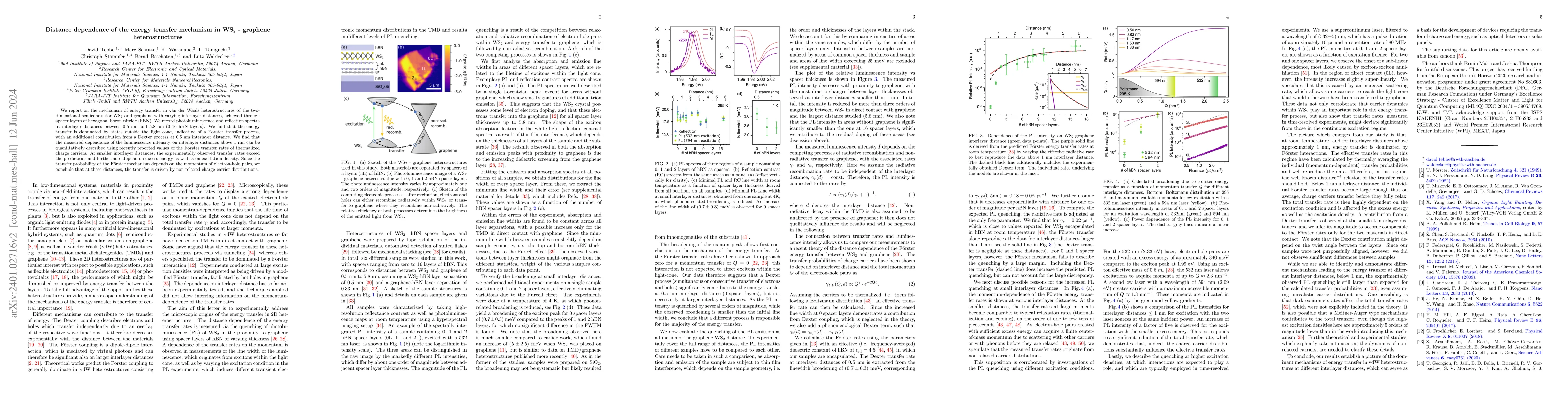
We report on the mechanism of energy transfer in van der Waals heterostructures of the two-dimensional semiconductor WS$_2$ and graphene with varying interlayer distances, achieved through spacer la...

Thumbnail for An open-source robust machine learning platform for real-time detection
  and classification of 2D material flakes
arXiv
An open-source robust machine learning platform for real-time detection and classification of 2D material flakes

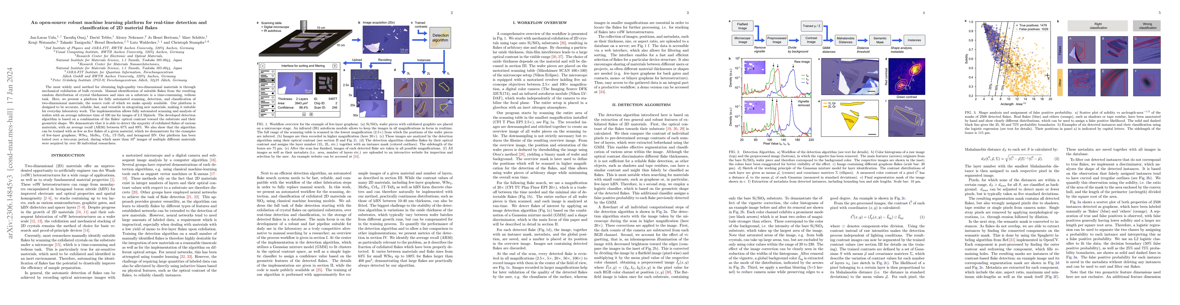
The most widely used method for obtaining high-quality two-dimensional materials is through mechanical exfoliation of bulk crystals. Manual identification of suitable flakes from the resulting rando...

Thumbnail for Spin and Charge Fluctuation Induced Pairing in ABCB Tetralayer Graphene
arXiv
Spin and Charge Fluctuation Induced Pairing in ABCB Tetralayer Graphene

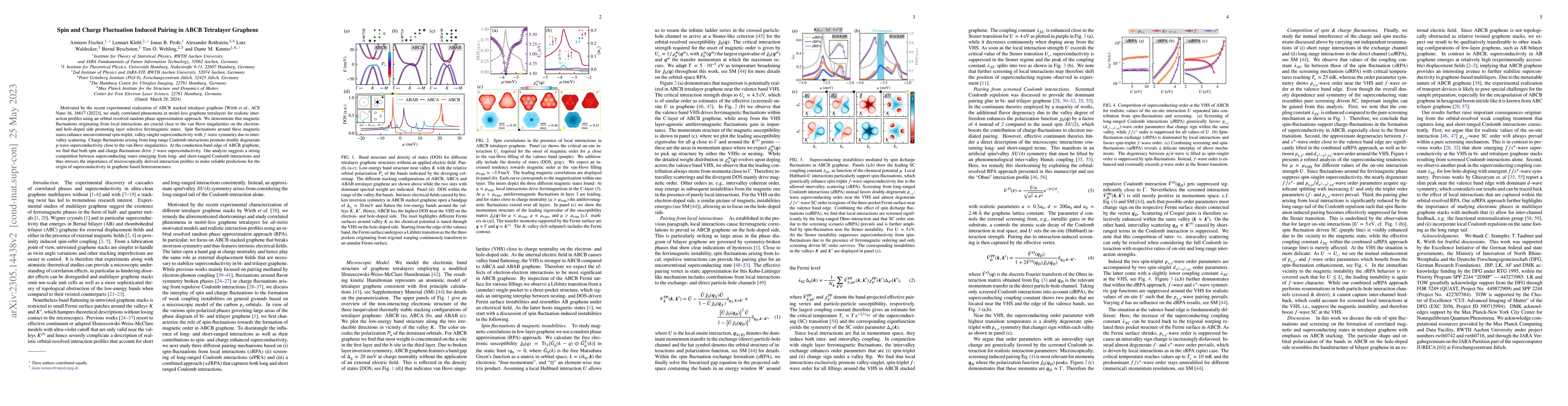
Motivated by the recent experimental realization of ABCB stacked tetralayer graphene [Wirth et al., ACS Nano 16, 16617 (2022)], we study correlated phenomena in moir\'e-less graphene tetralayers for...

Thumbnail for Hyperspectral photoluminescence and reflectance microscopy of 2D
  materials
arXiv
Hyperspectral photoluminescence and reflectance microscopy of 2D materials

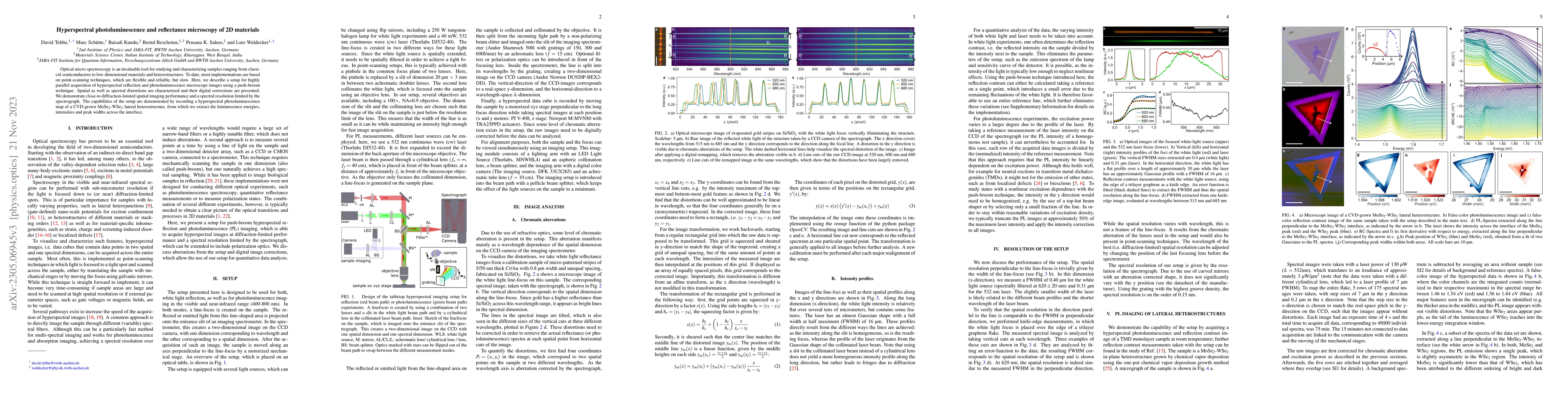
Optical micro-spectroscopy is an invaluable tool for studying and characterizing samples ranging from classical semiconductors to low-dimensional materials and heterostructures. To date, most implem...

Thumbnail for Tailoring the dielectric screening in WS$_2$-graphene heterostructures
arXiv
Tailoring the dielectric screening in WS$_2$-graphene heterostructures

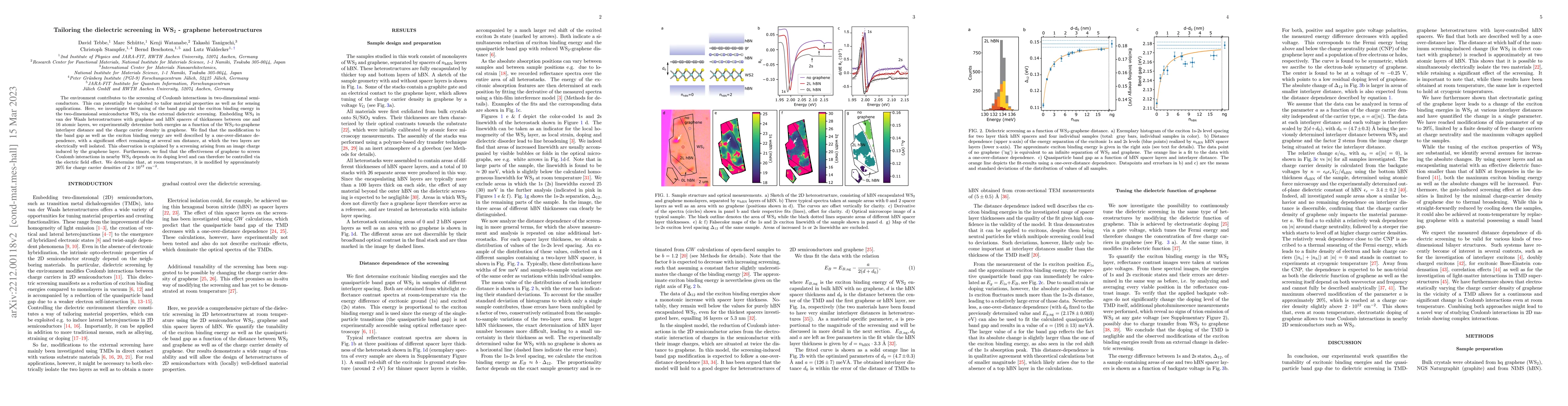
The environment contributes to the screening of Coulomb interactions in two-dimensional semiconductors. This can potentially be exploited to tailor material properties as well as for sensing applica...

Thumbnail for Twist angle dependent interlayer transfer of valley polarization from
  excitons to free charge carriers in WSe$_2$/MoSe$_2$ heterobilayers
arXiv
Twist angle dependent interlayer transfer of valley polarization from excitons to free charge carriers in WSe$_2$/MoSe$_2$ heterobilayers

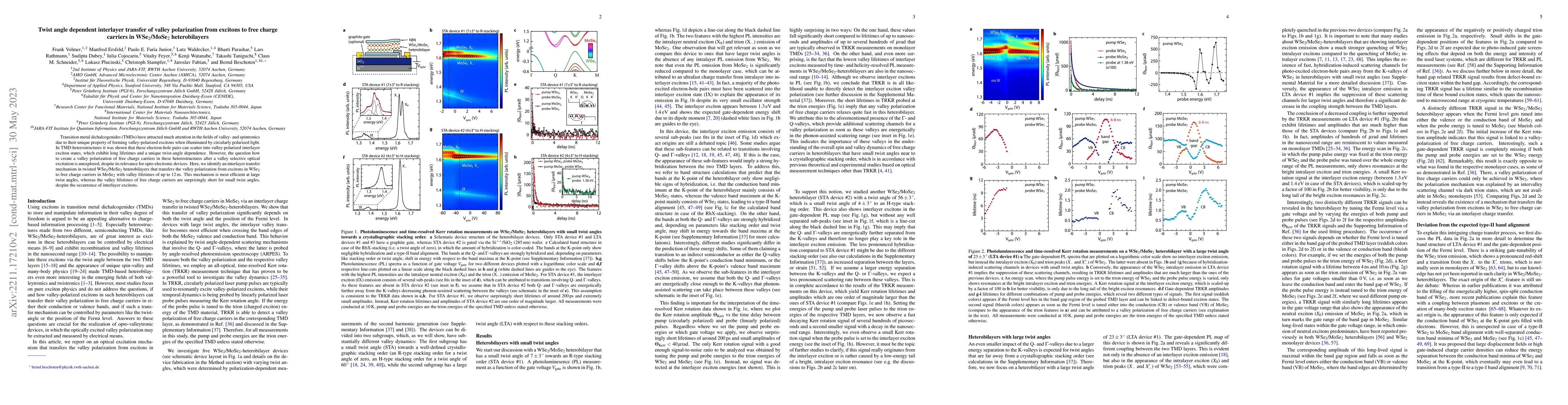
We identify an optical excitation mechanism that transfers a valley polarization from photo-excited electron-hole pairs to free charge carriers in twisted WSe$_2$/MoSe$_2$ heterobilayers. For small ...

Thumbnail for Experimental observation of ABCB stacked tetralayer graphene
arXiv
Experimental observation of ABCB stacked tetralayer graphene

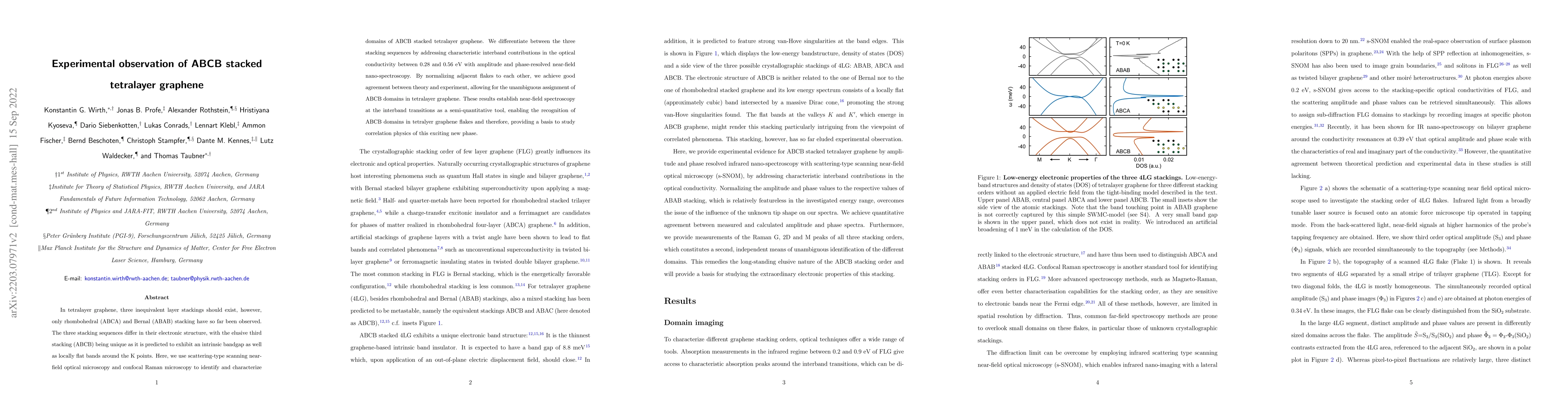
In tetralayer graphene, three inequivalent layer stackings should exist, however, only rhombohedral (ABCA) and Bernal (ABAB) stacking have so far been observed. The three stacking sequences differ i...

Thumbnail for Enhanced nonlinear interaction of polaritons via excitonic Rydberg
  states in monolayer WSe2
arXiv
Enhanced nonlinear interaction of polaritons via excitonic Rydberg states in monolayer WSe2

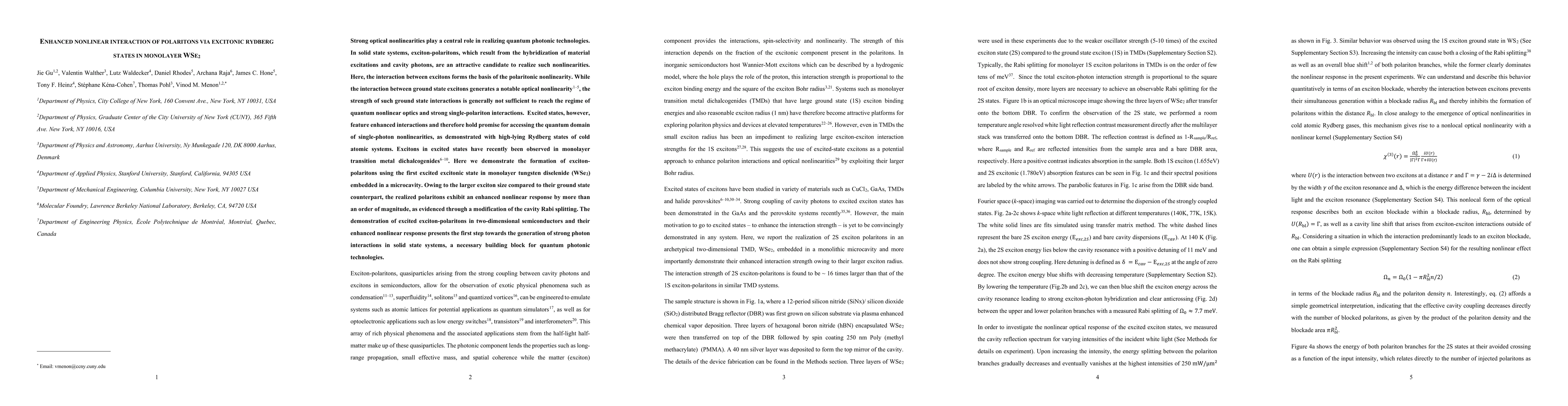
Strong optical nonlinearities play a central role in realizing quantum photonic technologies. In solid state systems, exciton-polaritons, which result from the hybridization of material excitations ...

Thumbnail for Rigid band shifts in two-dimensional semiconductors through
  environmental screening
arXiv
Rigid band shifts in two-dimensional semiconductors through environmental screening

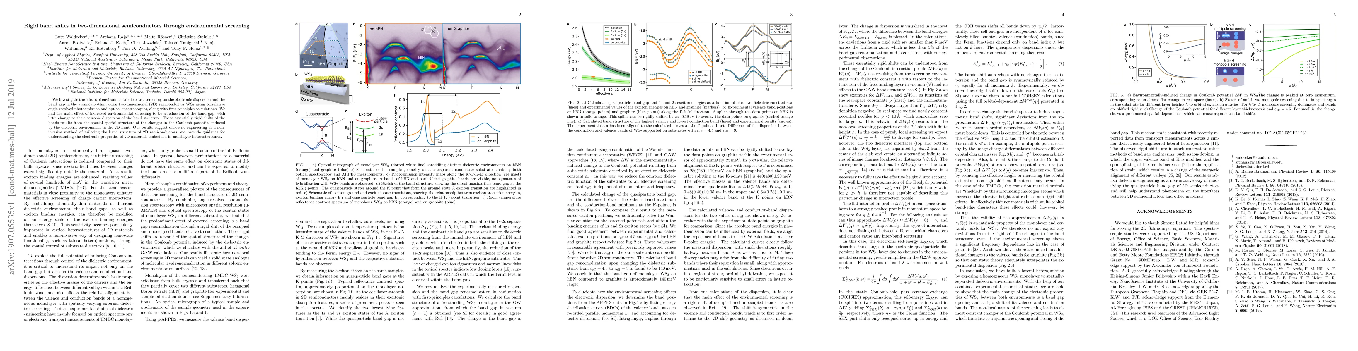
We investigate the effects of environmental dielectric screening on the electronic dispersion and the band gap in the atomically-thin, quasi two-dimensional (2D) semiconductor WS$_2$ using correlati...

Thumbnail for Intrinsic Lifetime of Higher Excitonic States in Tungsten Diselenide
  Monolayers
arXiv
Intrinsic Lifetime of Higher Excitonic States in Tungsten Diselenide Monolayers

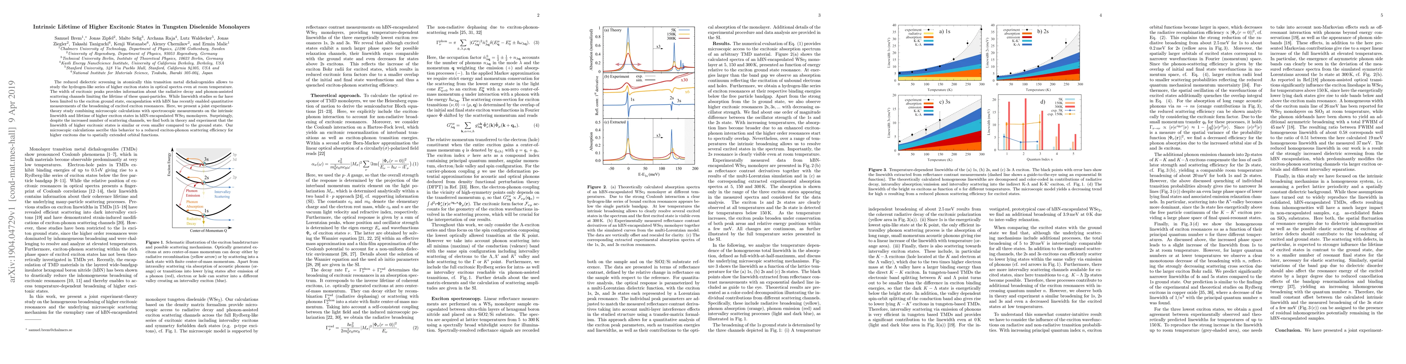
The reduced dielectric screening in atomically thin transition metal dichalcogenides allows to study the hydrogen-like series of higher exciton states in optical spectra even at room temperature. Th...

Thumbnail for Identifying band structure changes of FePS3 across the antiferromagnetic
  phase transition
arXiv
Identifying band structure changes of FePS3 across the antiferromagnetic phase transition

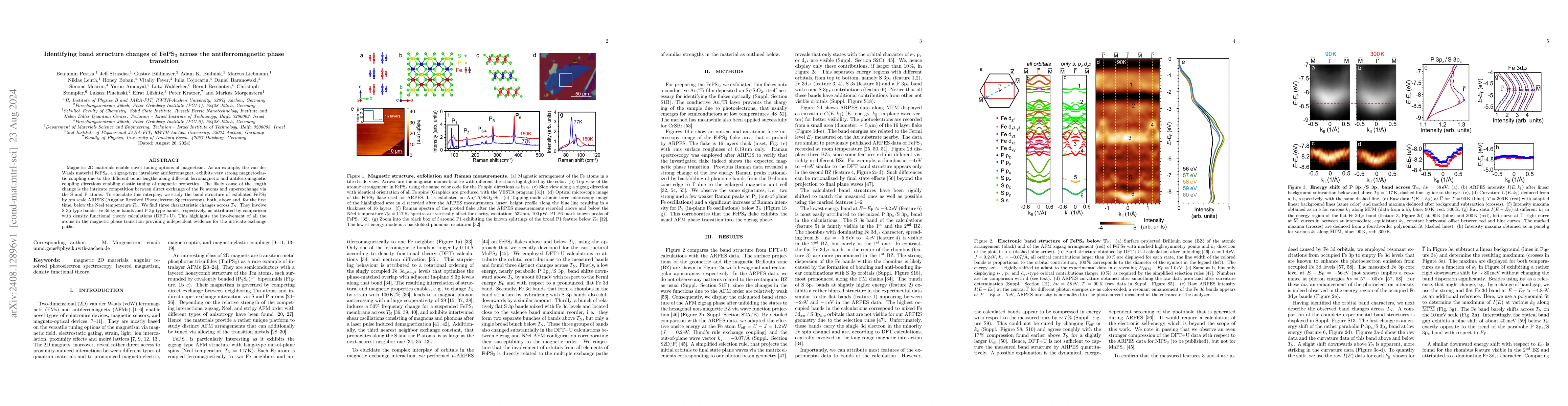
Magnetic 2D materials enable novel tuning options of magnetism. As an example, the van der Waals material FePS3, a zigzag-type intralayer antiferromagnet, exhibits very strong magnetoelastic coupling ...

Thumbnail for Super-resolution imaging of nanoscale inhomogeneities in hBN-covered and
  encapsulated few-layer graphene
arXiv
Super-resolution imaging of nanoscale inhomogeneities in hBN-covered and encapsulated few-layer graphene

Encapsulating few-layer graphene (FLG) in hexagonal boron nitride (hBN) can cause nanoscale inhomogeneities in the FLG, including changes in stacking domains and topographic defects. Due to the diffra...

Thumbnail for MaskTerial: A Foundation Model for Automated 2D Material Flake Detection
arXiv
MaskTerial: A Foundation Model for Automated 2D Material Flake Detection

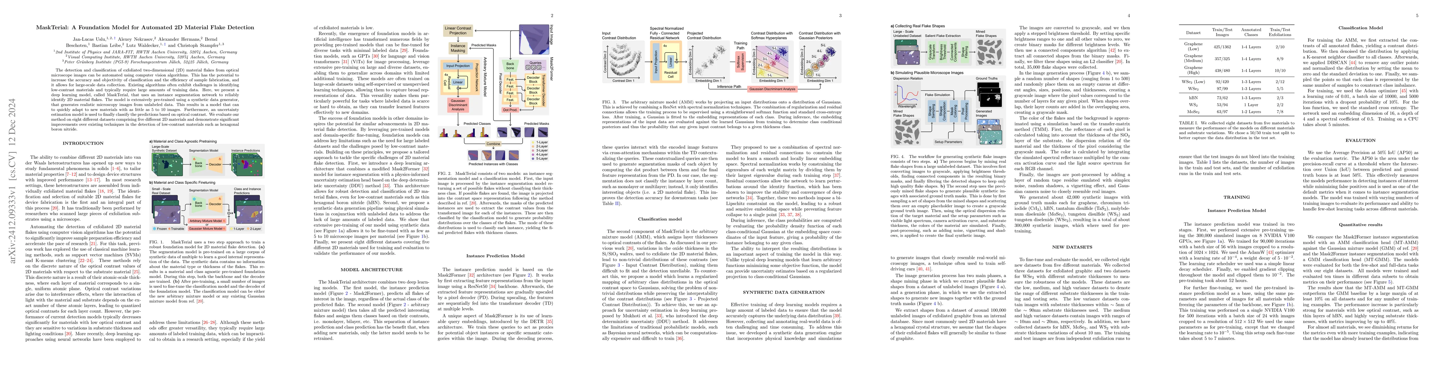
The detection and classification of exfoliated two-dimensional (2D) material flakes from optical microscope images can be automated using computer vision algorithms. This has the potential to increase...

Thumbnail for Electrically Controlled Interfacial Charge Transfer Induced Excitons in
  MoSe2-WSe2 Lateral Heterostructure
arXiv
Electrically Controlled Interfacial Charge Transfer Induced Excitons in MoSe2-WSe2 Lateral Heterostructure

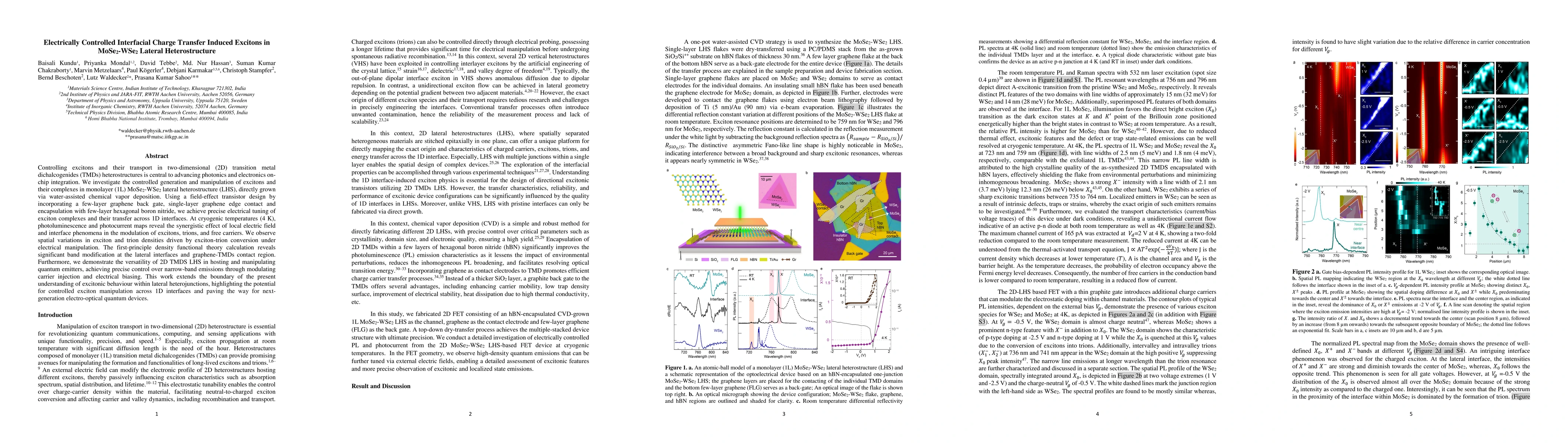
Controlling excitons and their transport in two-dimensional (2D) transition metal dichalcogenides (TMDs) heterostructures is central to advancing photonics and electronics on-chip integration. We inve...

Thumbnail for Probing the band structure of the strongly correlated antiferromagnet
  NiPS3 across its phase transition
arXiv
Probing the band structure of the strongly correlated antiferromagnet NiPS3 across its phase transition

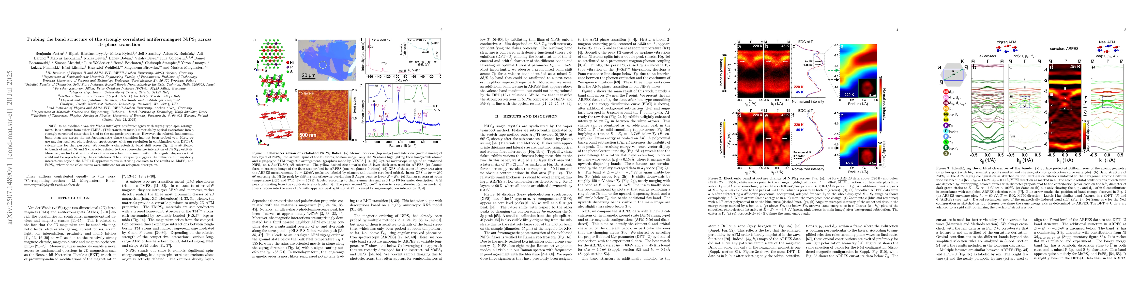
NiPS3 is an exfoliable van-der-Waals intralayer antiferromagnet with zigzag-type spin arrangement. It is distinct from other TMPS3 (TM: transition metal) materials by optical excitations into a strong...

This website uses cookies to ensure you get the best experience. Learn more