Academic Profile
Statistics
Similar Authors
Papers on arXiv
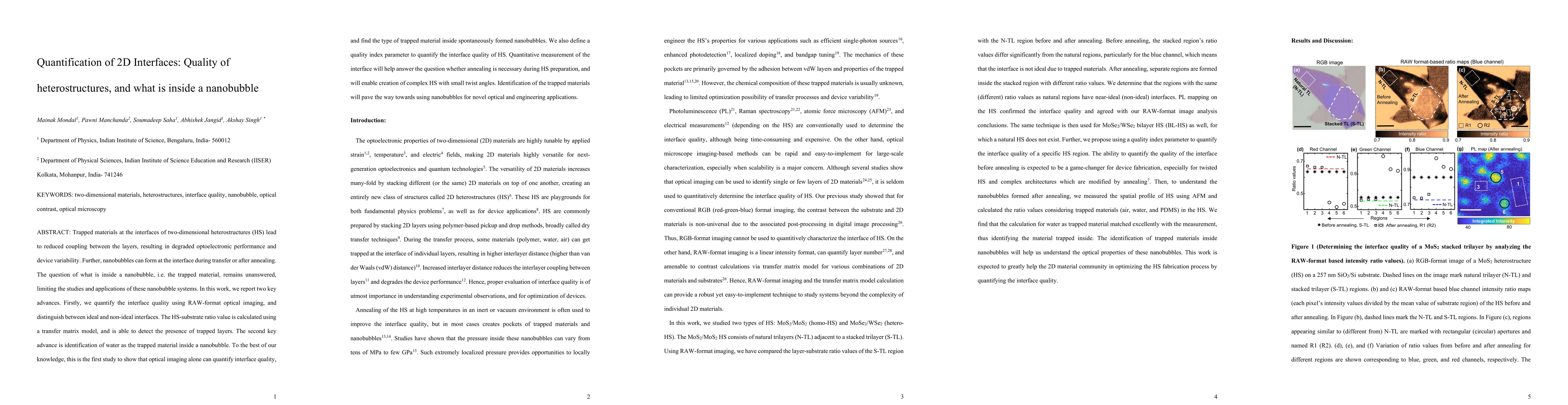
Trapped materials at the interfaces of two-dimensional heterostructures (HS) lead to reduced coupling between the layers, resulting in degraded optoelectronic performance and device variability. Fur...
Control on spatial location and density of defects in 2D materials can be achieved using electron beam irradiation. Conversely, ultralow accelerating voltages (less than or equal to 5kV) are used to...
Optical contrast is the most common preliminary method to identify layer number of two-dimensional (2D) materials, but is seldom used as a confirmatory technique. We explain the reason for variation...
Technological advancement towards the quantum era requires secure communication, quantum computation, and ultra-sensitive sensing capabilities. Layered quantum materials (LQMs) have remarkable optoe...
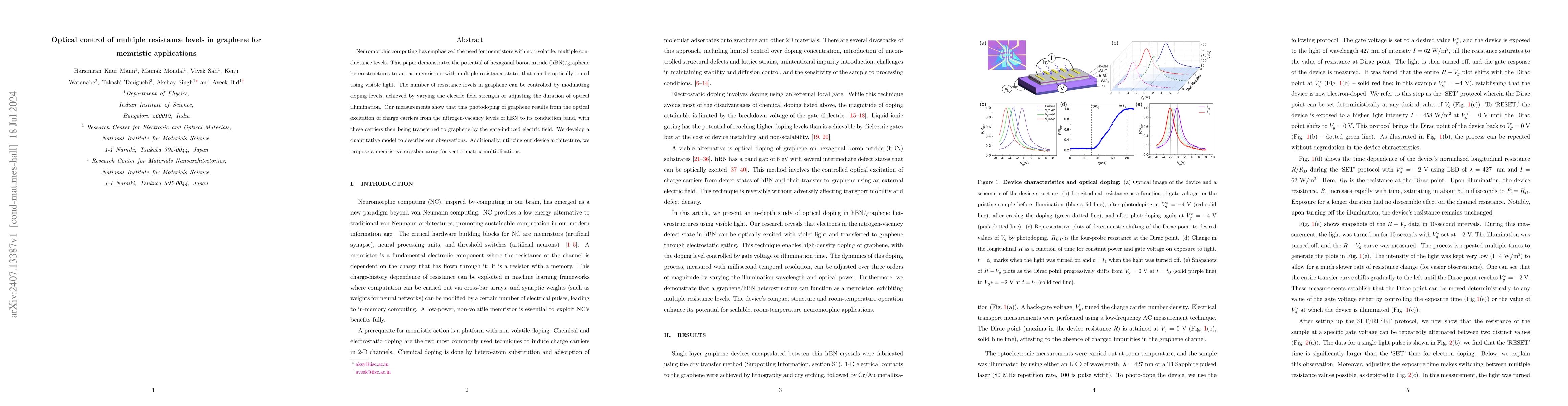
Neuromorphic computing has emphasized the need for memristors with non-volatile, multiple conductance levels. This paper demonstrates the potential of hexagonal boron nitride (hBN)/graphene heterostru...
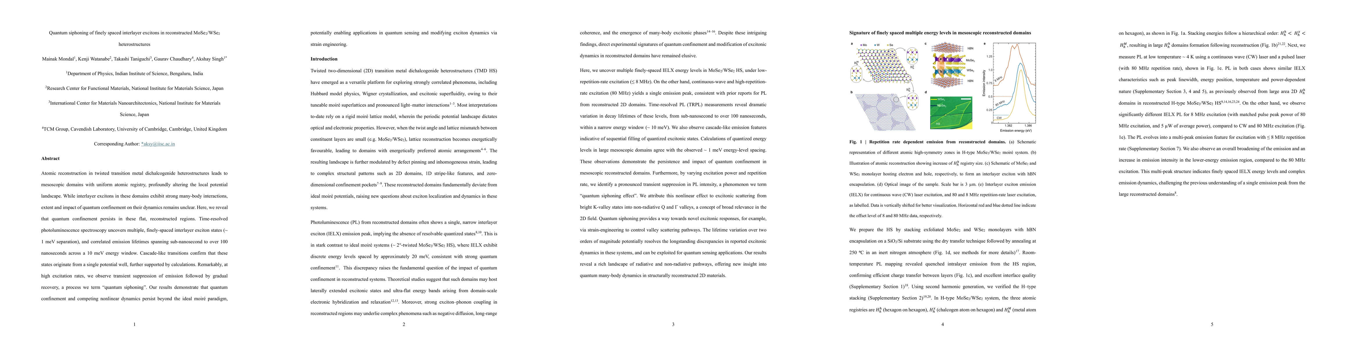
Atomic reconstruction in twisted transition metal dichalcogenide heterostructures leads to mesoscopic domains with uniform atomic registry, profoundly altering the local potential landscape. While int...