ArxivLens
M
Researcher

Manfred Ramsteiner

15 papers on arXiv

15 arXiv Papers
8 Total Publications
Profile

Academic Profile

Name M. Ramsteiner
Total Papers 8
Scholar Profile View on Semantic Scholar
Metrics

Statistics

15 arXiv Papers
8 Total Publications
Publications

Papers on arXiv

Thumbnail for Molecular Beam Epitaxy of GaN Nanowires on Epitaxial Graphene
arXiv
Molecular Beam Epitaxy of GaN Nanowires on Epitaxial Graphene

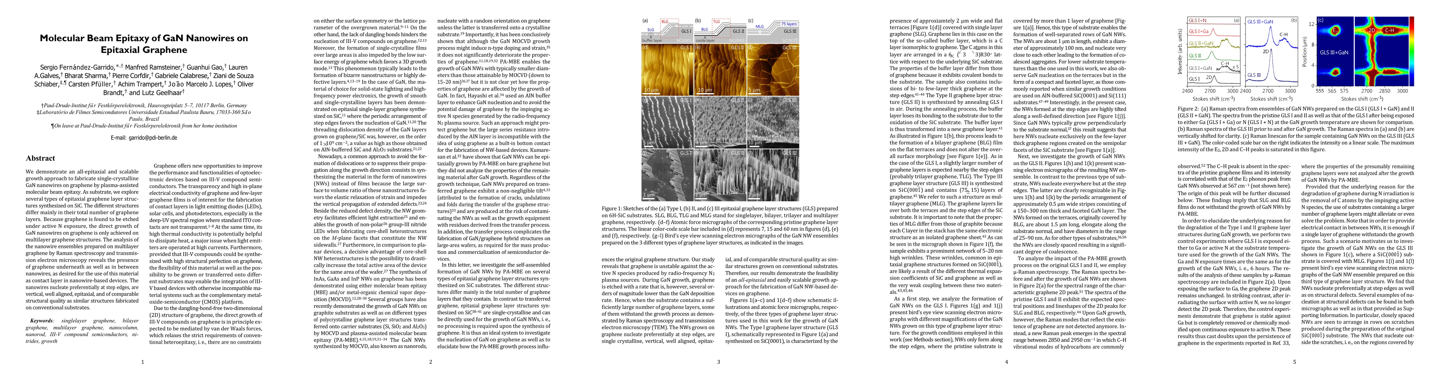
We demonstrate an all-epitaxial and scalable growth approach to fabricate single-crystalline GaN nanowires on graphene by plasma-assisted molecular beam epitaxy. As substrate, we explore several typ...

Thumbnail for In-situ study and modeling of the reaction kinetics during molecular
  beam epitaxy of GeO2 and its etching by Ge
arXiv
In-situ study and modeling of the reaction kinetics during molecular beam epitaxy of GeO2 and its etching by Ge

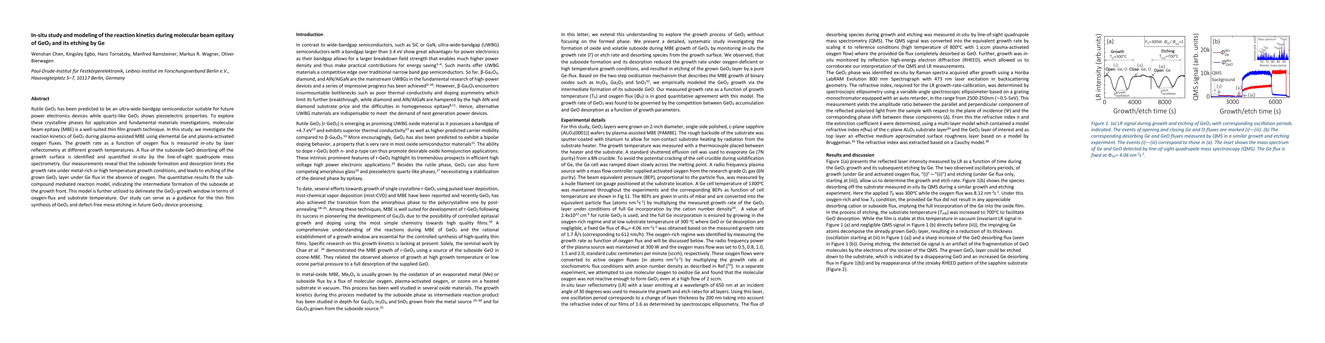
Rutile GeO2 has been predicted to be an ultra-wide bandgap semiconductor suitable for future power electronics devices while quartz-like GeO2 shows piezoelectric properties. To explore these crystal...

Thumbnail for Adsorption-controlled plasma-assisted molecular beam epitaxy of LaInO3
  on DyScO3(110): Growth window, strain relaxation, and domain pattern
arXiv
Adsorption-controlled plasma-assisted molecular beam epitaxy of LaInO3 on DyScO3(110): Growth window, strain relaxation, and domain pattern

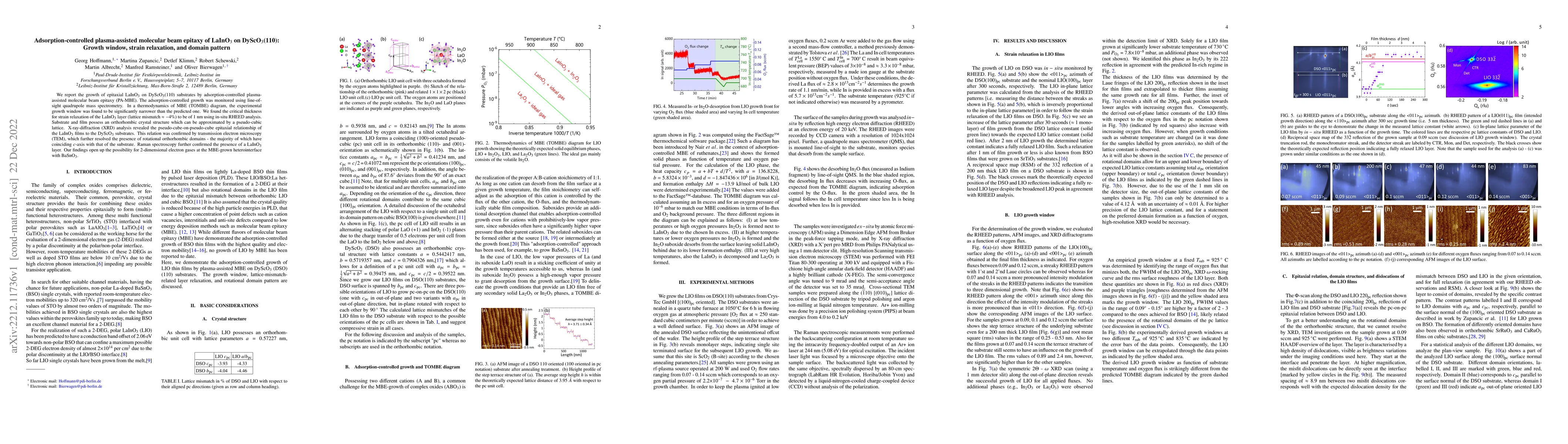
We report the growth of epitaxial LaInO3 on DyScO3(110) substrates by adsorption-controlled plasma-assisted molecular beam epitaxy (PA-MBE). The adsorption-controlled growth was monitored using line...

Thumbnail for Carrier Recombination in Highly Uniform and Phase-Pure GaAs/(Al,Ga)As
  Core/Shell Nanowire Arrays on Si(111): Mott Transition and Internal Quantum
  Efficiency
arXiv
Carrier Recombination in Highly Uniform and Phase-Pure GaAs/(Al,Ga)As Core/Shell Nanowire Arrays on Si(111): Mott Transition and Internal Quantum Efficiency

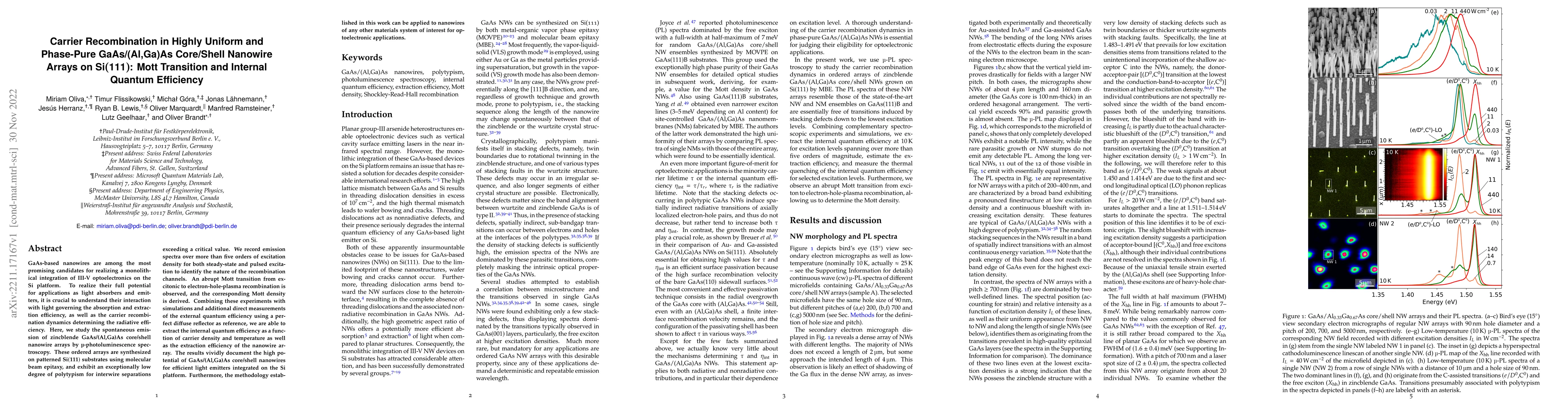
GaAs-based nanowires are among the most promising candidates for realizing a monolithical integration of III-V optoelectronics on the Si platform. To realize their full potential for applications as...

Thumbnail for Density control of GaN nanowires at the wafer scale using self-assembled
  SiN$_x$ patches on sputtered TiN(111)
arXiv
Density control of GaN nanowires at the wafer scale using self-assembled SiN$_x$ patches on sputtered TiN(111)

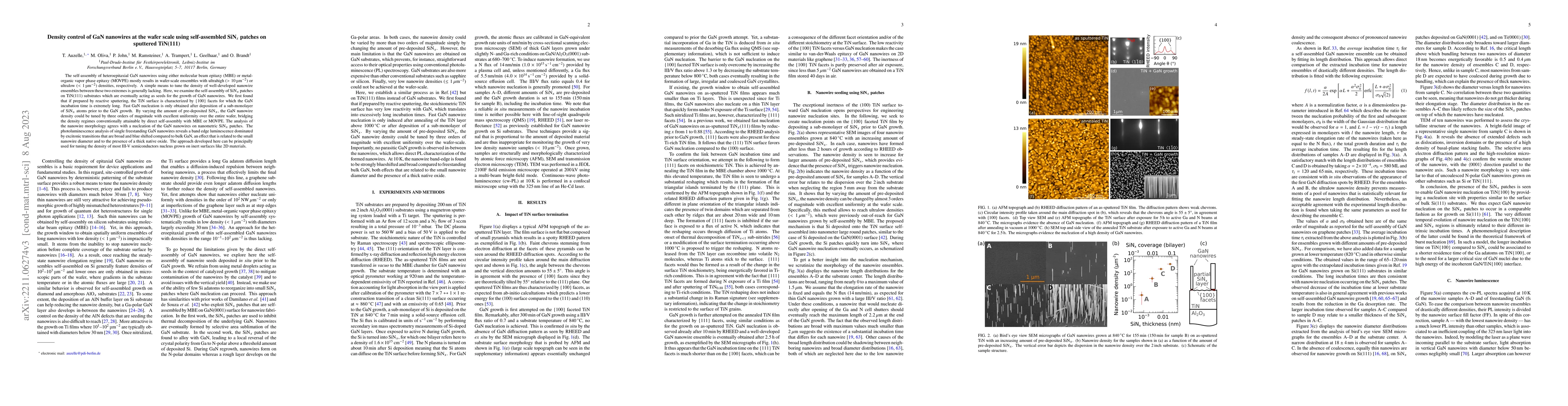
The self-assembly of heteroepitaxial GaN nanowires using either molecular beam epitaxy (MBE) or metal-organic vapor phase epitaxy (MOVPE) mostly results in wafer-scale ensembles with ultrahigh ($>10...

Thumbnail for Molecular beam epitaxy of single-crystalline bixbyite
  (In$_{1-x}$Ga$_x$)$_2$O$_3$ films ($x \leq 0.18$): Structural properties and
  consequences of compositional inhomogeneity
arXiv
Molecular beam epitaxy of single-crystalline bixbyite (In$_{1-x}$Ga$_x$)$_2$O$_3$ films ($x \leq 0.18$): Structural properties and consequences of compositional inhomogeneity

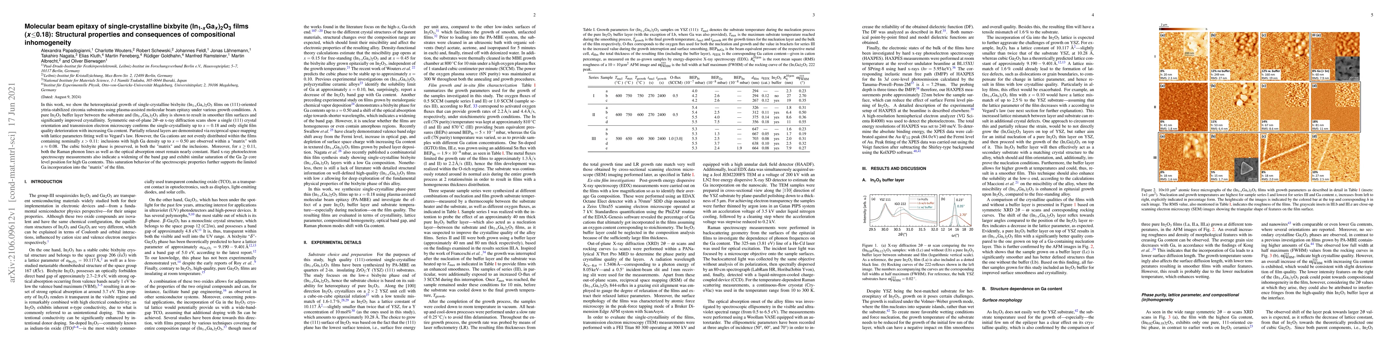
In this work, we show the heteroepitaxial growth of single-crystalline bixbyite (In$_{1-x}$Ga$_x$)$_2$O$_3$ films on (111)-oriented yttria-stabilized zirconia substrates using plasma-assisted molecu...

Thumbnail for Large-area van der Waals epitaxy and magnetic characterization of
  Fe$_3$GeTe$_2$ films on graphene
arXiv
Large-area van der Waals epitaxy and magnetic characterization of Fe$_3$GeTe$_2$ films on graphene

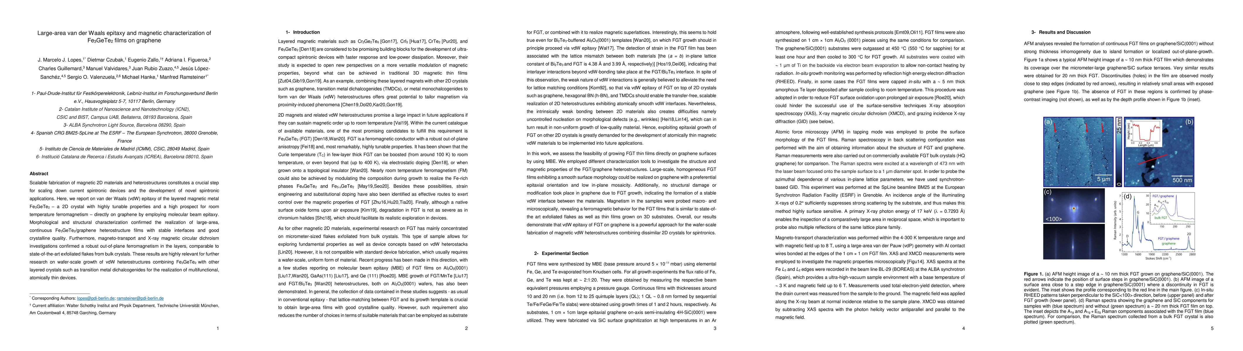
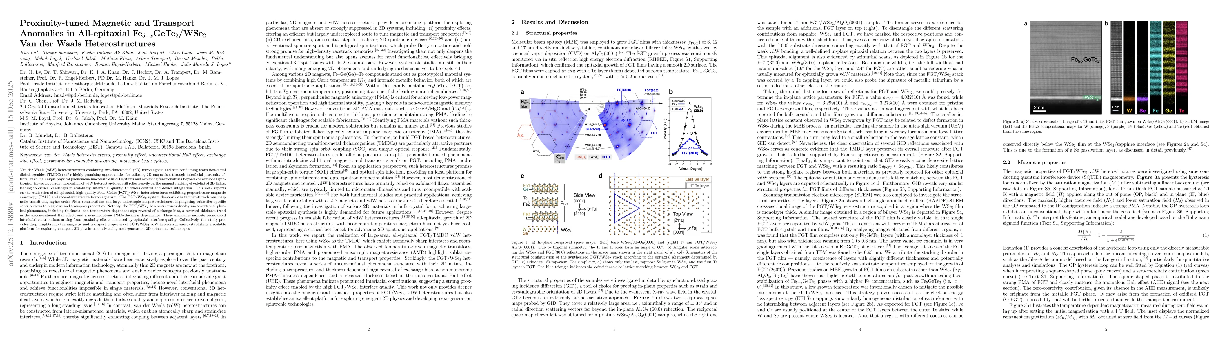
Scalable fabrication of magnetic 2D materials and heterostructures constitutes a crucial step for scaling down current spintronic devices and the development of novel spintronic applications. Here, ...

Thumbnail for SnO/$\beta$-Ga2O3 vertical $pn$ heterojunction diodes
arXiv
SnO/$\beta$-Ga2O3 vertical $pn$ heterojunction diodes

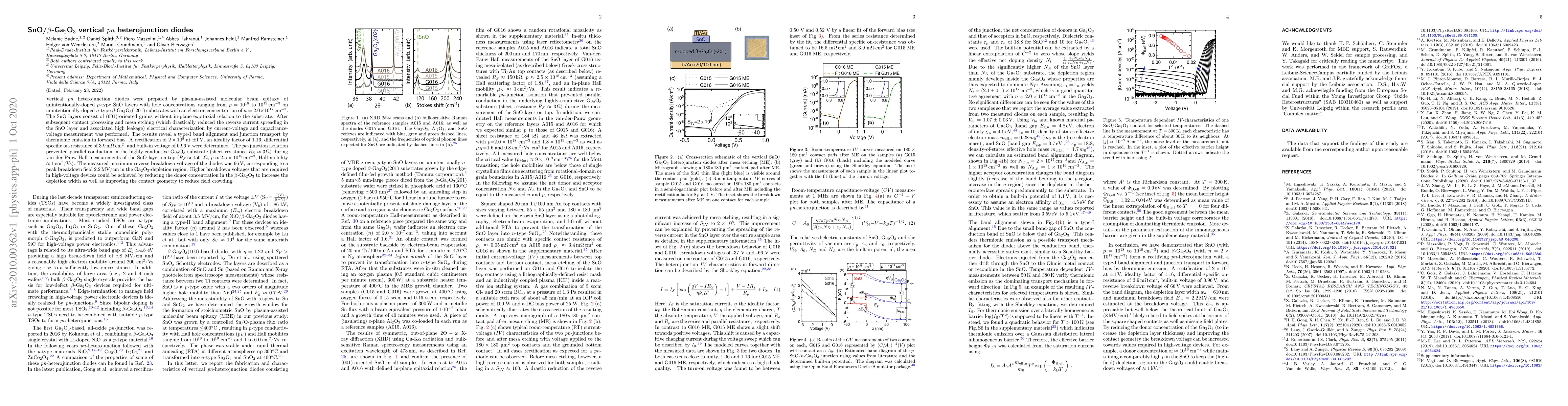
Vertical $pn$ heterojunction diodes were prepared by plasma-assisted molecular beam epitaxy of unintentionally-doped $p$-type SnO layers with hole concentrations ranging from $p=10^{18}$ to $10^{19}...

Thumbnail for Structural, optical, and electrical properties of unintentionally doped
  NiO layers grown on MgO by plasma-assisted molecular beam epitaxy
arXiv
Structural, optical, and electrical properties of unintentionally doped NiO layers grown on MgO by plasma-assisted molecular beam epitaxy

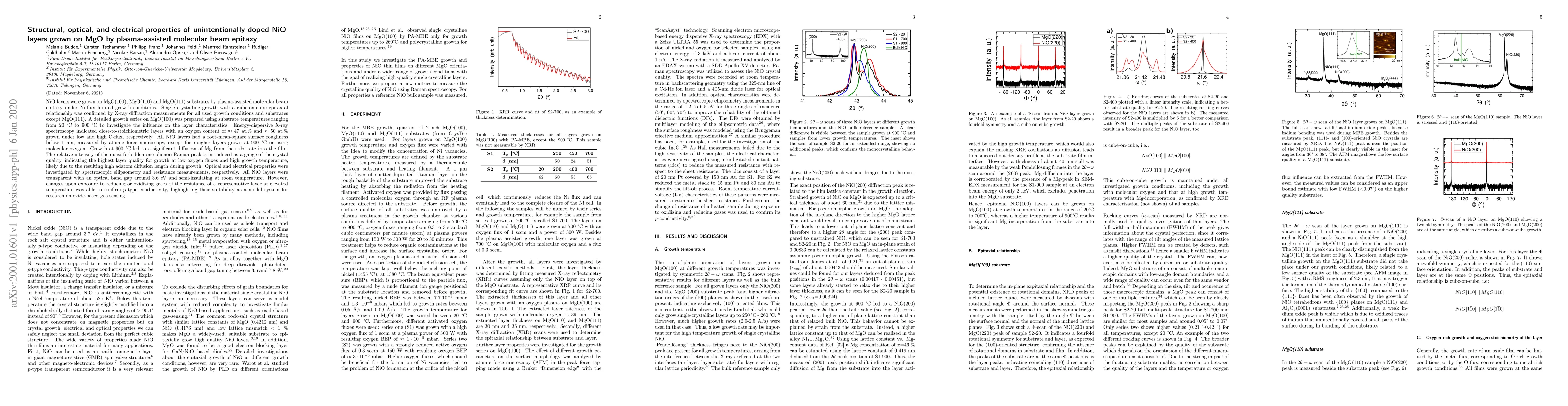
NiO layers were grown on MgO(100), MgO(110), and MgO(111) substrates by plasma-assisted molecular beam epitaxy under Ni-flux limited growth conditions. Single crystalline growth with a cube-on-cube ...

Thumbnail for Plasma-assisted molecular beam epitaxy of NiO on GaN(00.1)
arXiv
Plasma-assisted molecular beam epitaxy of NiO on GaN(00.1)

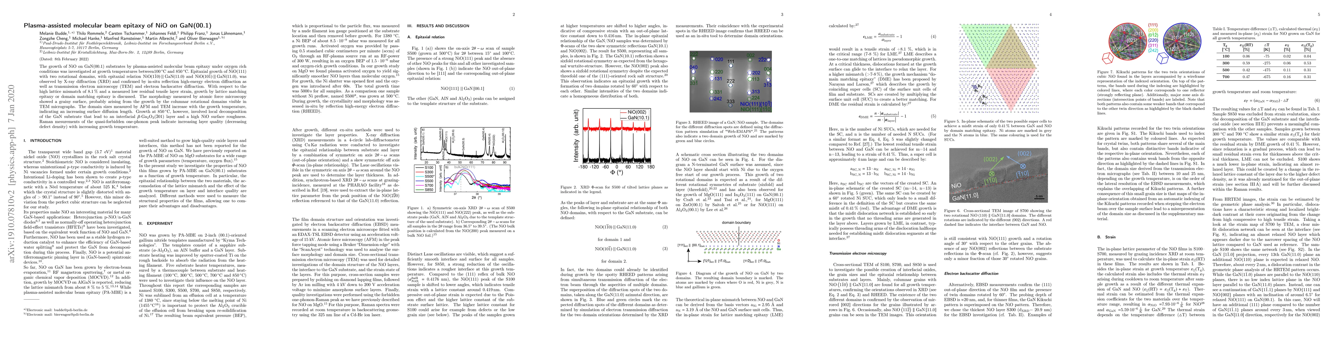
The growth of NiO on GaN(00.1) substrates by plasma-assisted molecular beam epitaxy under oxygen rich conditions was investigated at growth temperatures between 100 $^{\circ}$C and 850 $^{\circ}$C. ...

Thumbnail for Self-assembly of well-separated AlN nanowires directly on sputtered
  metallic TiN films
arXiv
Self-assembly of well-separated AlN nanowires directly on sputtered metallic TiN films

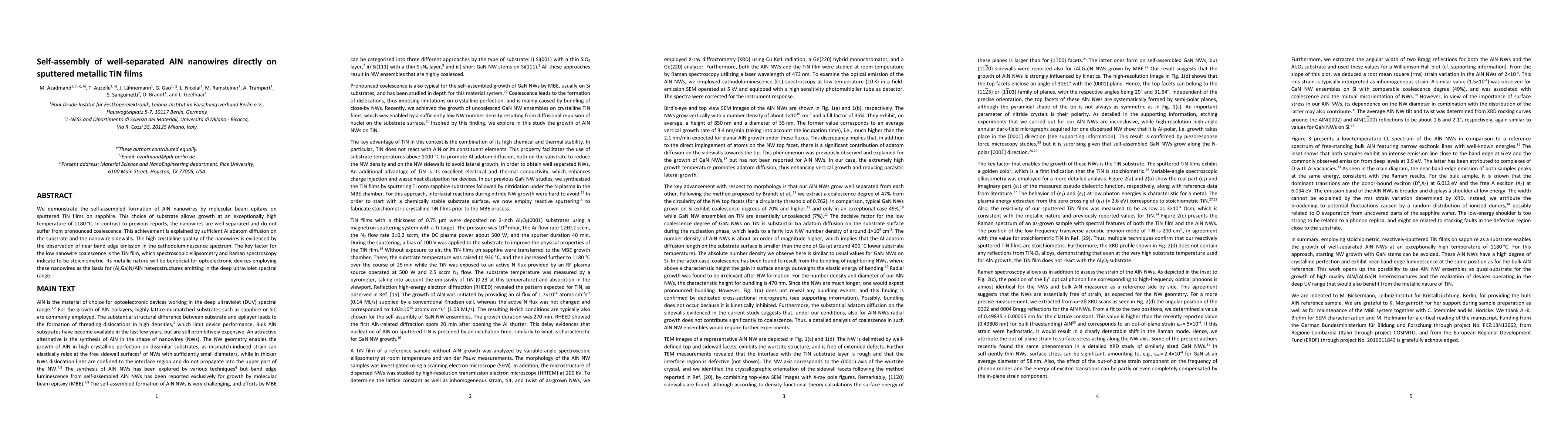
We demonstrate the self-assembled formation of AlN nanowires by molecular beam epitaxy on sputtered TiN films on sapphire. This choice of substrate allows growth at an exceptionally high temperature...
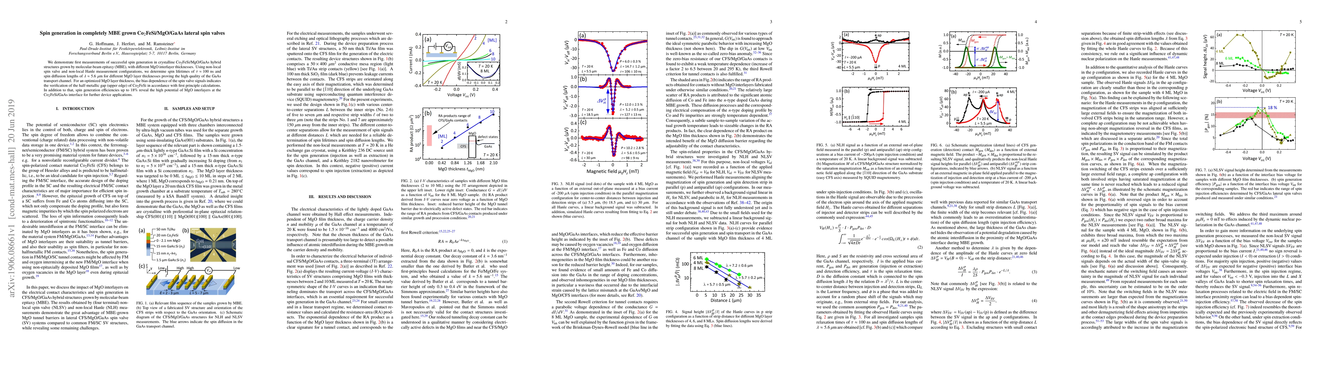
Thumbnail for Signatures of free carriers in Raman spectra of cubic In$_2$O$_3$
arXiv
Signatures of free carriers in Raman spectra of cubic In$_2$O$_3$

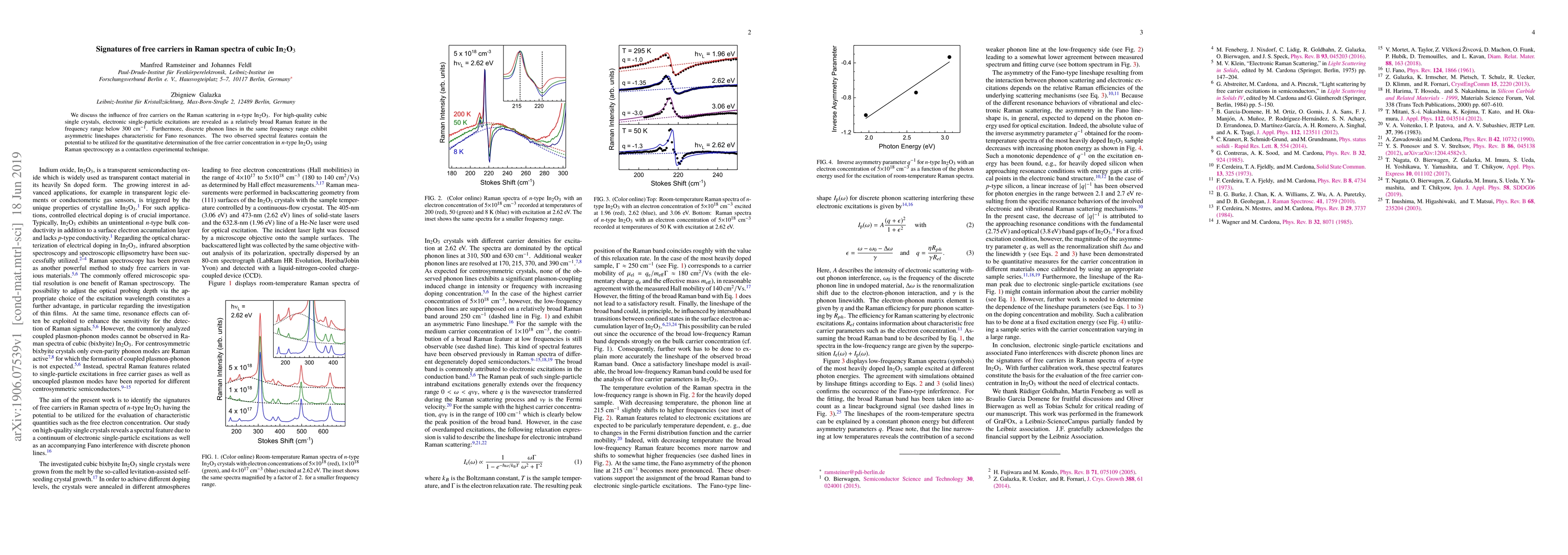
We discuss the influence of free carriers on the Raman scattering in $n$-type In$_2$O$_3$. For high-quality cubic single crystals, electronic single-particle excitations are revealed as a relatively...

Thumbnail for Unravelling the oxygen influence in cubic bixbyite In$_2$O$_3$ on Raman
  active phonon modes by isotope studies
arXiv
Unravelling the oxygen influence in cubic bixbyite In$_2$O$_3$ on Raman active phonon modes by isotope studies

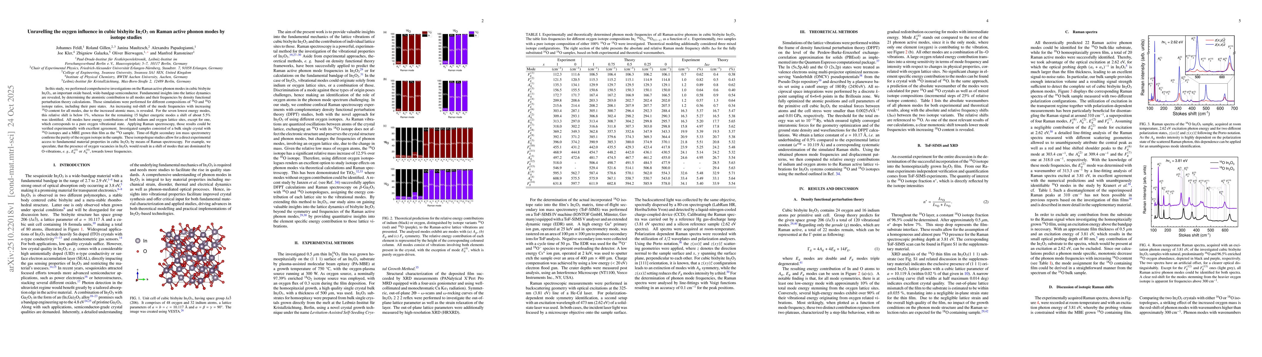
In this study, we performed comprehensive investigations on the Raman active phonon modes in cubic bixbyite In$_2$O$_3$, an important oxide based, wide-bandgap semiconductor. Fundamental insights into...

Thumbnail for Proximity-tuned Magnetic and Transport Anomalies in All-epitaxial Fe5-xGeTe2/WSe2 Van der Waals Heterostructures
arXiv
Proximity-tuned Magnetic and Transport Anomalies in All-epitaxial Fe5-xGeTe2/WSe2 Van der Waals Heterostructures

Van der Waals (vdW) heterostructures combining two-dimensional (2D) ferromagnets and semiconducting transition-metal dichalcogenides (TMDCs) offer highly promising opportunities for tailoring 2D magne...

Thumbnail for Lattice dynamics and complete polarization analysis of Raman-active modes in LaInO$_3$
arXiv
Lattice dynamics and complete polarization analysis of Raman-active modes in LaInO$_3$

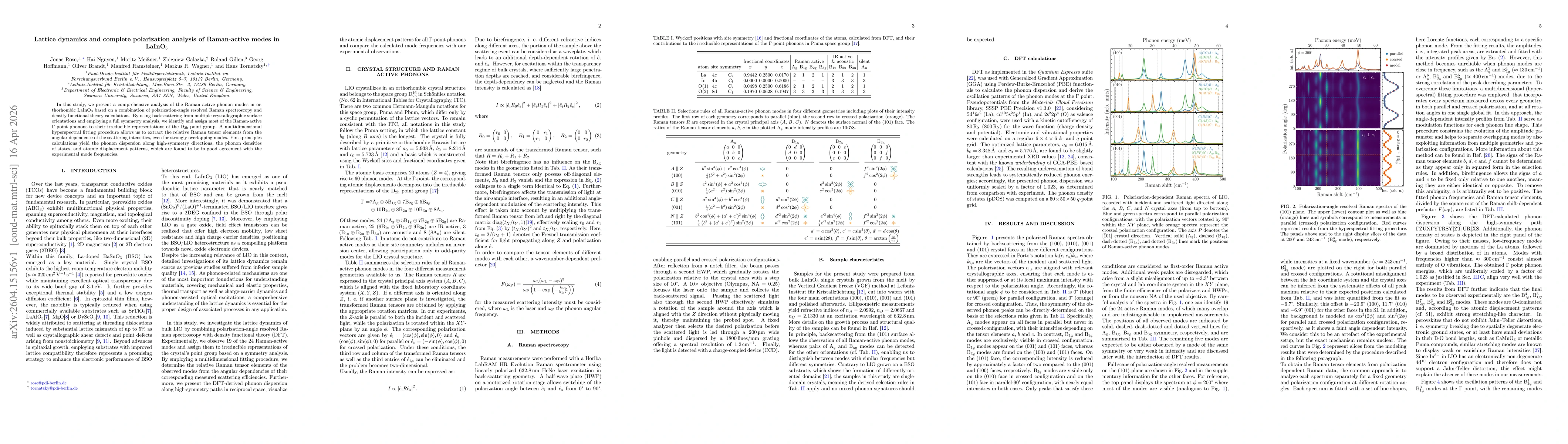
In this study, we present a comprehensive analysis of the Raman active phonon modes in orthorhombic LaInO$_3$ based on a combination of polarization-angle resolved Raman spectroscopy and density funct...

This website uses cookies to ensure you get the best experience. Learn more