Marco Peres

10 papers on arXiv

Academic Profile

Name: M. A. Peres
Total Papers: 25

Statistics

arXiv Papers 10
Total Publications 25

Papers on arXiv

Thumbnail for Microtubes and nanomembranes by ion-beam-induced exfoliation of
  $β$-Ga$_{2}$O$_{3}$

Microtubes and nanomembranes by ion-beam-induced exfoliation of $β$-Ga$_{2}$O$_{3}$

This paper reports an innovative process to fabricate $\beta$-Ga$_{2}$O$_{3}$ microtubes and nanomembranes based on ion implantation in (100)-oriented single-crystals. We show that, under specific flu...

Thumbnail for Effect of Annealing on Al Diffusion and its Impact on the Properties of
  Ga$_2$O$_3$ Thin Films Deposited on c-plane Sapphire by RF Sputtering

Effect of Annealing on Al Diffusion and its Impact on the Properties of Ga$_2$O$_3$ Thin Films Deposited on c-plane Sapphire by RF Sputtering

Gallium oxide is a wide-bandgap semiconductor which has been steadily growing in popularity due to its ultra-wide bandgap, suitability for harsh environments and distinctive opto-electrical properties...

Thumbnail for UV photodetectors and field-effect transistors based on
  $β$-Ga$_2$O$_3$ nanomembranes produced by ion-beam-assisted exfoliation

UV photodetectors and field-effect transistors based on $β$-Ga$_2$O$_3$ nanomembranes produced by ion-beam-assisted exfoliation

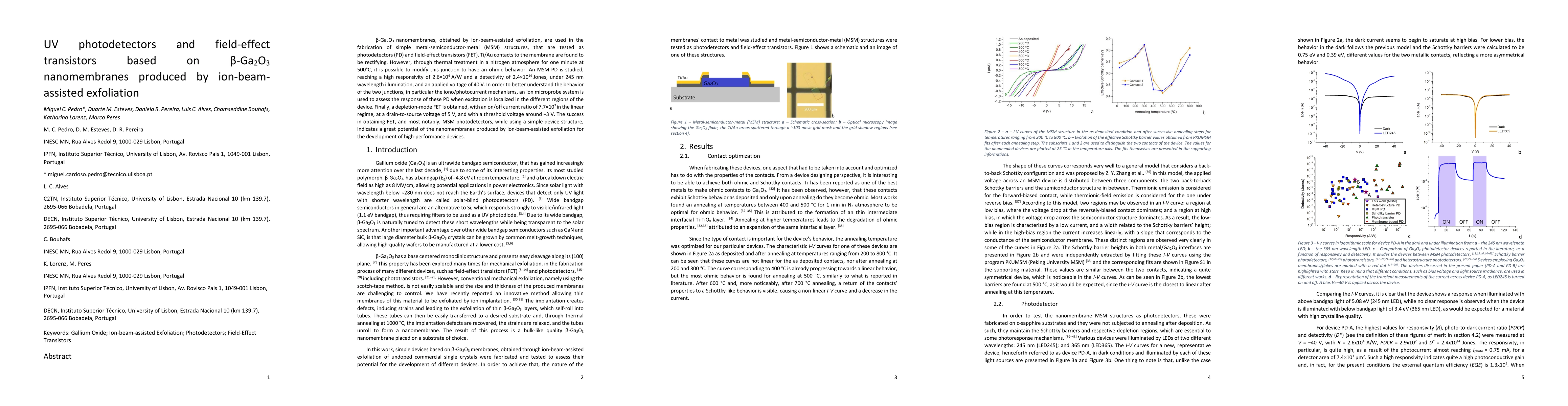
$\beta$-Ga$_{2}$O$_{3}$ nanomembranes, obtained by ion-beam-assisted exfoliation, are used in the fabrication of simple metal-semiconductor-metal (MSM) structures, that are tested as photodetectors (P...

Thumbnail for Prediction of synthesis parameters for N, Si, Ge and Sn diamond vacancy
  centers using machine learning

Prediction of synthesis parameters for N, Si, Ge and Sn diamond vacancy centers using machine learning

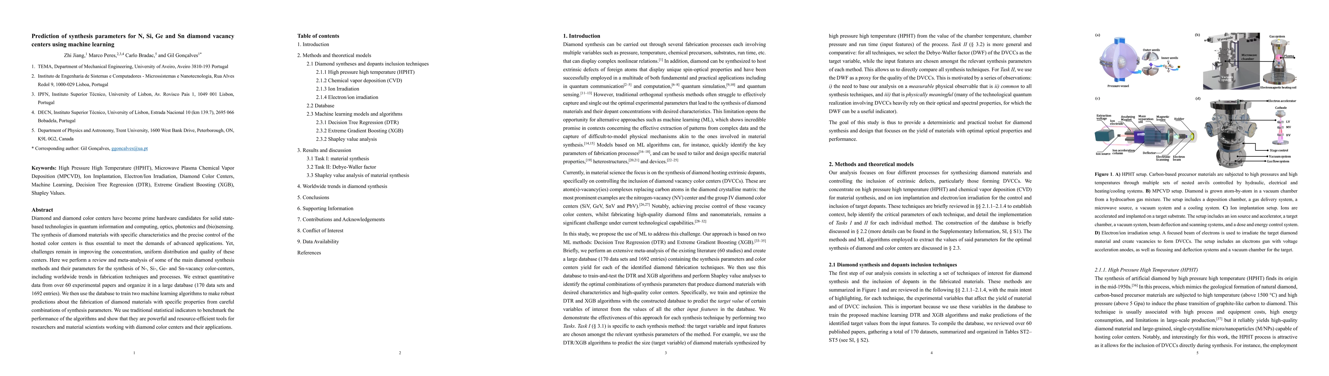
Diamond and diamond color centers have become prime hardware candidates for solid state-based technologies in quantum information and computing, optics, photonics and (bio)sensing. The synthesis of di...

Thumbnail for Silicon Driven Facet Regulation Enables Tunable Micro-Diamond Architectures in Liquid Ga In

Silicon Driven Facet Regulation Enables Tunable Micro-Diamond Architectures in Liquid Ga In

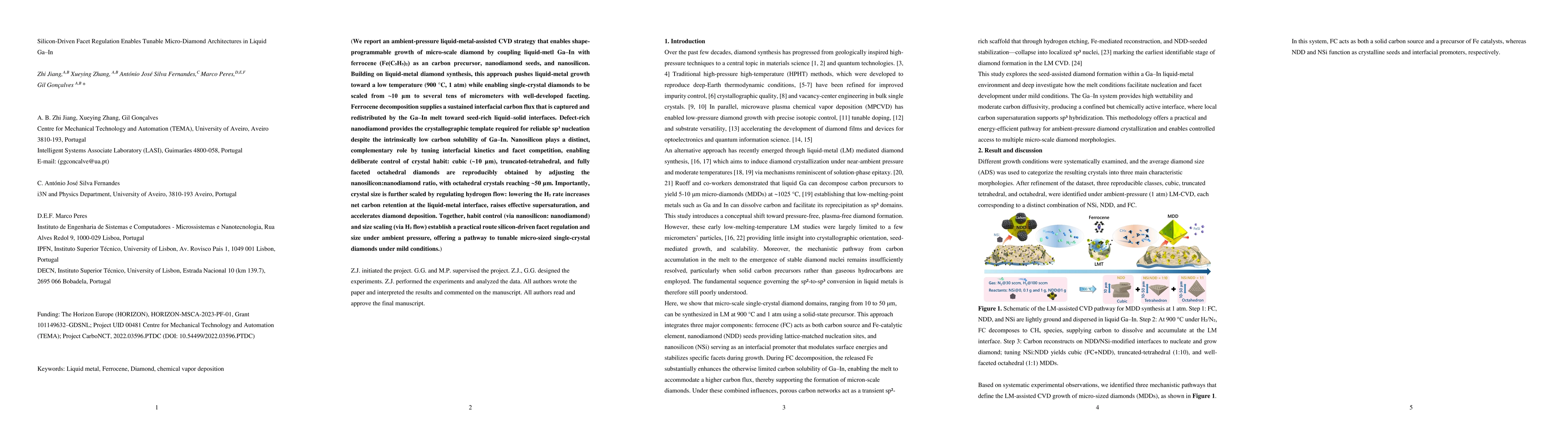
We report an ambient pressure liquid metal assisted CVD strategy that enables shape programmable growth of micro scale diamond by coupling liquid metl Ga In with ferrocene (Fe(C5H5)2) as an carbon pre...

Thumbnail for Study on the Effect of Annealing on Ga$_2$O$_3$ Thin Films Deposited on Silicon by RF Sputtering

Study on the Effect of Annealing on Ga$_2$O$_3$ Thin Films Deposited on Silicon by RF Sputtering

Gallium oxide is an ultra-wide bandgap semiconductor with excellent opto-electronic properties, making it a highly promising material for a wide range of applications and devices. In this article, we ...

Thumbnail for Understanding the anisotropic response of $β$-Ga$_2$O$_3$ to ion implantation

Understanding the anisotropic response of $β$-Ga$_2$O$_3$ to ion implantation

While $β$-Ga$_2$O$_3$ is considered a promising wide bandgap semiconductor, the impact of ion-induced defect formation and anisotropic elasticity remains poorly understood. Here, we combine a simulati...

Thumbnail for Au and Ag nanoparticles produced by ion implantation in single-crystalline $β$-Ga$_2$O$_3$

Au and Ag nanoparticles produced by ion implantation in single-crystalline $β$-Ga$_2$O$_3$

This work reports the successful formation of Ag and Au nanoparticles in $β$-Ga$_2$O$_3$ single-crystals by ion implantation and annealing at 550 °C. X-ray diffraction measurements revealed that nanop...

Thumbnail for Anisotropic implantation damage build-up and crystal recovery in $β$-Ga$_2$O$_3$

Anisotropic implantation damage build-up and crystal recovery in $β$-Ga$_2$O$_3$

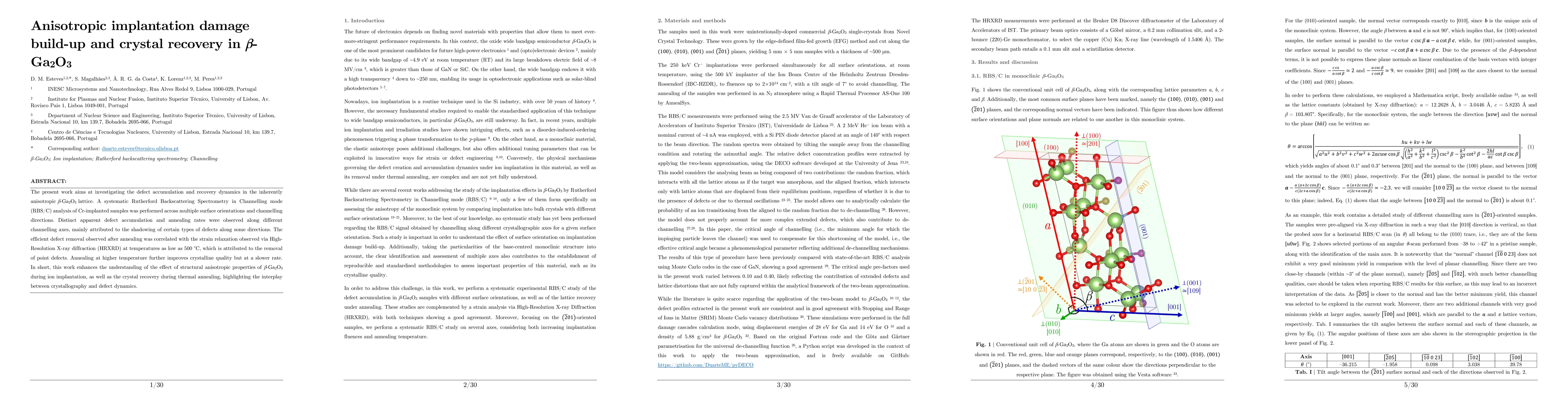
The present work aims at investigating the defect accumulation and recovery dynamics in the inherently anisotropic $β$-Ga$_2$O$_3$ lattice. A systematic Rutherford Backscattering Spectrometry in Chann...

Thumbnail for Formation of Ag and Au Plasmonic Nanoparticles by Ion Implantation in Ga$_2$O$_3$ thin films

Formation of Ag and Au Plasmonic Nanoparticles by Ion Implantation in Ga$_2$O$_3$ thin films

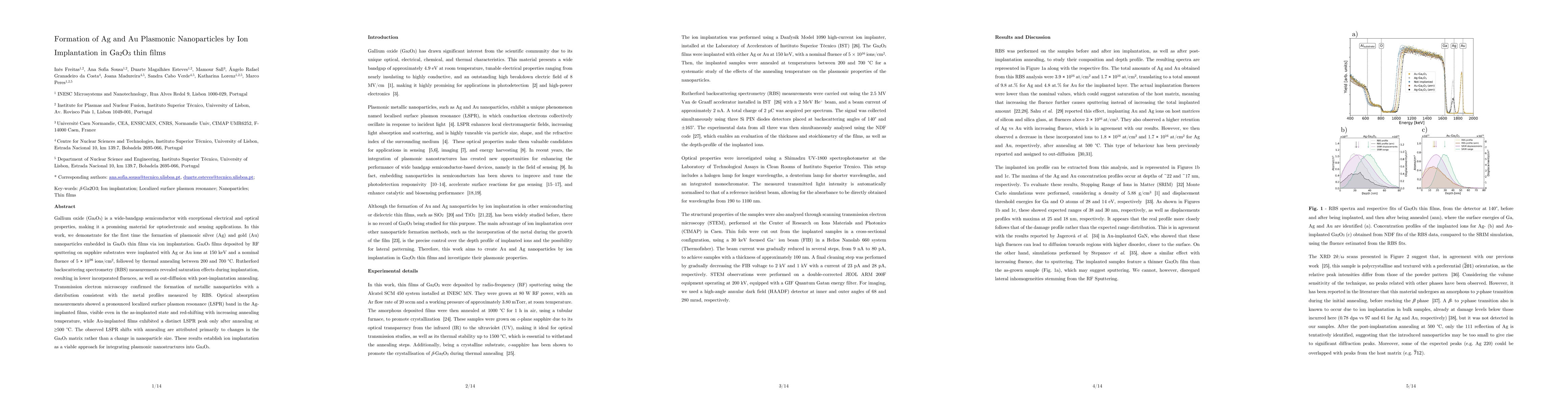
Gallium oxide (Ga$_2$O$_3$) is a wide-bandgap semiconductor with exceptional electrical and optical properties, making it a promising material for optoelectronic and sensing applications. In this work...

This website uses cookies to ensure you get the best experience. Learn more