Academic Profile
Statistics
Similar Authors
Papers on arXiv
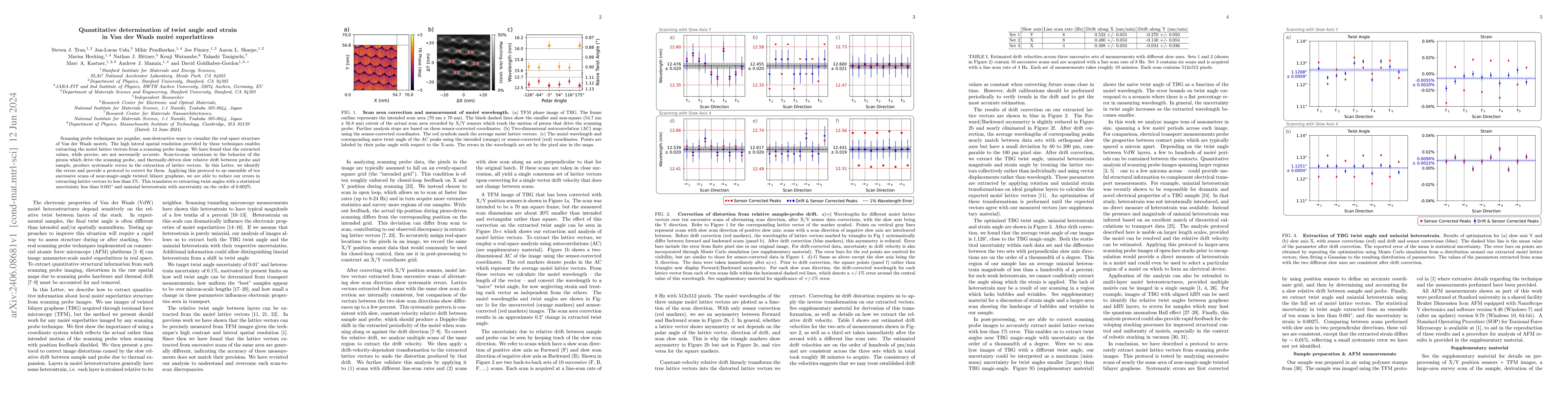
Scanning probe techniques are popular, non-destructive ways to visualize the real space structure of Van der Waals moir\'es. The high lateral spatial resolution provided by these techniques enables ...
The electronic properties of moir\'e heterostructures depend sensitively on the relative orientation between layers of the stack. For example, near-magic-angle twisted bilayer graphene (TBG) commonl...
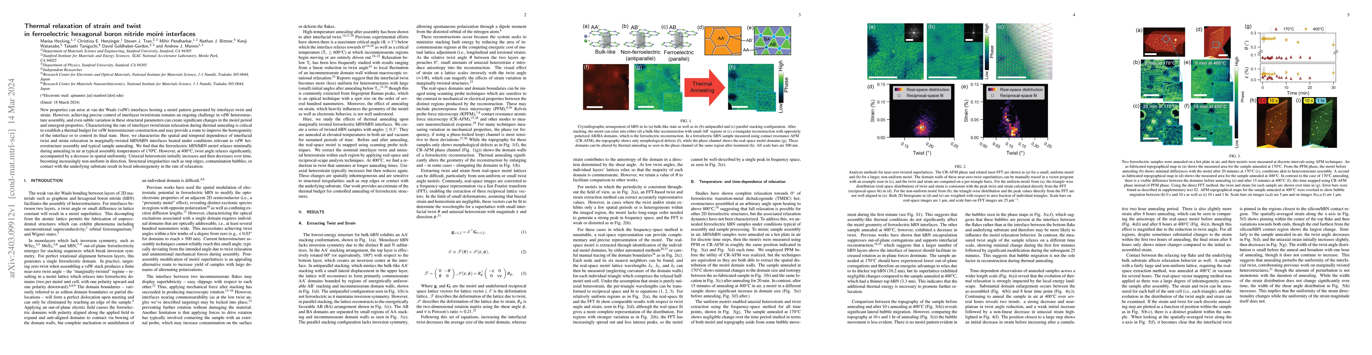
New properties can arise at van der Waals (vdW) interfaces hosting a moir\'e pattern generated by interlayer twist and strain. However, achieving precise control of interlayer twist/strain remains a...
Two-dimensional (2D) semiconducting transition-metal dichalcogenides (TMDCs) are an exciting platform for new excitonic physics and next-generation electronics, creating a strong demand to understan...
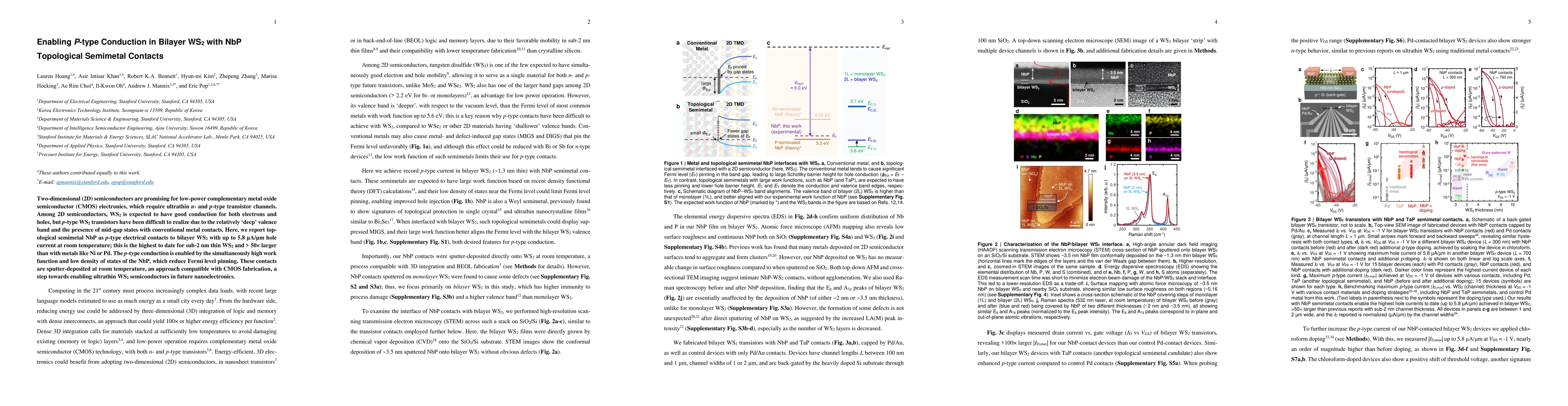
Two-dimensional (2D) semiconductors are promising for low-power complementary metal oxide semiconductor (CMOS) electronics, which require ultrathin n- and p-type transistor channels. Among 2D semicond...
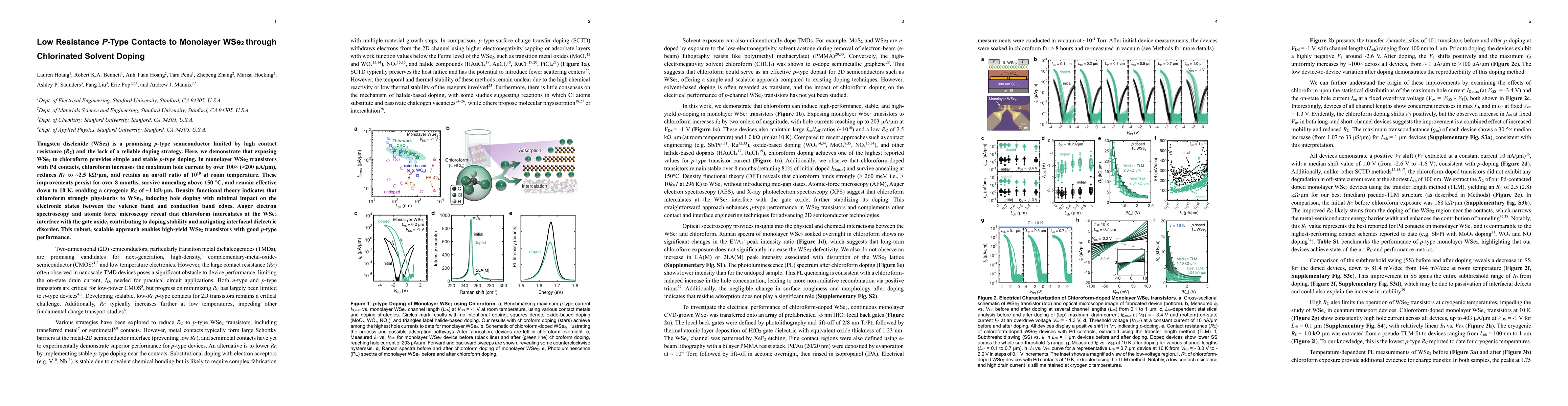
Tungsten diselenide (WSe$_2$) is a promising p-type semiconductor limited by high contact resistance ($R_\textrm{C}$) and the lack of a reliable doping strategy. Here, we demonstrate that exposing WSe...
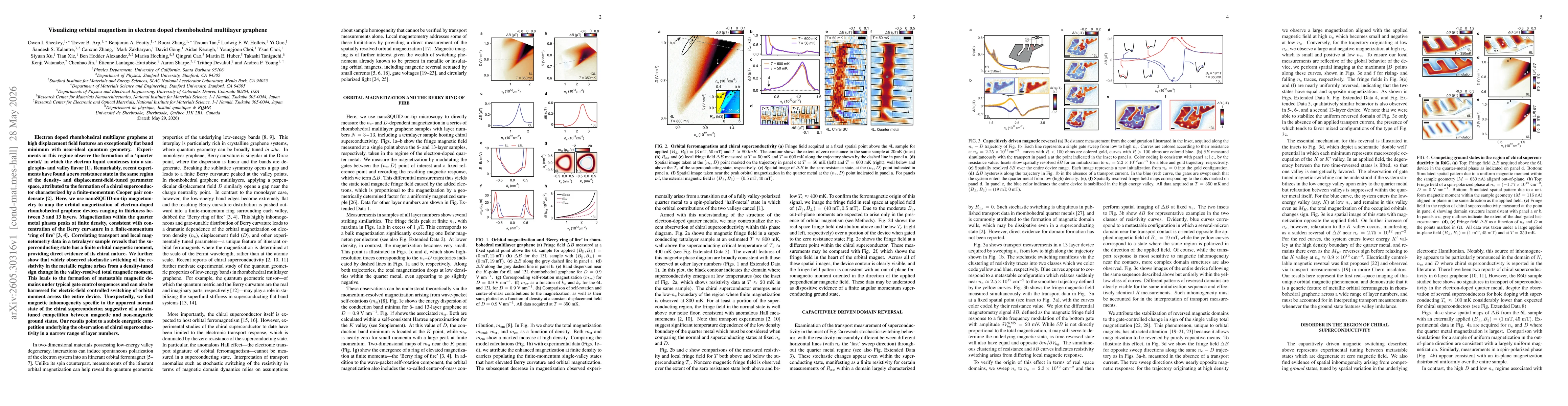
Electron doped rhombohedral multilayer graphene at high displacement field features an exceptionally flat band minimum with near-ideal quantum geometry. Experiments in this regime observe the formatio...
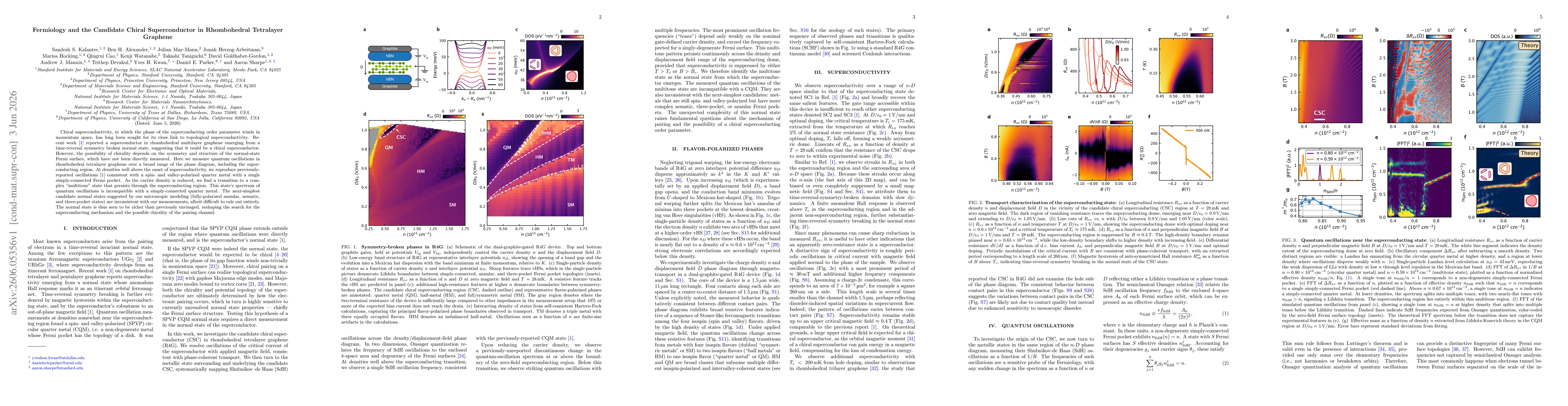
Chiral superconductivity, in which the phase of the superconducting order parameter winds in momentum space, has long been sought for its close link to topological superconductivity. Recent work repor...