Academic Profile
Statistics
Similar Authors
Papers on arXiv
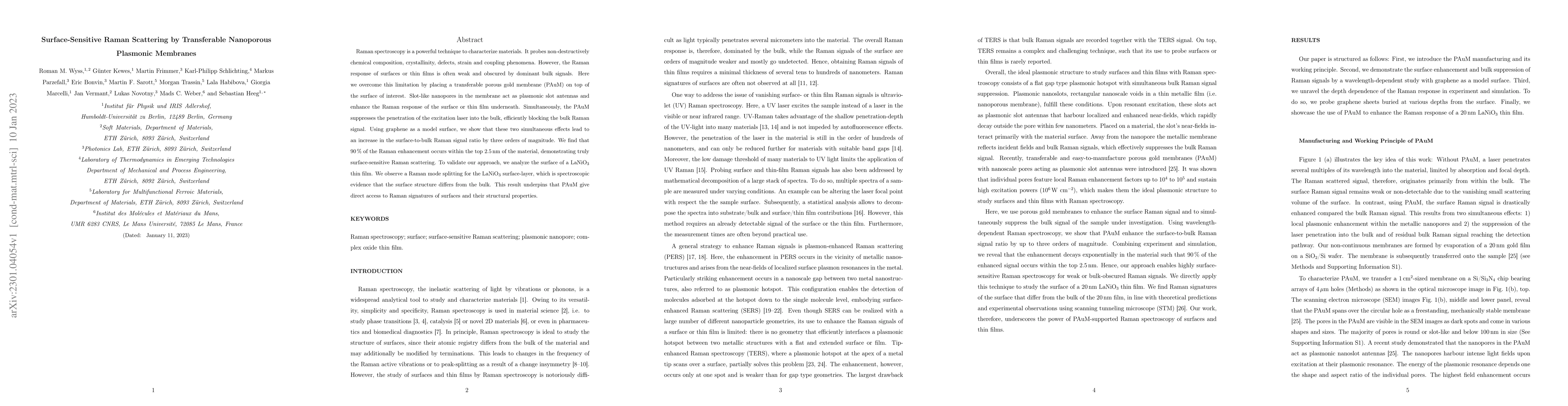
Raman spectroscopy is a powerful technique to characterize materials. It probes non-destructively chemical composition, crystallinity, defects, strain and coupling phenomena. However, the Raman resp...
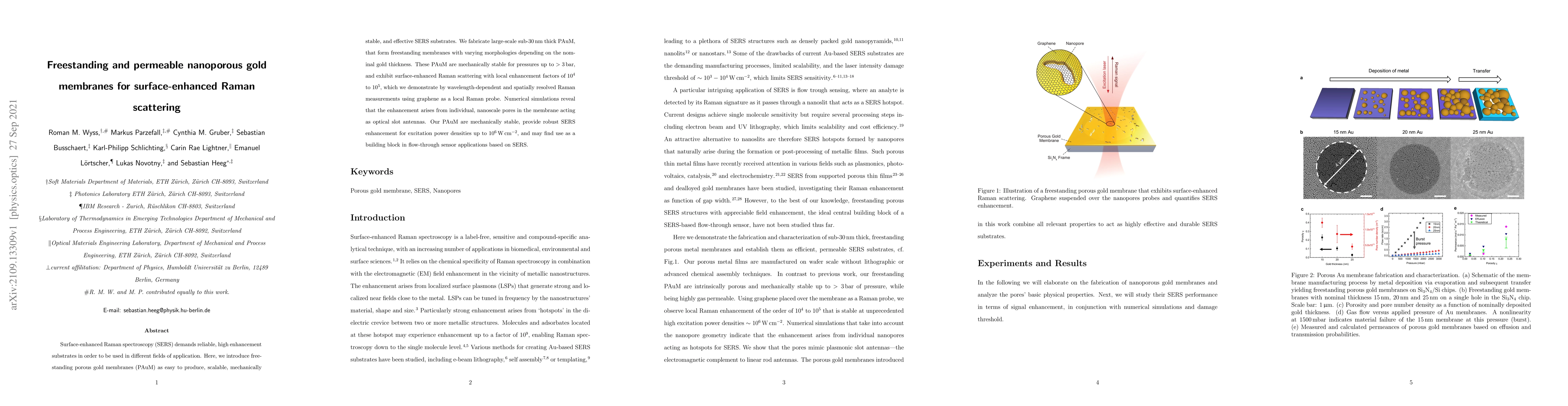
Surface-enhanced Raman spectroscopy (SERS) demands reliable, high enhancement substrates in order to be used in different fields of application. Here, we introduce freestanding porous gold membranes...
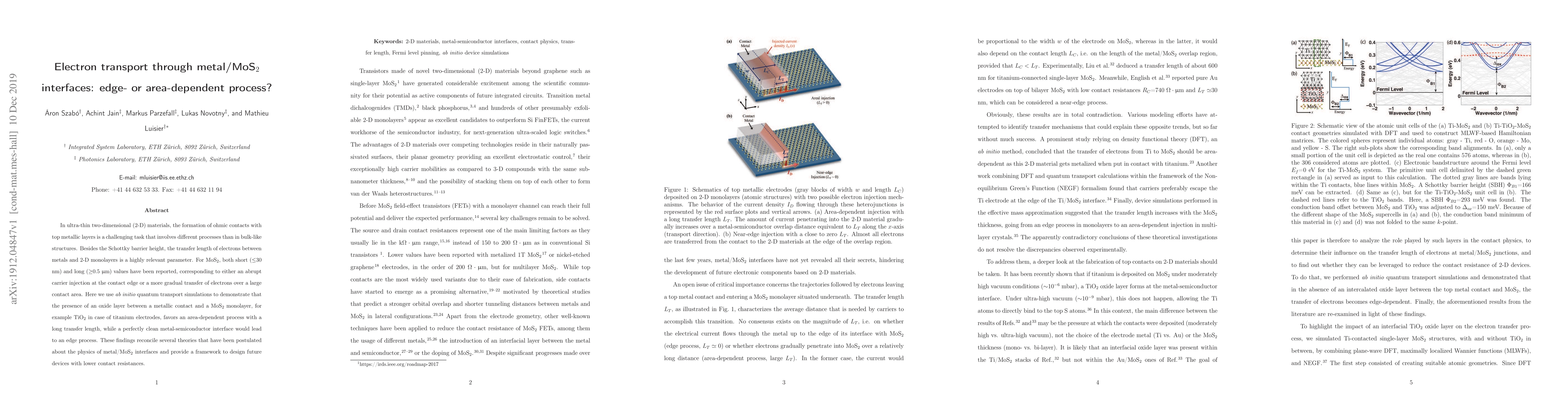
In ultra-thin two-dimensional (2-D) materials, the formation of ohmic contacts with top metallic layers is a challenging task that involves different processes than in bulk-like structures. Besides ...
Analogous to radio- and microwave antennas, optical nanoantennas are devices that receive and emit radiation at optical frequencies. Until recently, the realization of electrically driven optical an...
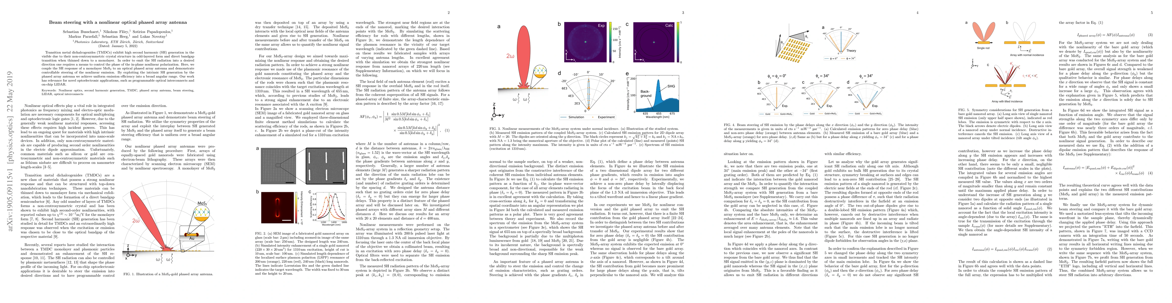
Transition metal dichalcogenides (TMDCs) exhibit high second harmonic (SH) generation in the visible due to their non-centrosymmetric crystal structure in odd-layered form and direct bandgap transit...
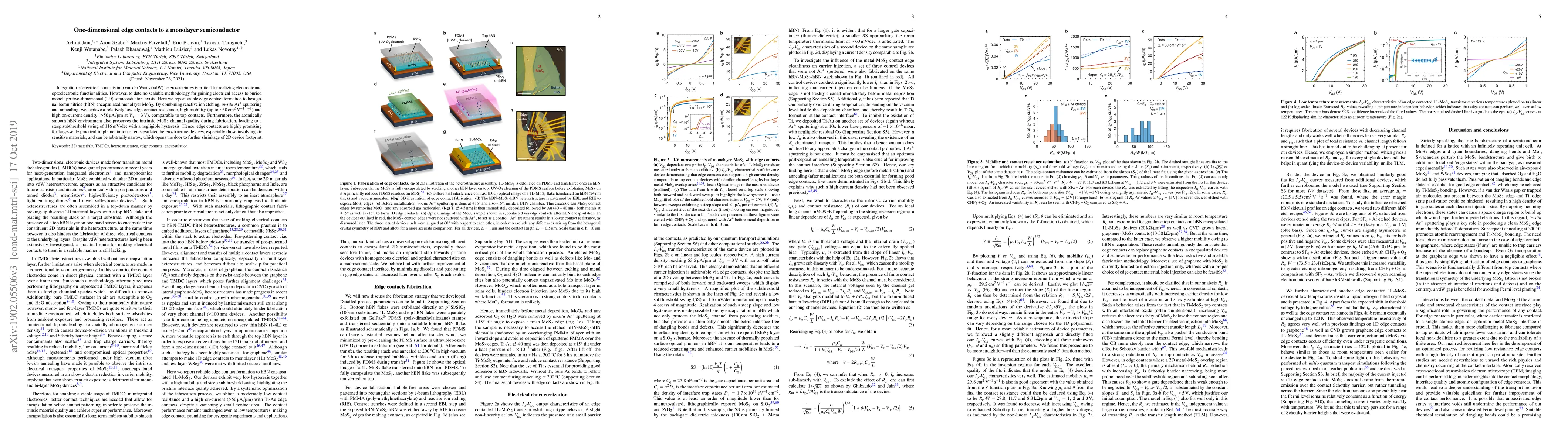
Integration of electrical contacts into van der Waals (vdW) heterostructures is critical for realizing electronic and optoelectronic functionalities. However, to date no scalable methodology for gai...