ArxivLens
M
Researcher

Martin Schalk

6 papers on arXiv

6 arXiv Papers
6 Total Publications
Profile

Academic Profile

Name M. Schalk
Total Papers 6
Scholar Profile View on Semantic Scholar
Metrics

Statistics

6 arXiv Papers
6 Total Publications
Publications

Papers on arXiv

Thumbnail for Three-dimensional magnetic resonance tomography with sub-10 nanometer
  resolution
arXiv
Three-dimensional magnetic resonance tomography with sub-10 nanometer resolution

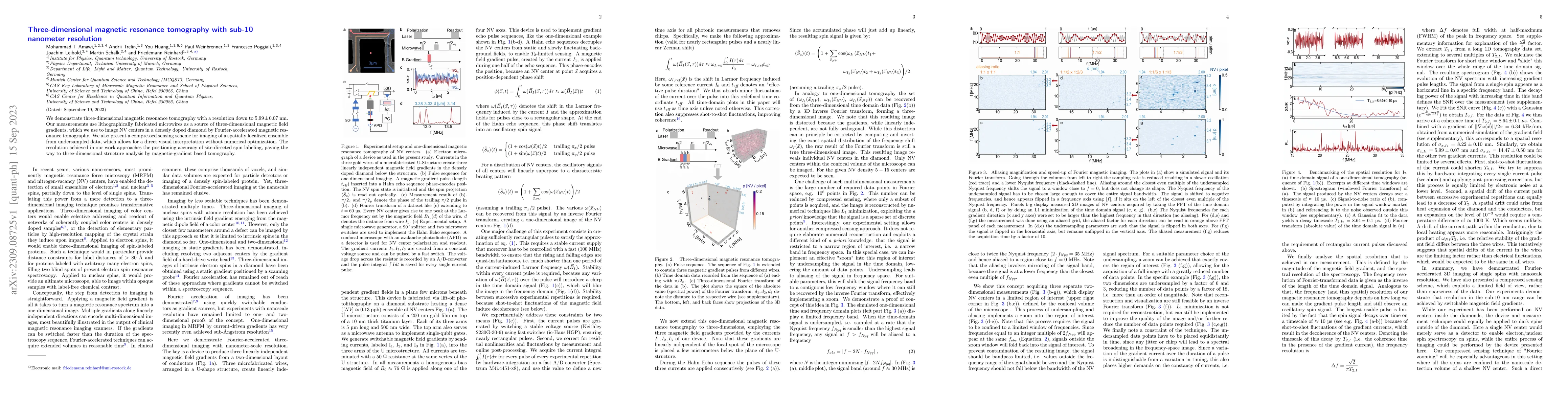
We demonstrate three-dimensional magnetic resonance tomography with a resolution down to 5.99 +- 0.07 nm. Our measurements use lithographically fabricated microwires as a source of three-dimensional...

Thumbnail for Extending the coherence time of spin defects in hBN enables advanced
  qubit control and quantum sensing
arXiv
Extending the coherence time of spin defects in hBN enables advanced qubit control and quantum sensing

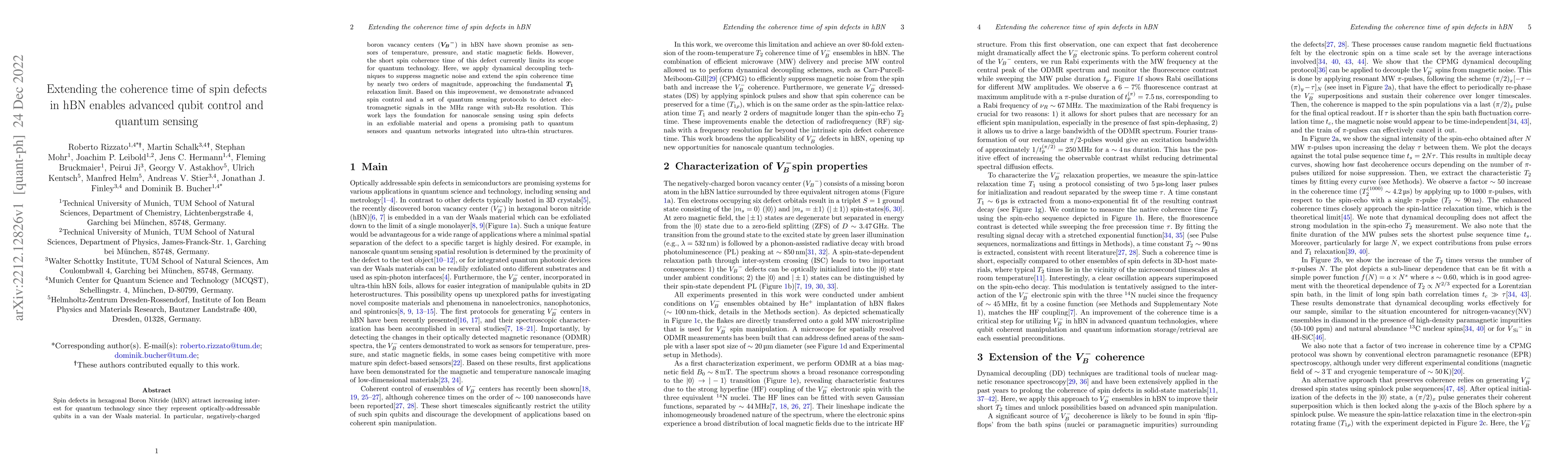
Spin defects in hexagonal Boron Nitride (hBN) attract increasing interest for quantum technology since they represent optically-addressable qubits in a van der Waals material. In particular, negativ...

Thumbnail for Emitter-Optomechanical Interaction in Ultra-High-Q hBN Nanocavities
arXiv
Emitter-Optomechanical Interaction in Ultra-High-Q hBN Nanocavities

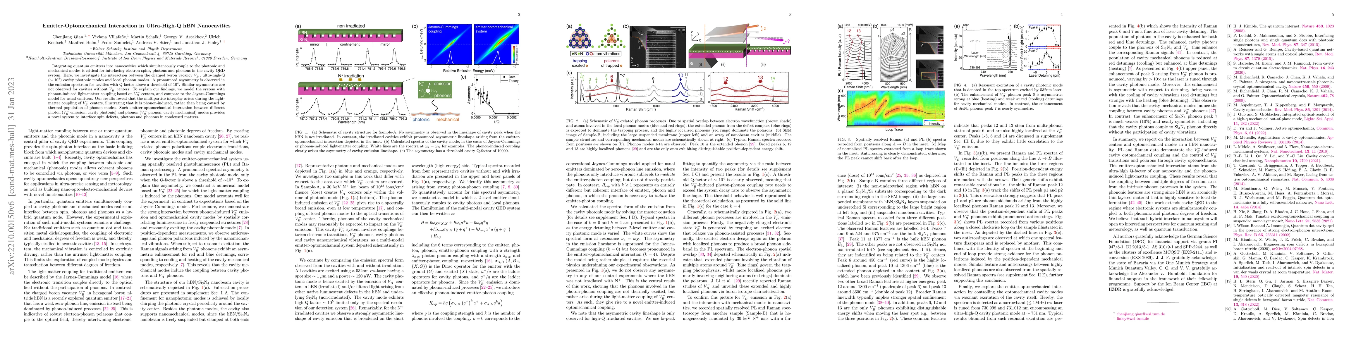
Integrating quantum emitters into nanocavities which simultaneously couple to the photonic and mechanical modes is critical for interfacing electron spins, photons and phonons in the cavity QED syst...

Thumbnail for The quantum dynamic range of room temperature spin imaging
arXiv
The quantum dynamic range of room temperature spin imaging

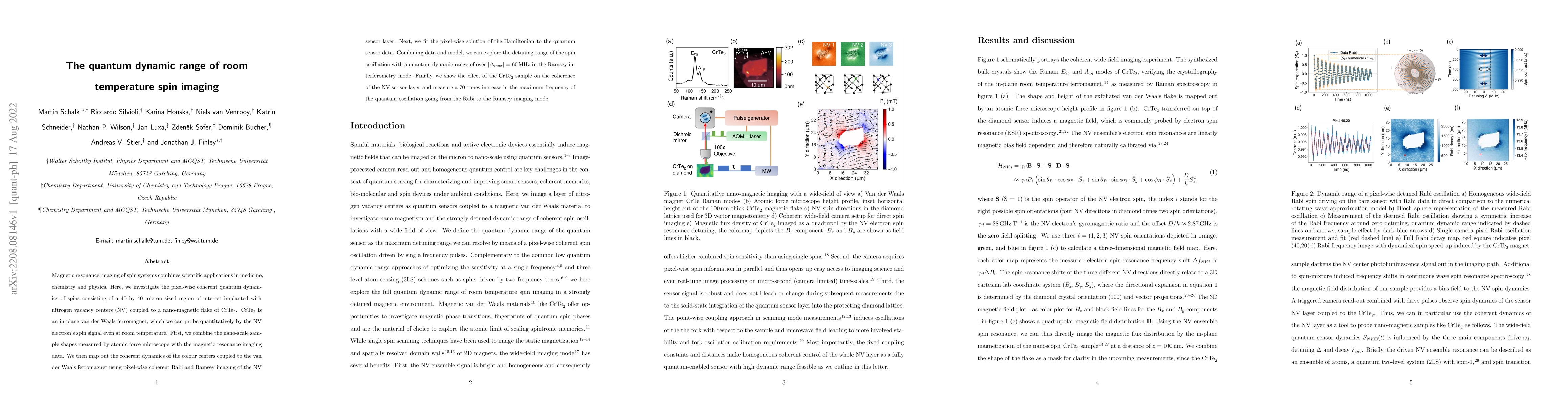
Magnetic resonance imaging of spin systems combines scientific applications in medicine, chemistry and physics. Here, we investigate the pixel-wise coherent quantum dynamics of spins consisting of a...

Thumbnail for Unveiling the Zero-Phonon Line of the Boron Vacancy Center by Cavity
  Enhanced Emission
arXiv
Unveiling the Zero-Phonon Line of the Boron Vacancy Center by Cavity Enhanced Emission

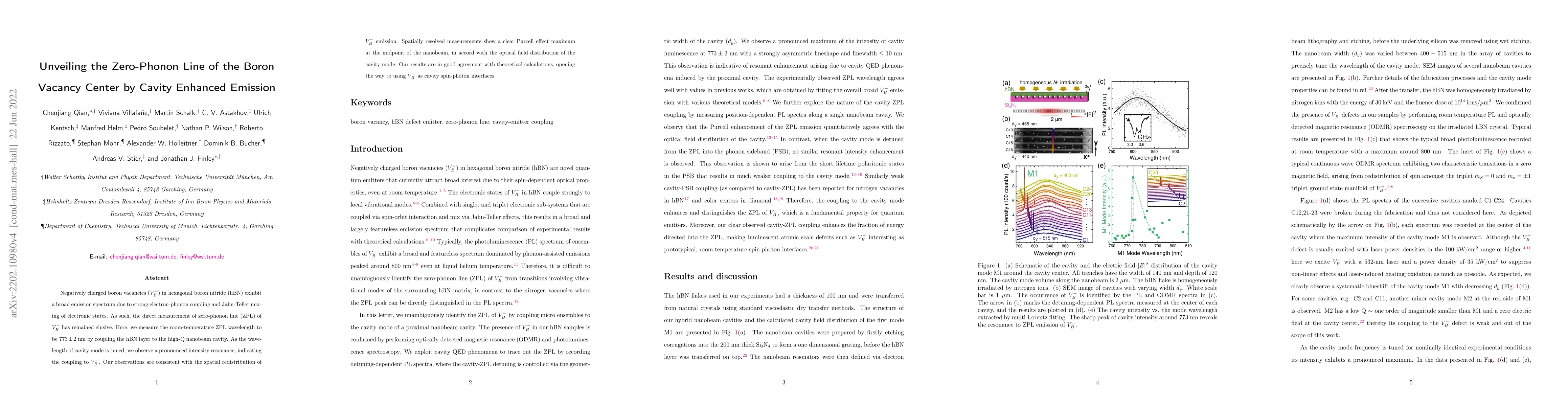
Negatively charged boron vacancies ($V_B^-$) in hexagonal boron nitride (hBN) exhibit a broad emission spectrum due to strong electron-phonon coupling and Jahn-Teller mixing of electronic states. As...

Thumbnail for Atomically Flat Dielectric Patterns for Band Gap Engineering and Lateral
  Junction Formation in MoSe$_2$ Monolayers
arXiv
Atomically Flat Dielectric Patterns for Band Gap Engineering and Lateral Junction Formation in MoSe$_2$ Monolayers

Combining a precise sputter etching method with subsequent AlO$_x$ growth within an atomic layer deposition chamber enables fabrication of atomically flat lateral patterns of SiO$_2$ and AlO$_x$. The ...

This website uses cookies to ensure you get the best experience. Learn more