Academic Profile
Statistics
Similar Authors
Papers on arXiv
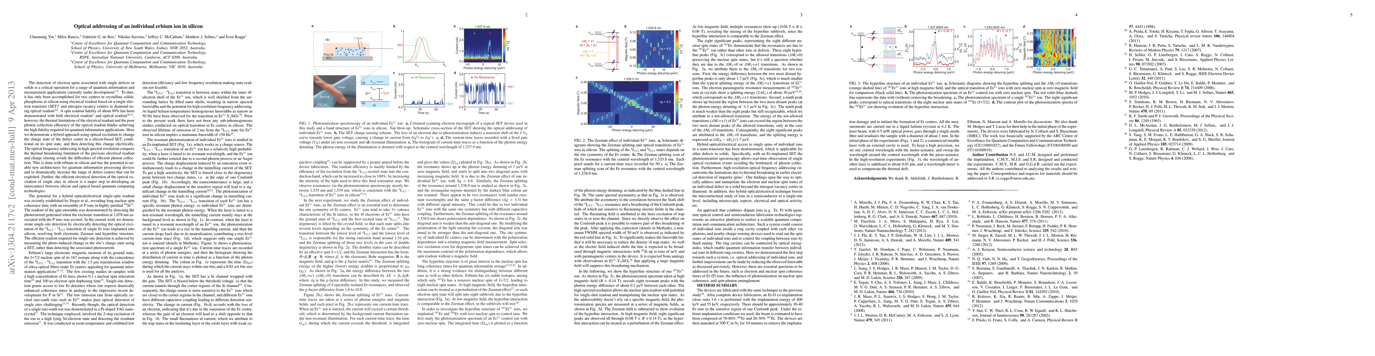
The detection of electron spins associated with single defects in solids is a critical operation for a range of quantum information and measurement applications currently under development. To date,...
Spins in silicon that are accessible via a telecom-compatible optical transition are a versatile platform for quantum information processing that can leverage the well-established silicon nanofabric...
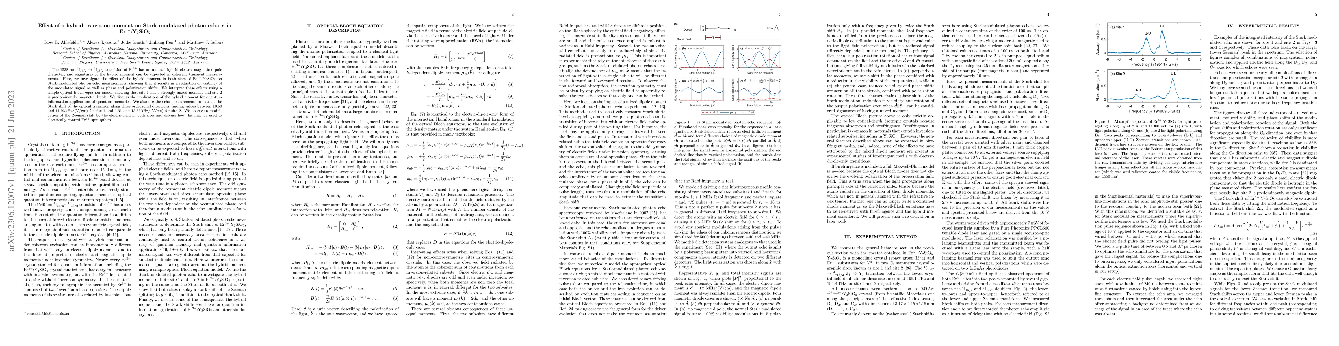
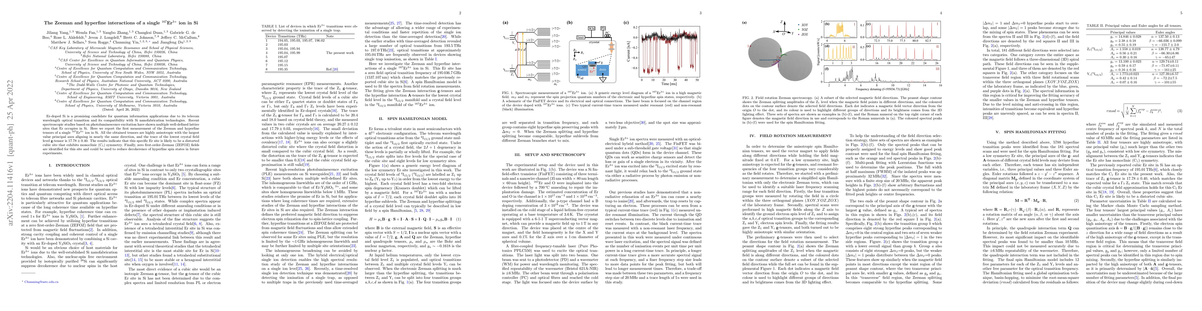
The 1538 nm ${}^4$I$_{15/2}$ - ${}^4$I$_{13/2}$ transition of Er$^{3+}$ has an unusual hybrid electric-magnetic dipole character, and signatures of the hybrid moment can be expected in coherent tran...
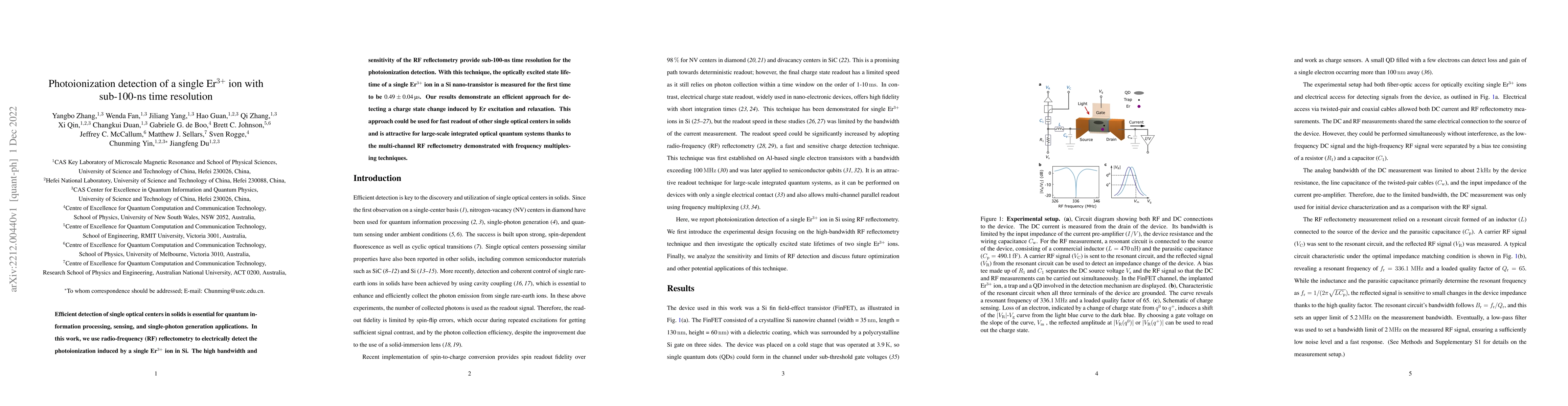
Efficient detection of single optical centers in solids is essential for quantum information processing, sensing, and single-photon generation applications. In this work, we use radio-frequency (RF)...
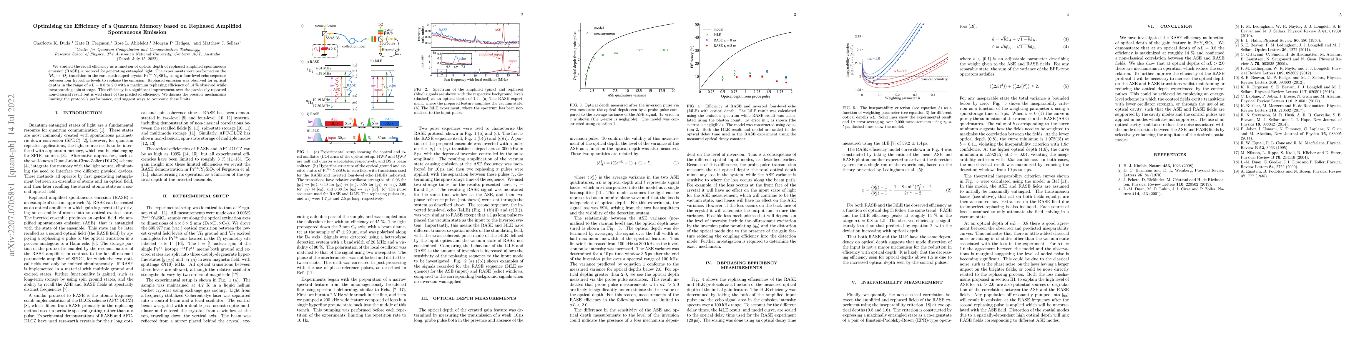
We studied the recall efficiency as a function of optical depth of rephased amplified spontaneous emission (RASE), a protocol for generating entangled light. The experiments were performed on the $^...
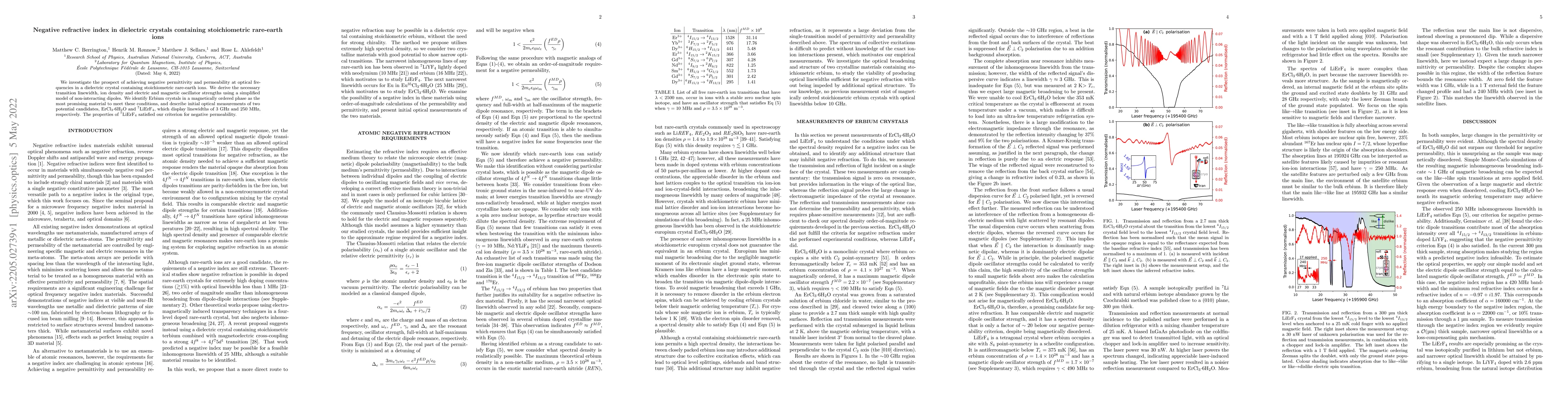
We investigate the prospect of achieving negative permittivity and permeability at optical frequencies in a dielectric crystal containing stoichiometric rare-earth ions. We derive the necessary tran...
Er-doped Si is a promising candidate for quantum information applications due to its telecom wavelength optical transition and its compatibility with Si nanofabrication technologies. Recent spectros...
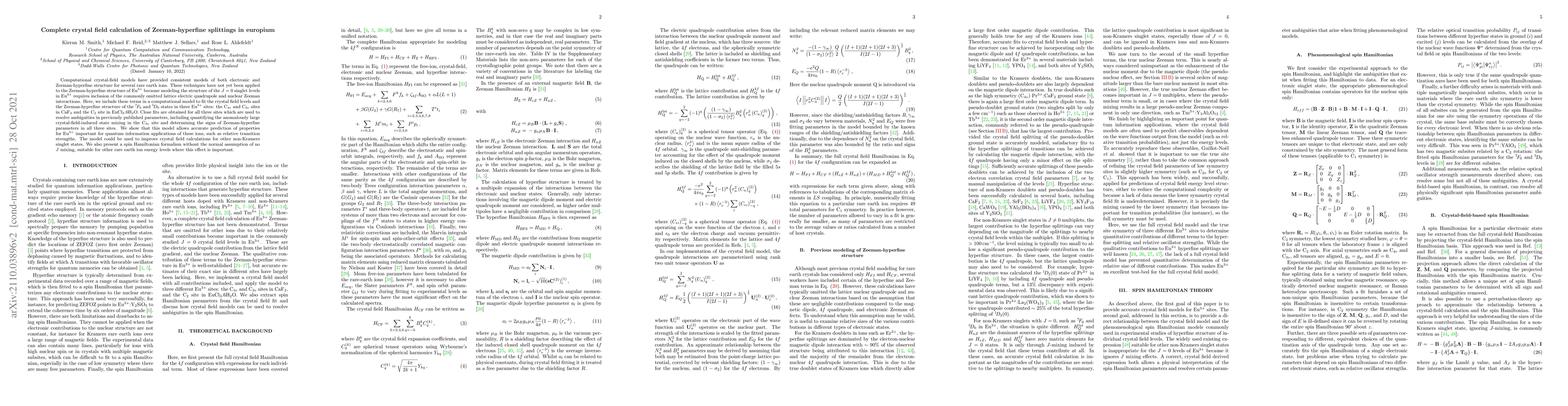
Computational crystal-field models have provided consistent models of both electronic and Zeeman-hyperfine structure for several rare earth ions. These techniques have not yet been applied to the Ze...
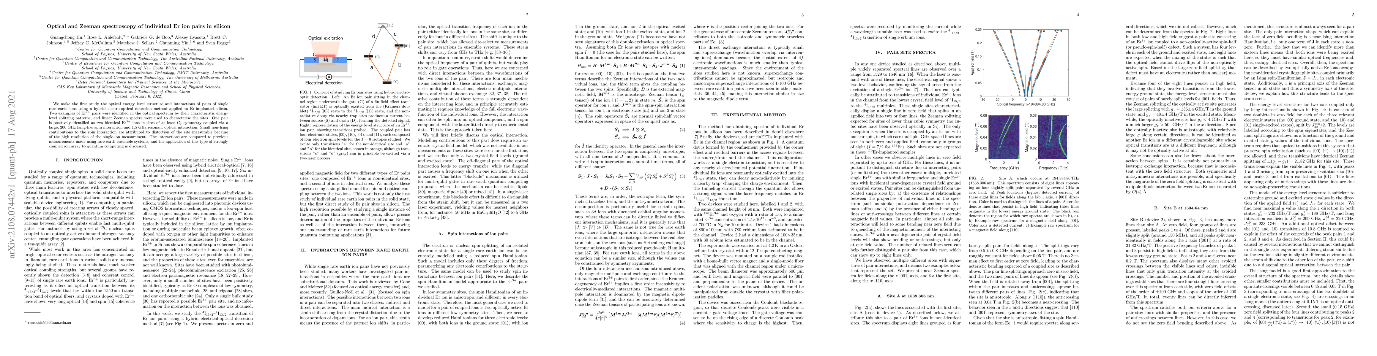
We make the first study the optical energy level structure and interactions of pairs of single rare earth ions using a hybrid electro-optical detection method applied to Er-implanted silicon. Two ex...
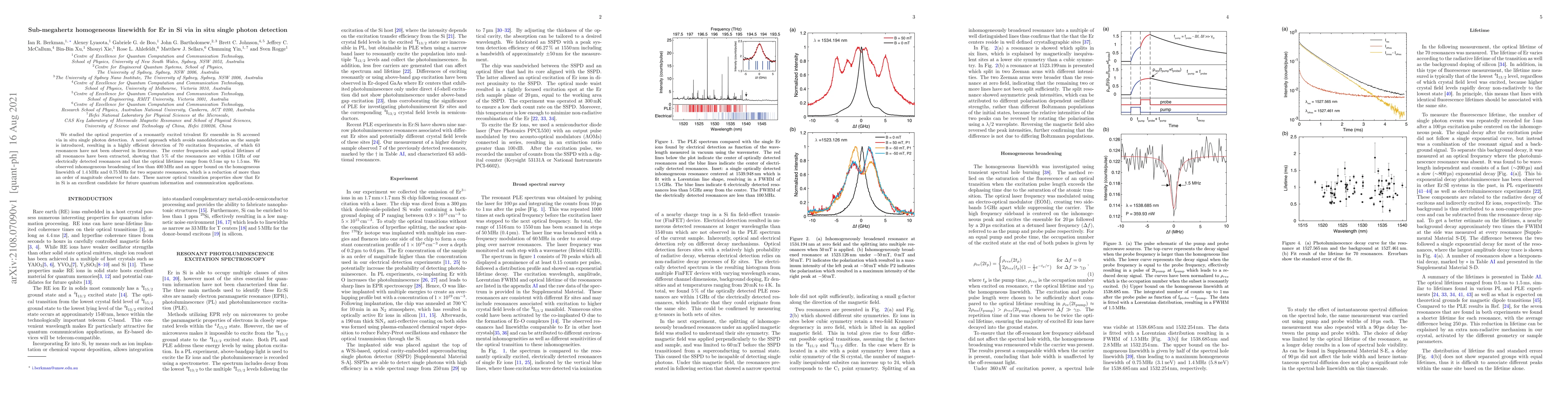
We studied the optical properties of a resonantly excited trivalent Er ensemble in Si accessed via in situ single photon detection. A novel approach which avoids nanofabrication on the sample is int...
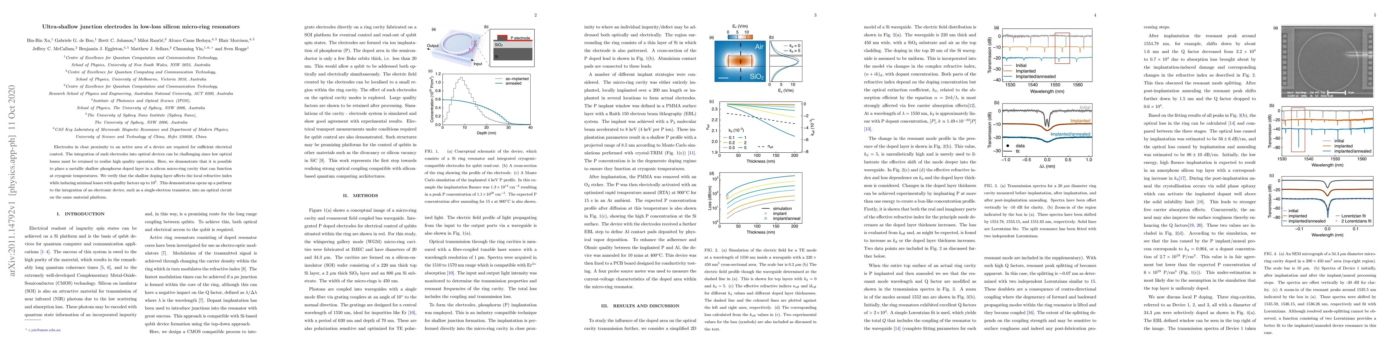
Electrodes in close proximity to an active area of a device are required for sufficient electrical control. The integration of such electrodes into optical devices can be challenging since low optic...
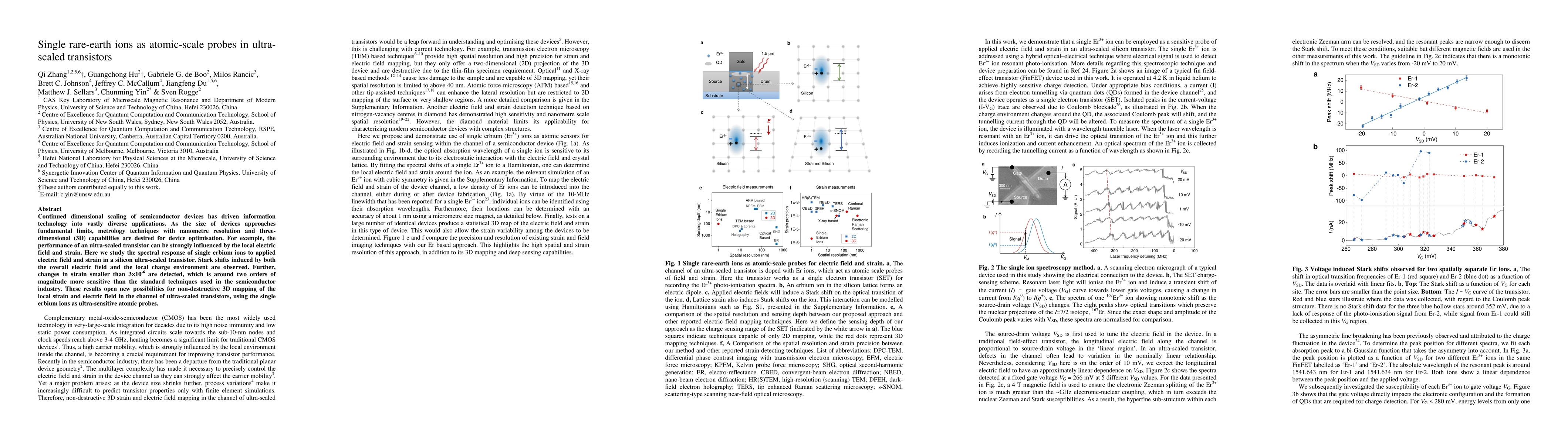
Continued dimensional scaling of semiconductor devices has driven information technology into vastly diverse applications. As the size of devices approaches fundamental limits, metrology techniques ...