Mauricio Terrones

34 papers on arXiv

Academic Profile

Name: M. Terrones
Total Papers: 13

Statistics

arXiv Papers 34
Total Publications 13

Papers on arXiv

Thumbnail for Strong magneto-optical responses of an ensemble of defect-bound excitons
  in aged WS$_{2}$ and WSe$_{2}$ monolayers

Strong magneto-optical responses of an ensemble of defect-bound excitons in aged WS$_{2}$ and WSe$_{2}$ monolayers

Transition metal dichalcogenide (TMD) monolayers present a singular coupling in their spin and valley degrees of freedom. Moreover, by applying an external magnetic field it is possible to break the...

Thumbnail for Phonon and exciton temperature-dependent properties of twisted MoS$_2$

Phonon and exciton temperature-dependent properties of twisted MoS$_2$

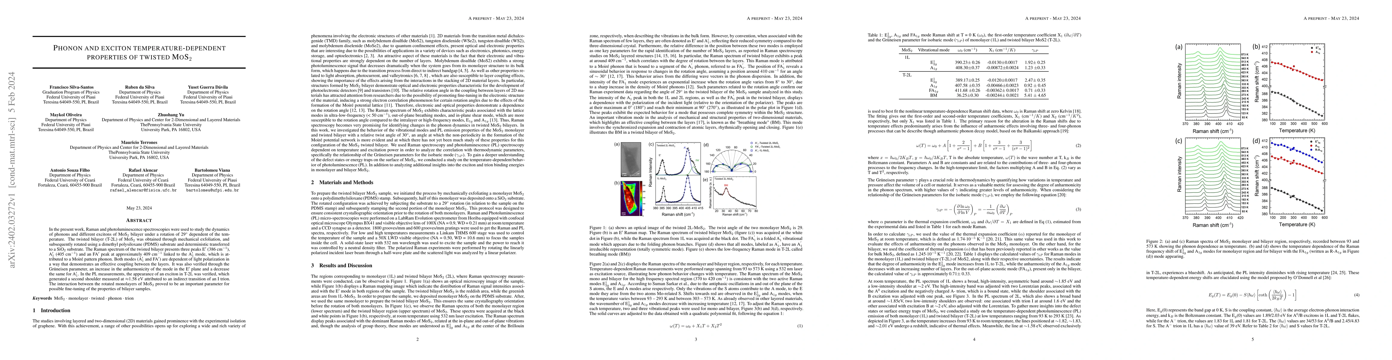
In the present work, Raman and photoluminescence spectroscopies were used to study the dynamics of phonons and different excitons of MoS$_2$ bilayer under a rotation of 29$^{\circ}$ dependent of the...

Thumbnail for Vanadium-Doped Molybdenum Disulfide Monolayers with Tunable Electronic
  and Magnetic Properties: Do Vanadium-Vacancy Pairs Matter?

Vanadium-Doped Molybdenum Disulfide Monolayers with Tunable Electronic and Magnetic Properties: Do Vanadium-Vacancy Pairs Matter?

Monolayers of molybdenum disulfide (MoS2) are the most studied two-dimensional (2D) transition-metal dichalcogenides (TMDs), due to its exceptional optical, electronic, and opto-electronic propertie...

Thumbnail for Effects of Vanadium Doping on the Optical Response and Electronic
  Structure of WS$_{2}$ Monolayers

Effects of Vanadium Doping on the Optical Response and Electronic Structure of WS$_{2}$ Monolayers

Two-dimensional dilute magnetic semiconductors has been recently reported in semiconducting transition metal dichalcogenides by the introduction of spin-polarized transition metal atoms as dopants. ...

Thumbnail for A substitutional quantum defect in WS$_2$ discovered by high-throughput
  computational screening and fabricated by site-selective STM manipulation

A substitutional quantum defect in WS$_2$ discovered by high-throughput computational screening and fabricated by site-selective STM manipulation

Point defects in two-dimensional materials are of key interest for quantum information science. However, the space of possible defects is immense, making the identification of high-performance quant...

Thumbnail for Sulfur Vacancy Related Optical Transitions in Graded Alloys of MoxW1-xS2
  Monolayers

Sulfur Vacancy Related Optical Transitions in Graded Alloys of MoxW1-xS2 Monolayers

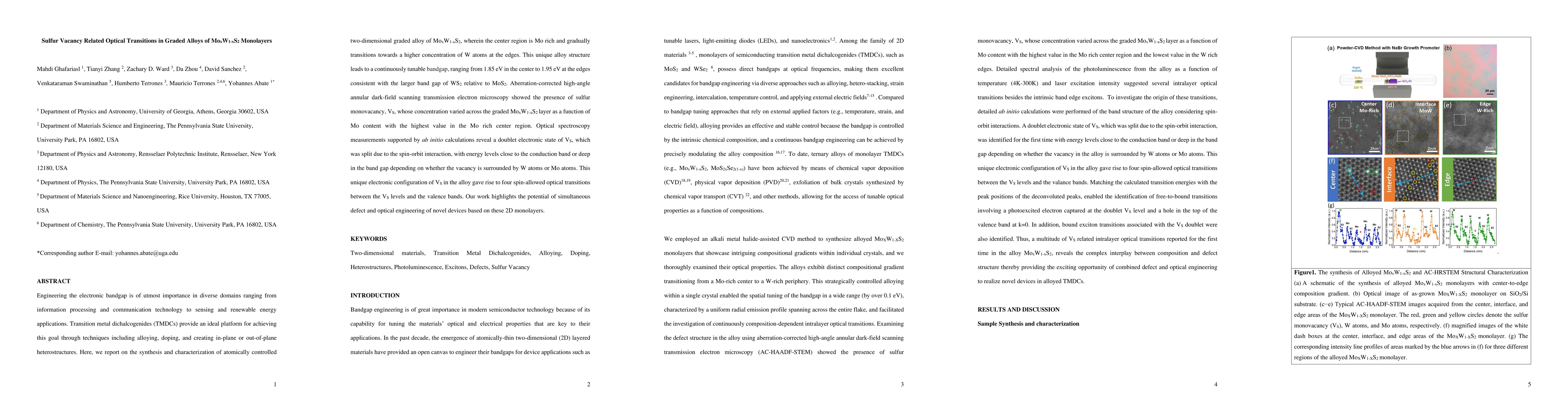
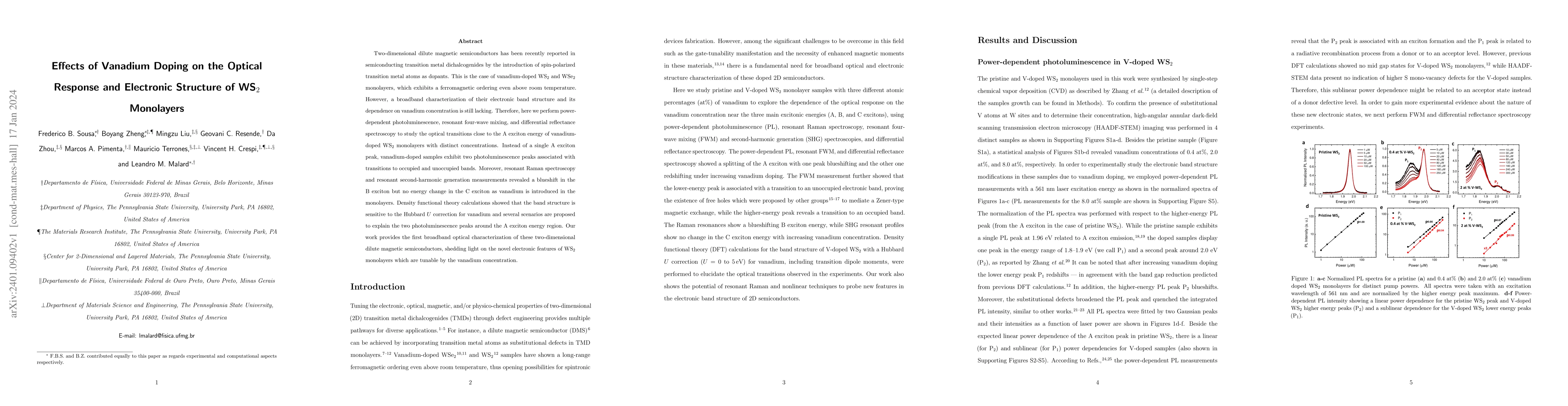
Engineering the electronic bandgap is of utmost importance in diverse domains ranging from information processing and communication technology to sensing and renewable energy applications. Transitio...

Thumbnail for WS$_2$ Band Gap Renormalization Induced by Tomonaga Luttinger Liquid
  Formation in Mirror Twin Boundaries

WS$_2$ Band Gap Renormalization Induced by Tomonaga Luttinger Liquid Formation in Mirror Twin Boundaries

Tomonaga-Luttinger liquid (TLL) behavior in one-dimensional systems has been predicted and shown to occur at semiconductor-to-metal transitions within two-dimensional materials. Reports of mirror tw...

Thumbnail for Light-driven C-H bond activation mediated by 2D transition metal
  dichalcogenides

Light-driven C-H bond activation mediated by 2D transition metal dichalcogenides

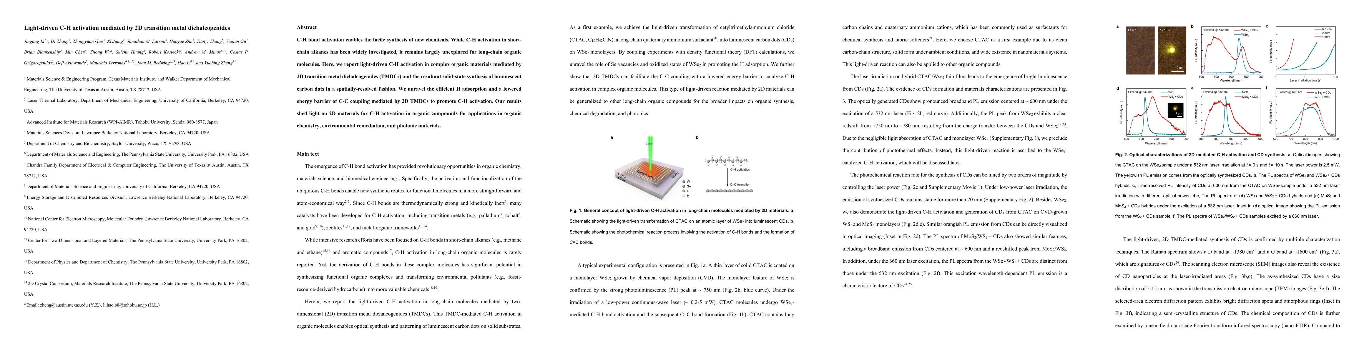
C-H bond activation enables the facile synthesis of new chemicals. While C-H activation in short-chain alkanes has been widely investigated, it remains largely unexplored for long-chain organic mole...

Thumbnail for Accurate Virus Identification with Interpretable Raman Signatures by
  Machine Learning

Accurate Virus Identification with Interpretable Raman Signatures by Machine Learning

Rapid identification of newly emerging or circulating viruses is an important first step toward managing the public health response to potential outbreaks. A portable virus capture device coupled wi...

Thumbnail for Autonomous Investigations over WS$_2$ and Au{111} with Scanning Probe
  Microscopy

Autonomous Investigations over WS$_2$ and Au{111} with Scanning Probe Microscopy

Individual atomic defects in 2D materials impact their macroscopic functionality. Correlating the interplay is challenging, however, intelligent hyperspectral scanning tunneling spectroscopy (STS) m...

Thumbnail for Trends on 3d Transition Metal Coordination on Monolayer MoS$_2$

Trends on 3d Transition Metal Coordination on Monolayer MoS$_2$

Two-dimensional materials (2DM) have attracted much interest due to their distinct optical, electronic, and catalytic properties. These properties can be by tuned a range of methods including substi...

Thumbnail for Second- and third-order optical susceptibilities in bidimensional
  semiconductors near excitons states

Second- and third-order optical susceptibilities in bidimensional semiconductors near excitons states

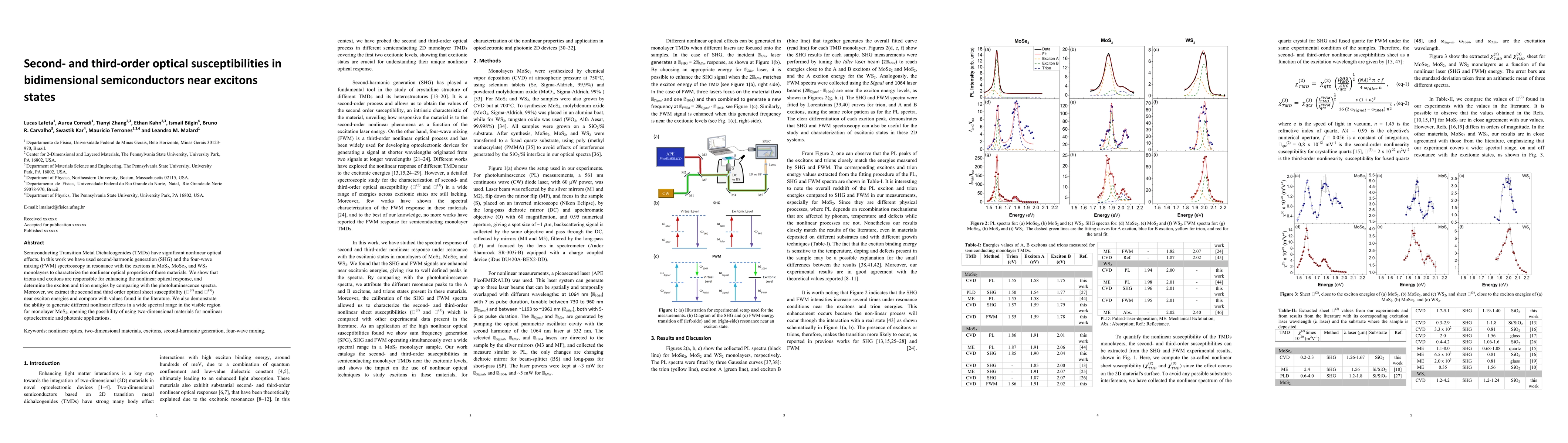
Semiconducting Transition Metal Dichalcogenides (TMDs) have significant nonlinear optical effects. In this work we have used second-harmonic generation (SHG) and the four-wave mixing (FWM) spectrosc...

Thumbnail for Directivity modulation of exciton emission using single dielectric
  nanospheres

Directivity modulation of exciton emission using single dielectric nanospheres

Coupling emitters with nanoresonators is an effective strategy to control light emission at the subwavelength scale with high efficiency. Low-loss dielectric nanoantennas hold particular promise for...

Thumbnail for Vibronic response of a spin-1/2 state from a carbon impurity in
  two-dimensional WS$_2$

Vibronic response of a spin-1/2 state from a carbon impurity in two-dimensional WS$_2$

We demonstrate the creation of a spin-1/2 state via the atomically controlled generation of magnetic carbon radical ions (CRIs) in synthetic two-dimensional transition metal dichalcogenides (TMDs). ...

Thumbnail for Impact of 150keV and 590keV proton irradiation on monolayer MoS2

Impact of 150keV and 590keV proton irradiation on monolayer MoS2

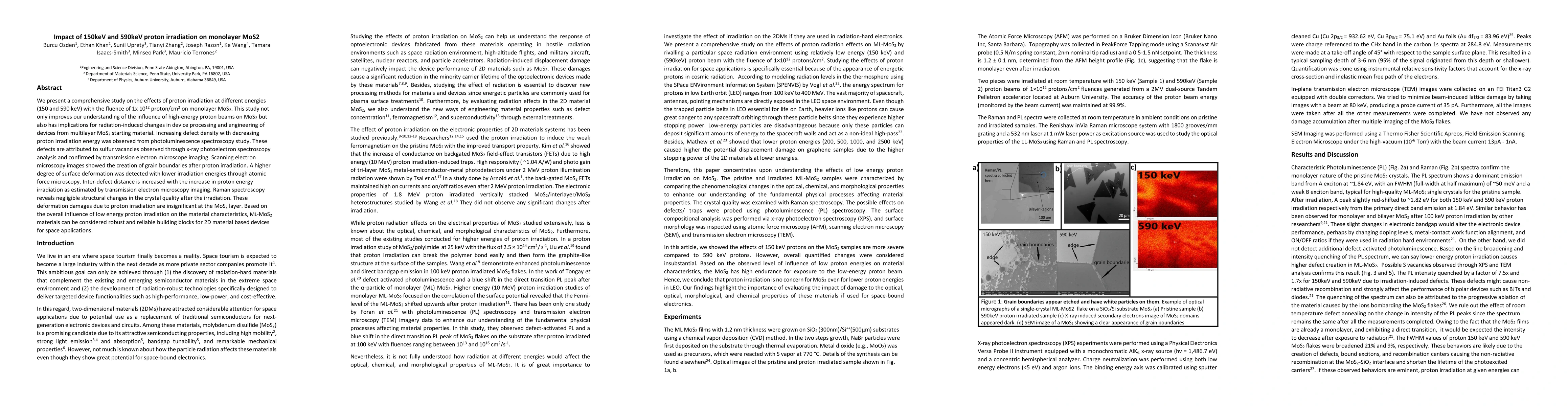
We present a comprehensive study on the effects of proton irradiation at different energies (150 and 590 keV) with the fluence of 1x 10¹² proton/cm2 on monolayer MoS2. This study not only improves o...

Thumbnail for Light-controlled room temperature ferromagnetism in vanadium-doped
  tungsten diselenide semiconducting monolayers

Light-controlled room temperature ferromagnetism in vanadium-doped tungsten diselenide semiconducting monolayers

Atomically thin transition metal dichalcogenide (TMD) semiconductors hold enormous potential for modern optoelectronic devices and quantum computing applications. By inducing long-range ferromagneti...

Thumbnail for Wafer-scale epitaxial growth of single orientation WS2 monolayers on
  sapphire

Wafer-scale epitaxial growth of single orientation WS2 monolayers on sapphire

Realization of wafer-scale single-crystal films of transition metal dichalcogenides (TMDs) such as tungsten sulfide requires epitaxial growth and coalescence of oriented domains to form a continuous...

Thumbnail for Photo-degradation Protection in 2D In-Plane Heterostructures Revealed by
  Hyperspectral Nanoimaging: the Role of Nano-Interface 2D Alloys

Photo-degradation Protection in 2D In-Plane Heterostructures Revealed by Hyperspectral Nanoimaging: the Role of Nano-Interface 2D Alloys

Single-layer heterostructures exhibit striking quasiparticle properties and many-body interaction effects that hold promise for a range of applications. However, their properties can be altered by i...

Thumbnail for Monolayer Vanadium-doped Tungsten Disulfide: A Room-Temperature Dilute
  Magnetic Semiconductor

Monolayer Vanadium-doped Tungsten Disulfide: A Room-Temperature Dilute Magnetic Semiconductor

Dilute magnetic semiconductors, achieved through substitutional doping of spin-polarized transition metals into semiconducting systems, enable experimental modulation of spin dynamics in ways that h...

Thumbnail for Tunable Ferromagnetism and Thermally Induced Spin Flip in Vanadium-doped
  Tungsten Diselenide Monolayers at Room Temperature

Tunable Ferromagnetism and Thermally Induced Spin Flip in Vanadium-doped Tungsten Diselenide Monolayers at Room Temperature

The outstanding optoelectronic and valleytronic properties of transition metal dichalcogenides (TMDs) have triggered intense research efforts by the scientific community. An alternative to induce lo...

Thumbnail for On the origin of non-classical ripples in draped graphene sheets

On the origin of non-classical ripples in draped graphene sheets

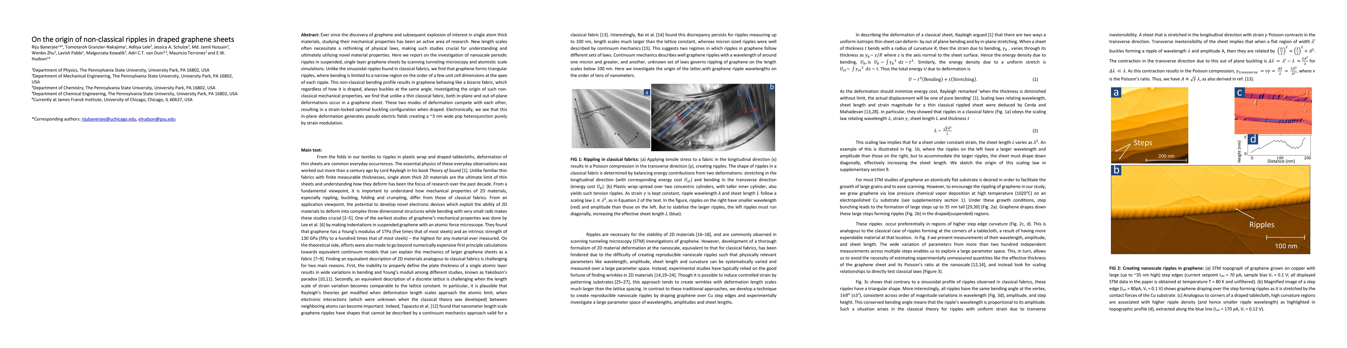
Ever since the discovery of graphene and subsequent explosion of interest in single atom thick materials, studying their mechanical properties has been an active area of research. New length scales ...

Thumbnail for Nanoscale patterning of quasiparticle band alignment

Nanoscale patterning of quasiparticle band alignment

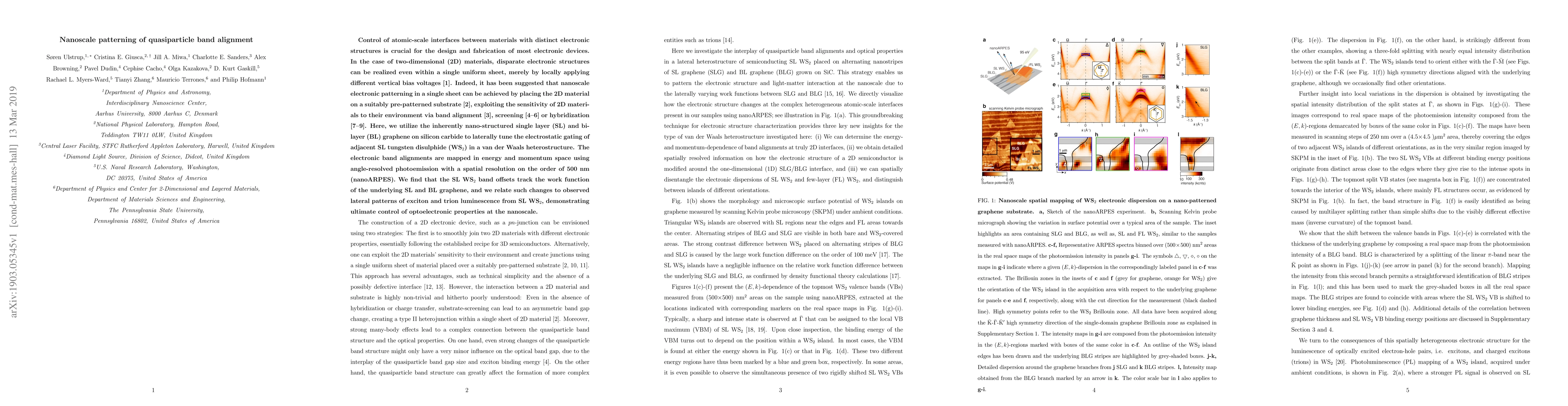
Control of atomic-scale interfaces between materials with distinct electronic structures is crucial for the design and fabrication of most electronic devices. In the case of two-dimensional (2D) mat...

Thumbnail for Nonlinear dark-field imaging of 1D defects in monolayer dichalcogenides

Nonlinear dark-field imaging of 1D defects in monolayer dichalcogenides

Extended defects with one dimensionality smaller than that of the host, such as 2D grain boundaries in 3D materials or 1D grain boundaries in 2D materials, can be particularly damaging since they di...

Thumbnail for Downscaling of non van der Waals Semimetallic W5N6 with Resistivity
  Preservation

Downscaling of non van der Waals Semimetallic W5N6 with Resistivity Preservation

The bulk phase of transition metal nitrides (TMNs) has long been a subject of extensive investigation due to their utility as coating materials, electrocatalysts, and diffusion barriers, attributed to...

Thumbnail for Enhancement of Second Harmonic Generation in Monolayer WS2 by
  Feedback-Based Wavefront Shaping

Enhancement of Second Harmonic Generation in Monolayer WS2 by Feedback-Based Wavefront Shaping

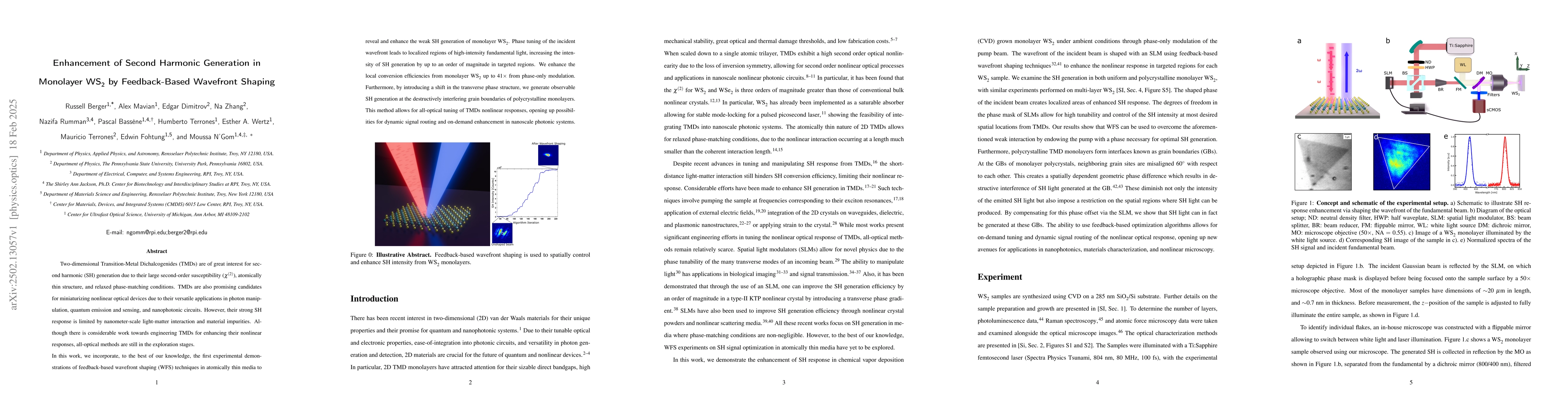
Two-dimensional Transition-Metal Dichalcogenides (TMDs) are of great interest for second harmonic (SH) generation due to their large second-order susceptibility, atomically thin structure, and relaxed...

Thumbnail for A Universal Raman Spectroscopic Framework for Defect Quantification in
  Mono-to-Multilayer Graphenic Materials: The Graphene Atlas

A Universal Raman Spectroscopic Framework for Defect Quantification in Mono-to-Multilayer Graphenic Materials: The Graphene Atlas

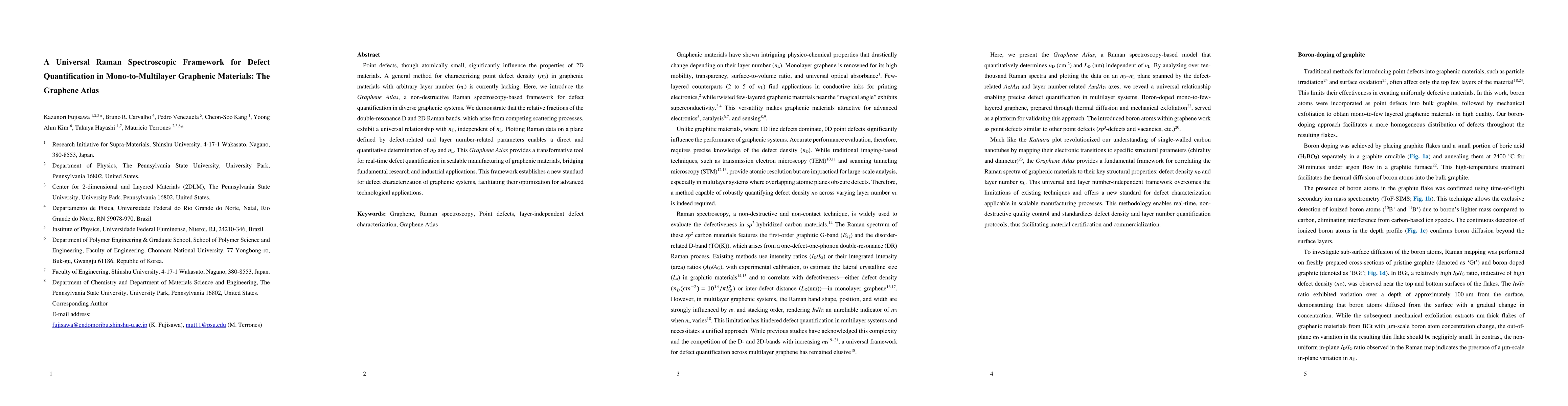
Point defects, though atomically small, significantly influence the properties of 2D materials. A general method for characterizing point defect density ($n_{ D }$) in graphenic materials with arbitra...

Thumbnail for Interface Magnetism in Vanadium-doped MoS$_2$/Graphene Heterostructures

Interface Magnetism in Vanadium-doped MoS$_2$/Graphene Heterostructures

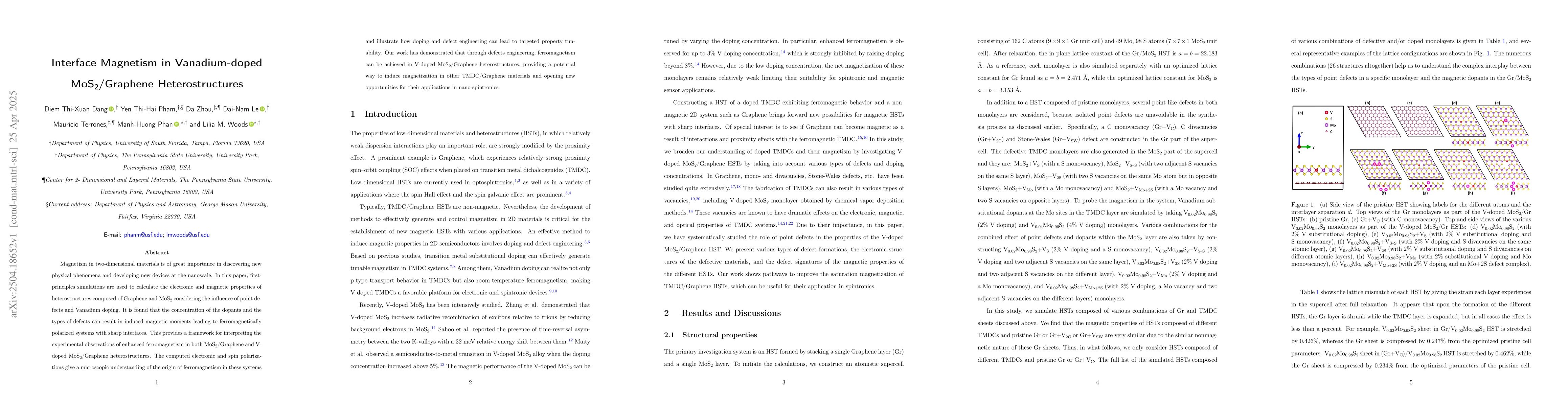
Magnetism in two-dimensional materials is of great importance in discovering new physical phenomena and developing new devices at the nanoscale. In this paper, first-principles simulations are used to...

Thumbnail for Roadmap for Photonics with 2D Materials

Roadmap for Photonics with 2D Materials

Triggered by the development of exfoliation and the identification of a wide range of extraordinary physical properties in self-standing films consisting of one or few atomic layers, two-dimensional (...

Thumbnail for Understanding and Controlling V-Doping and S-Vacancy Behavior in
  Two-Dimensional Semiconductors- Toward Predictive Design

Understanding and Controlling V-Doping and S-Vacancy Behavior in Two-Dimensional Semiconductors- Toward Predictive Design

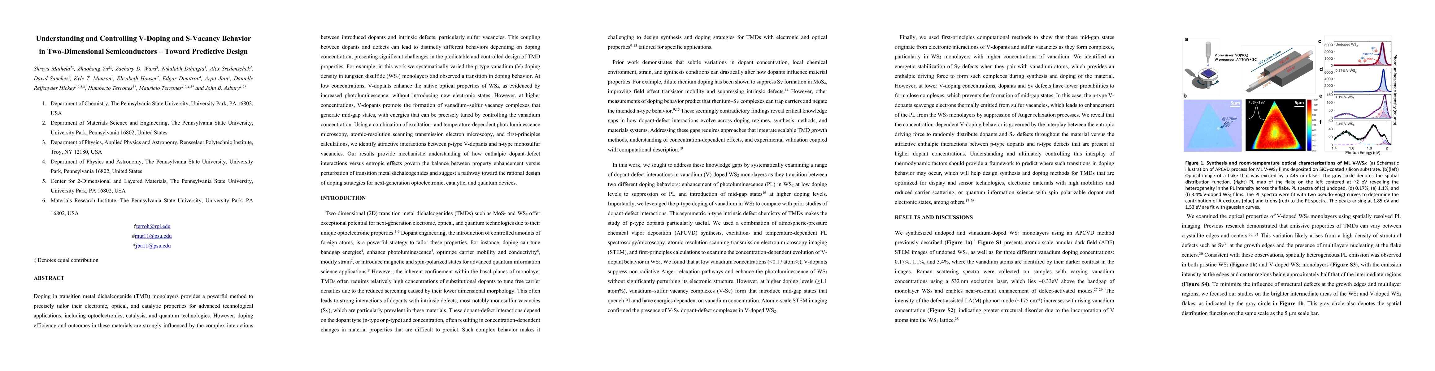
Doping in transition metal dichalcogenide (TMD) monolayers provides a powerful method to precisely tailor their electronic, optical, and catalytic properties for advanced technological applications, i...

Thumbnail for Machine Learning Integrated Near-Infrared Surface-Enhanced Raman
  Spectroscopy for Accurate Strain-Level Virus Identification

Machine Learning Integrated Near-Infrared Surface-Enhanced Raman Spectroscopy for Accurate Strain-Level Virus Identification

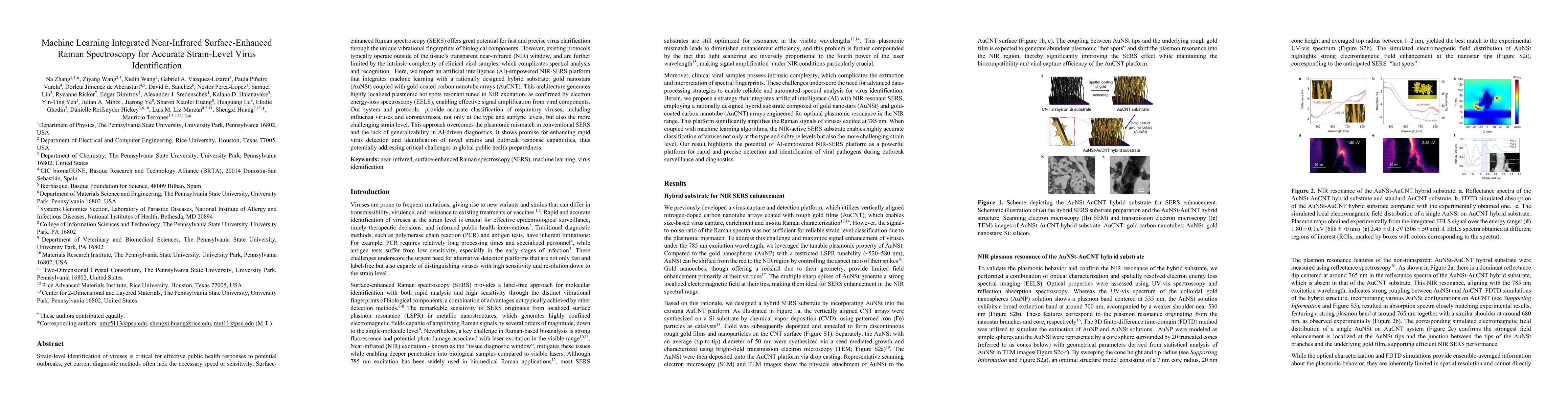
Strain-level identification of viruses is critical for effective public health responses to potential outbreaks, yet current diagnostic methods often lack the necessary speed or sensitivity. Surface-e...

Thumbnail for First principles and scanning tunneling spectroscopical evidences for
  thermodynamically stable "on-top" sulfur divacancy in monolayer WS$_{2}$

First principles and scanning tunneling spectroscopical evidences for thermodynamically stable "on-top" sulfur divacancy in monolayer WS$_{2}$

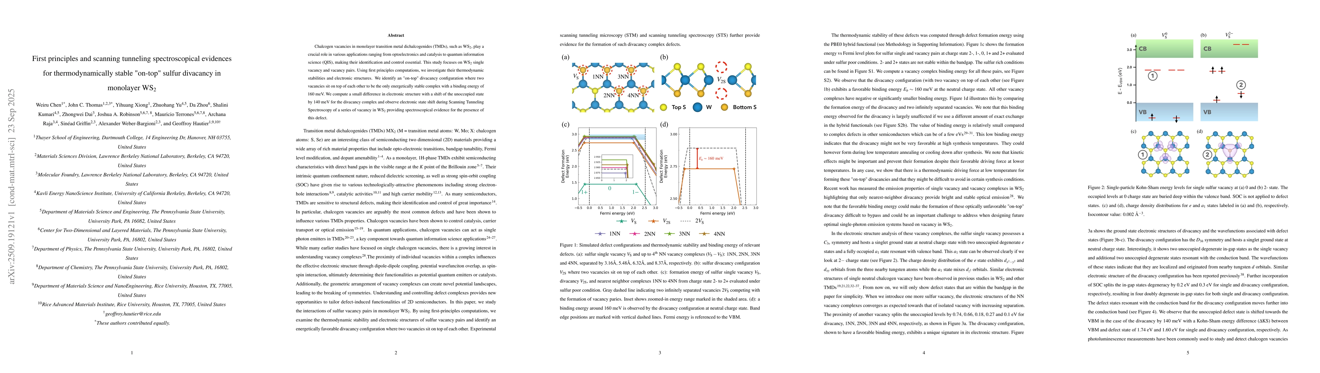
Chalcogen vacancies in monolayer transition metal dichalcogenides (TMDs), such as WS$_{2}$, play a crucial role in various applications ranging from optoelectronics and catalysis to quantum informatio...

Thumbnail for Nanoscopy of Excitons in Atomically Thin In-Plane Heterostructures with Nanointerfaces

Nanoscopy of Excitons in Atomically Thin In-Plane Heterostructures with Nanointerfaces

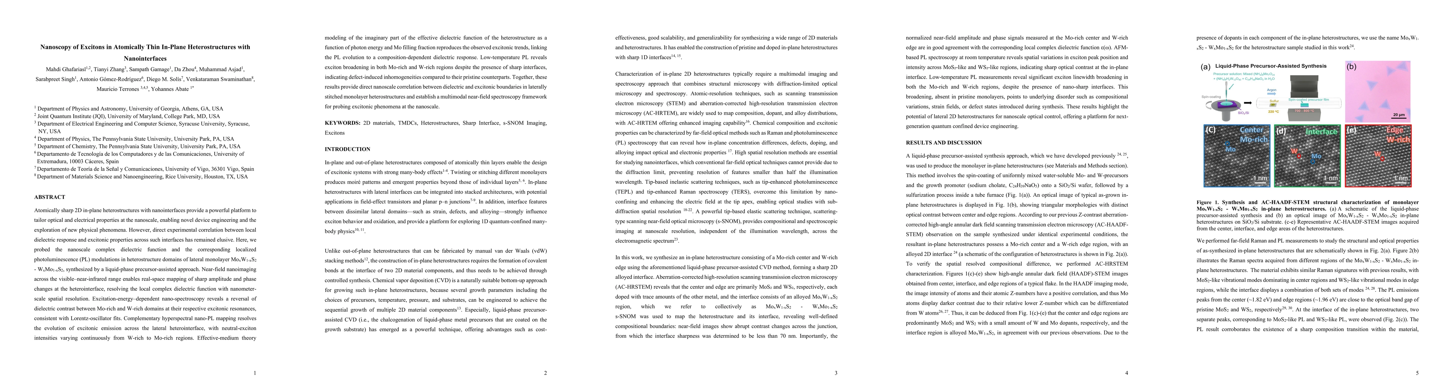
Atomically sharp 2D in-plane heterostructures with nanoscale interfaces provide a powerful platform for tailoring optical and electrical properties at the nanoscale, enabling novel device engineering ...

Thumbnail for Resonance-Enhanced Four-Wave Mixing Imaging for Mapping Defect Regions in Vanadium-Doped WS2 Monolayers

Resonance-Enhanced Four-Wave Mixing Imaging for Mapping Defect Regions in Vanadium-Doped WS2 Monolayers

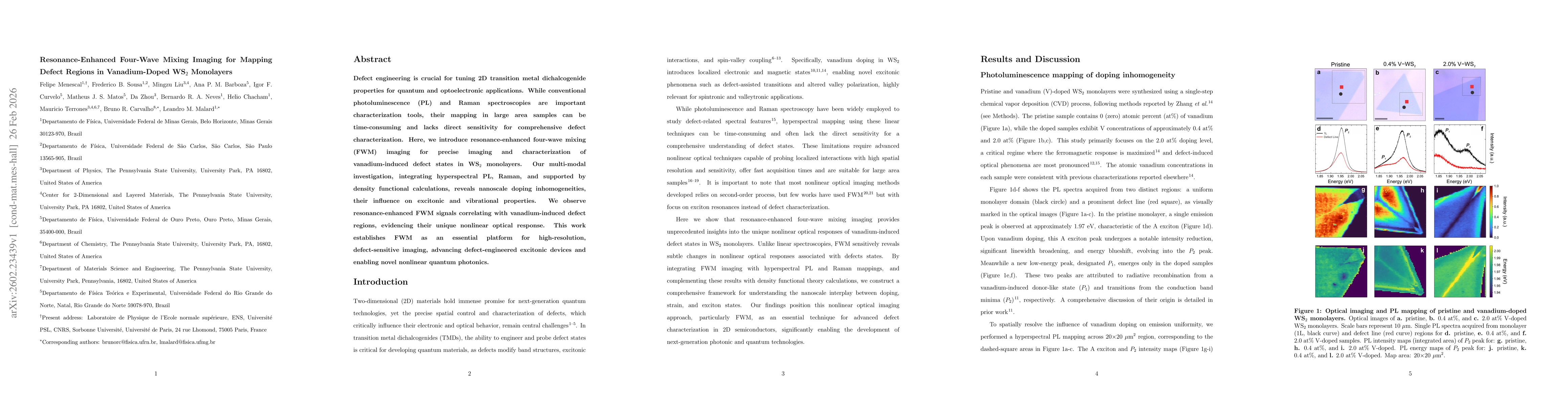
Defect engineering is crucial for tuning 2D transition metal dichalcogenide properties for quantum and optoelectronic applications. While conventional photoluminescence (PL) and Raman spectroscopies a...

Thumbnail for Anisotropic Dopant and Strain Architectures in WS$_2$ Nanocrystals Driven by Growth Kinetics

Anisotropic Dopant and Strain Architectures in WS$_2$ Nanocrystals Driven by Growth Kinetics

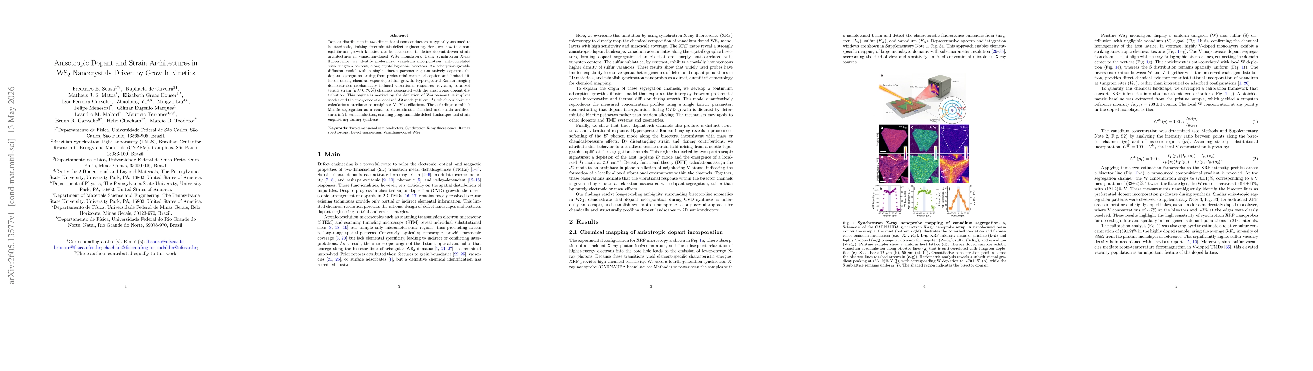
Dopant distribution in two-dimensional semiconductors is typically assumed to be stochastic, limiting deterministic defect engineering. Here, we show that non-equilibrium growth kinetics can be harnes...

This website uses cookies to ensure you get the best experience. Learn more