ArxivLens
M
Researcher

Max Bergmann

5 papers on arXiv

5 arXiv Papers
165 Total Publications
Profile

Academic Profile

Name M. Bergmann
Total Papers 165
Scholar Profile View on Semantic Scholar
Metrics

Statistics

5 arXiv Papers
165 Total Publications
Publications

Papers on arXiv

Thumbnail for Excitons in epitaxially grown WS2 on Graphene: a nanometer-resolved EELS
  and DFT study
arXiv
Excitons in epitaxially grown WS2 on Graphene: a nanometer-resolved EELS and DFT study

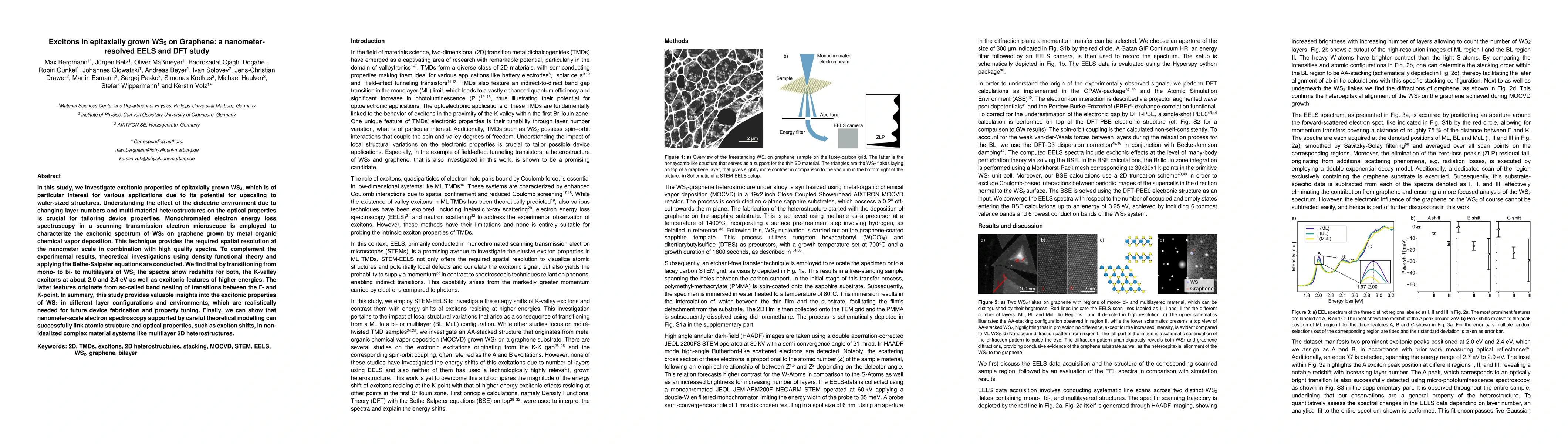
In this study, we investigate excitonic properties of epitaxially grown WS2, which is of particular interest for various applications due to its potential for upscaling to wafer sized structures. Un...

Thumbnail for A Small Step for Epitaxy, a Large Step Towards Twist Angle Control in 2D
  Heterostructures
arXiv
A Small Step for Epitaxy, a Large Step Towards Twist Angle Control in 2D Heterostructures

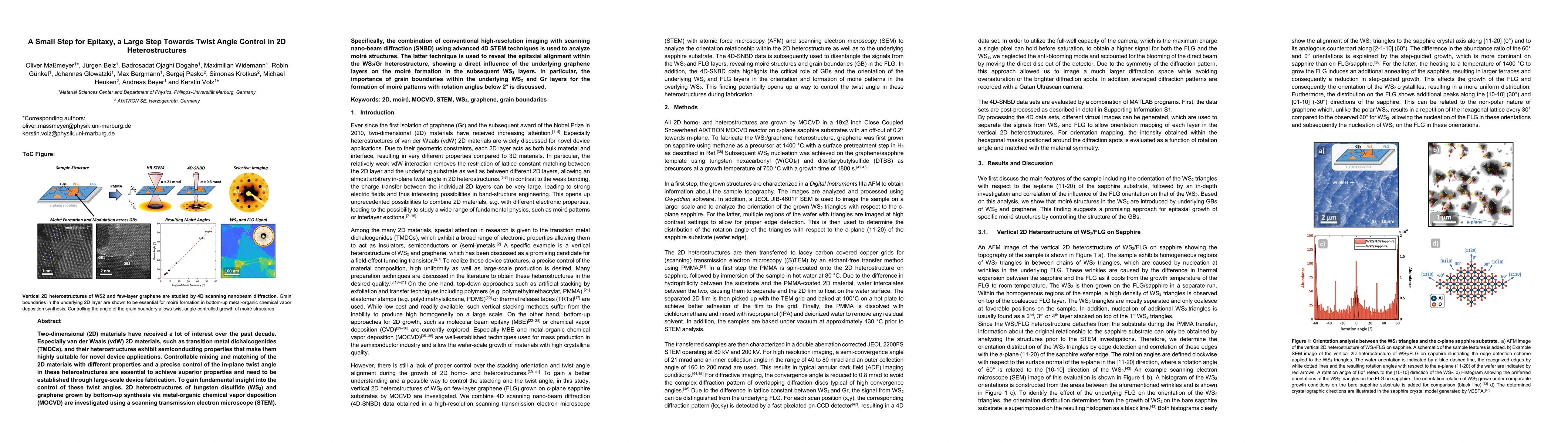
Two-dimensional (2D) materials have received a lot of interest over the past decade. Especially van der Waals (vdW) 2D materials, such as transition metal dichalcogenides (TMDCs), and their heterost...

Thumbnail for Understanding & Predicting User Lifetime with Machine Learning in an
  Anonymous Location-Based Social Network
arXiv
Understanding & Predicting User Lifetime with Machine Learning in an Anonymous Location-Based Social Network

In this work, we predict the user lifetime within the anonymous and location-based social network Jodel in the Kingdom of Saudi Arabia. Jodel's location-based nature yields to the establishment of d...

Thumbnail for Low Temperature MOCVD Synthesis of high-mobility 2D InSe
arXiv
Low Temperature MOCVD Synthesis of high-mobility 2D InSe

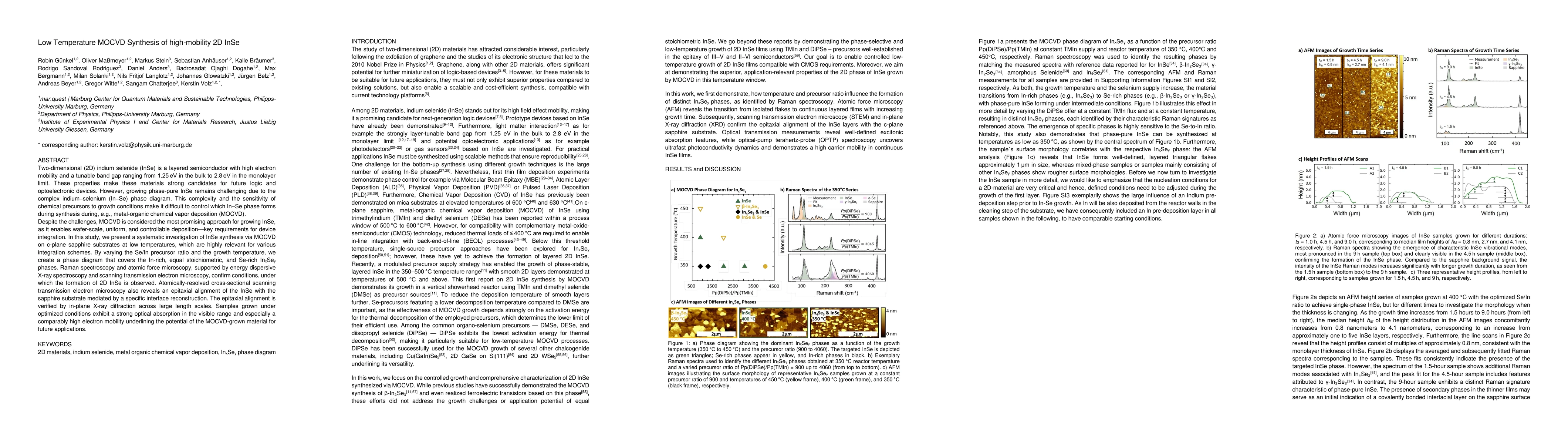
Two-dimensional (2D) indium selenide (InSe) is a layered semiconductor with high electron mobility and a tunable band gap ranging from 1.25 eV in the bulk to 2.8 eV in the monolayer limit. These prope...

Thumbnail for Localized Excitonic Emission in Wafer-Scale MOCVD-Grown GaSe 2D Nanosheets for Classical and Non-Classical Light Sources
arXiv
Localized Excitonic Emission in Wafer-Scale MOCVD-Grown GaSe 2D Nanosheets for Classical and Non-Classical Light Sources

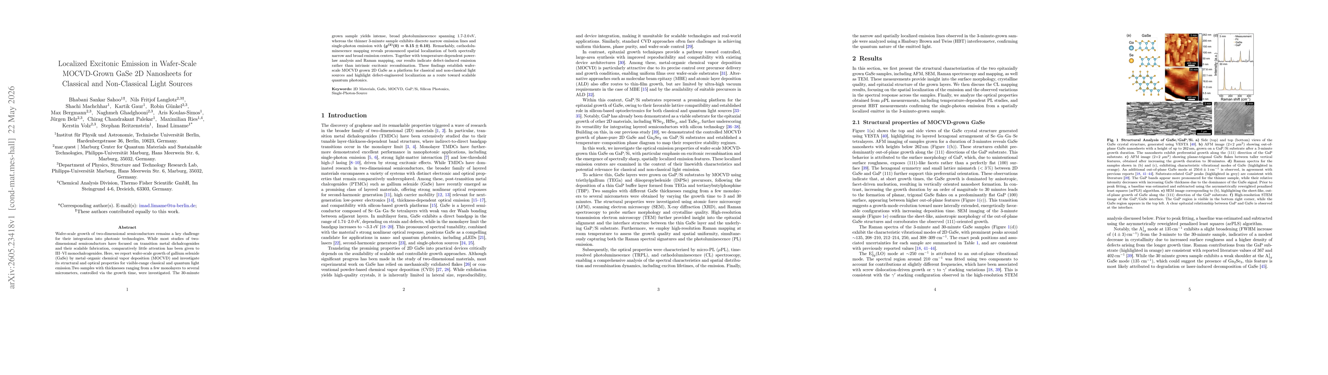
Wafer-scale growth of two-dimensional semiconductors remains a key challenge for their integration into photonic technologies. While most studies of two-dimensional semiconductors have focused on tran...

This website uses cookies to ensure you get the best experience. Learn more