Academic Profile
Statistics
Similar Authors
Papers on arXiv
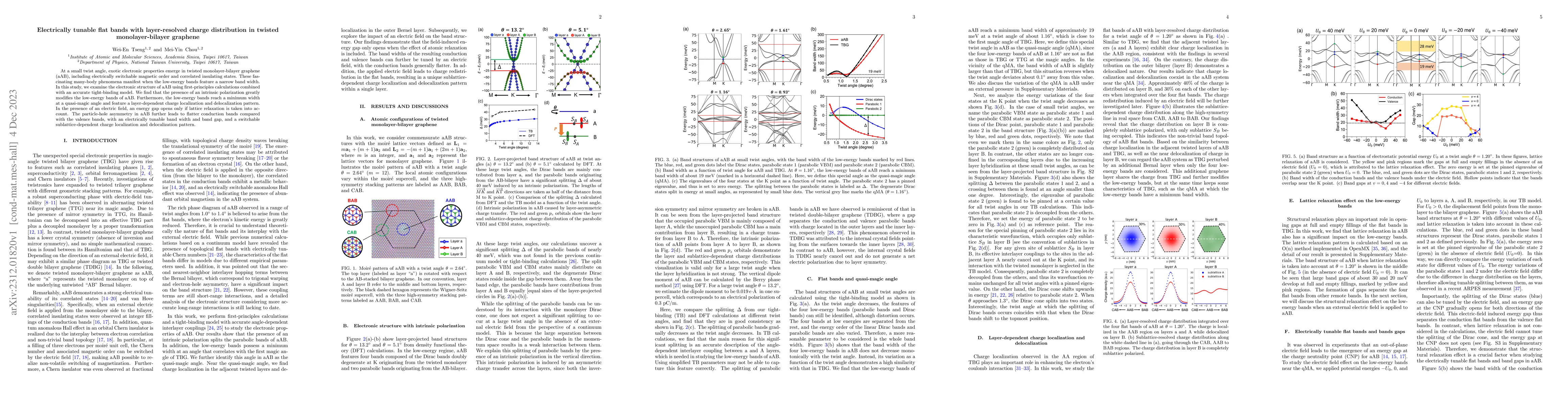
At a small twist angle, exotic electronic properties emerge in twisted monolayer-bilayer graphene (aAB), including electrically switchable magnetic order and correlated insulating states. These fasc...
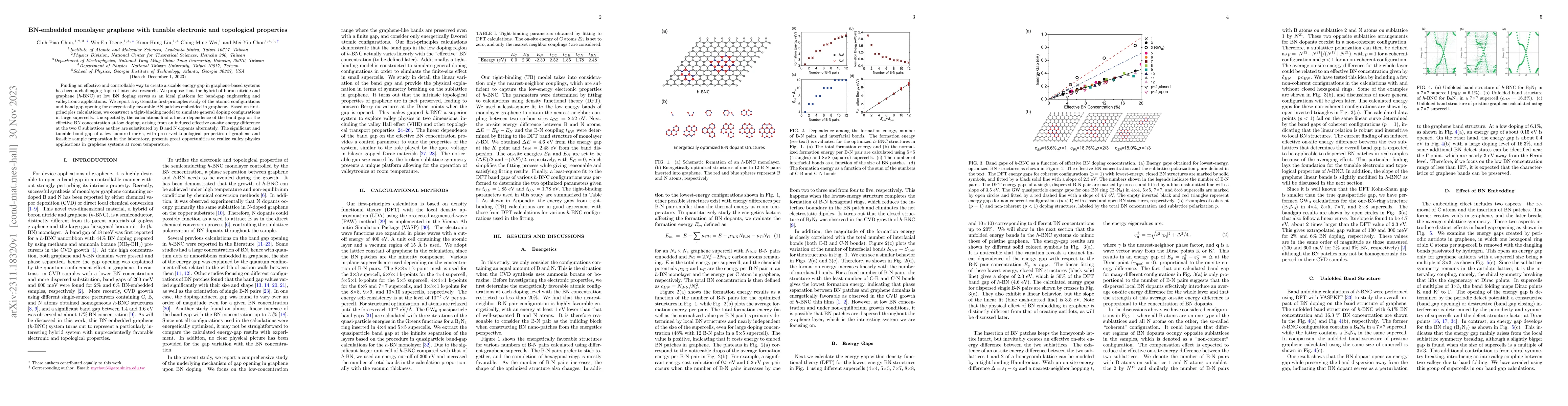
Finding an effective and controllable way to create a sizable energy gap in graphene-based systems has been a challenging topic of intensive research. We propose that the hybrid of boron nitride and...
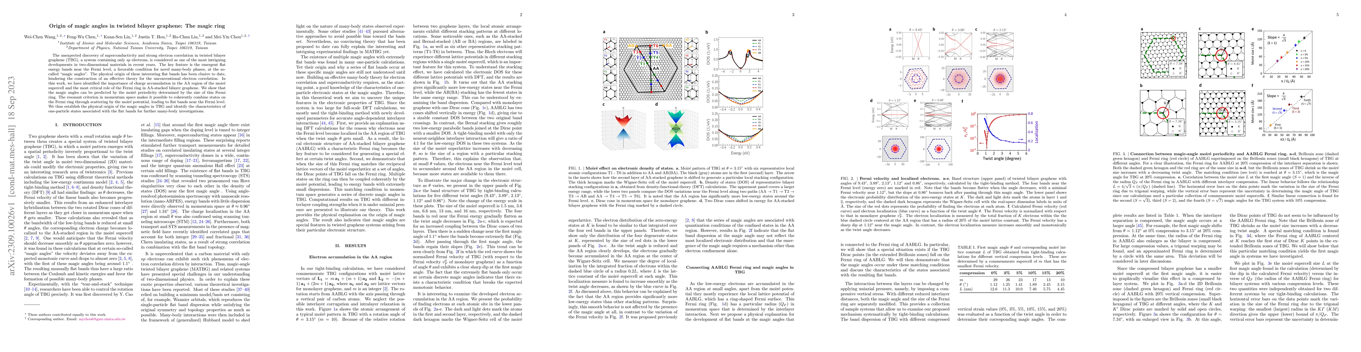
The unexpected discovery of superconductivity and strong electron correlation in twisted bilayer graphene (TBG), a system containing only sp electrons, is considered as one of the most intriguing de...
We present Gemini-NIFS, VLT-SINFONI and Keck-OSIRIS observations of near-infrared [Fe II] emission associated with the well-studied jets from three active T Tauri stars; RW Aur A, RY Tau and DG Tau ...
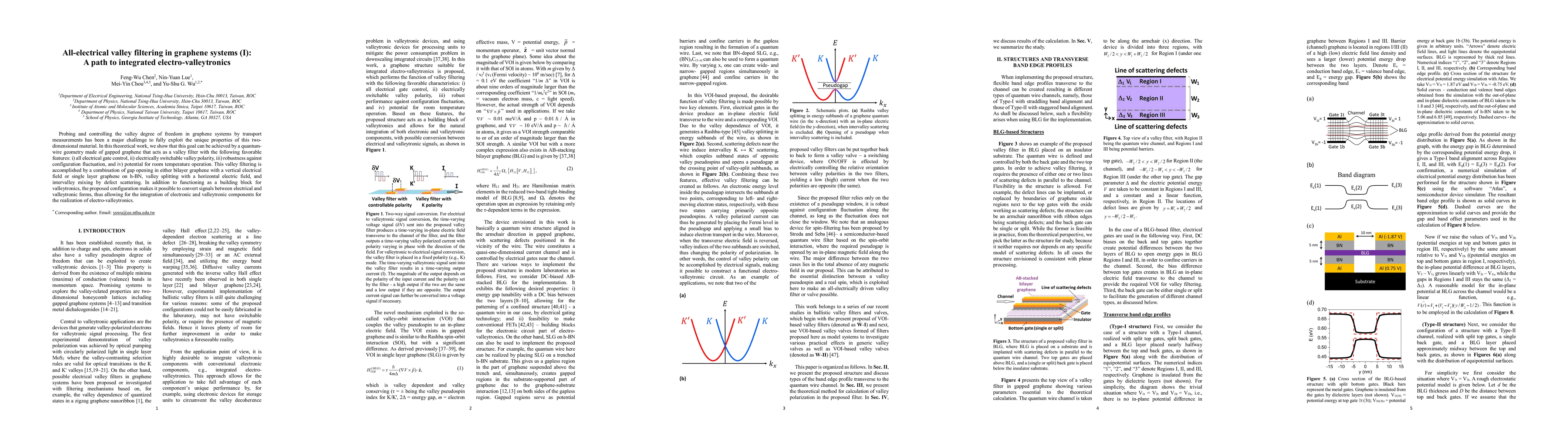
Probing and controlling the valley degree of freedom in graphene systems by transport measurements has been a major challenge to fully exploit the unique properties of this two-dimensional material....
The ability to engineer atomically thin nanoscale lateral heterojunctions (HJs) is critical to lay the foundation for future two-dimensional (2D) device technology. However, the traditional approach...
Tailoring interlayer coupling has emerged as a powerful tool to tune the electronic structure of van der Waals (vdW) bilayers. One example is the usage of the moire pattern to create controllable tw...
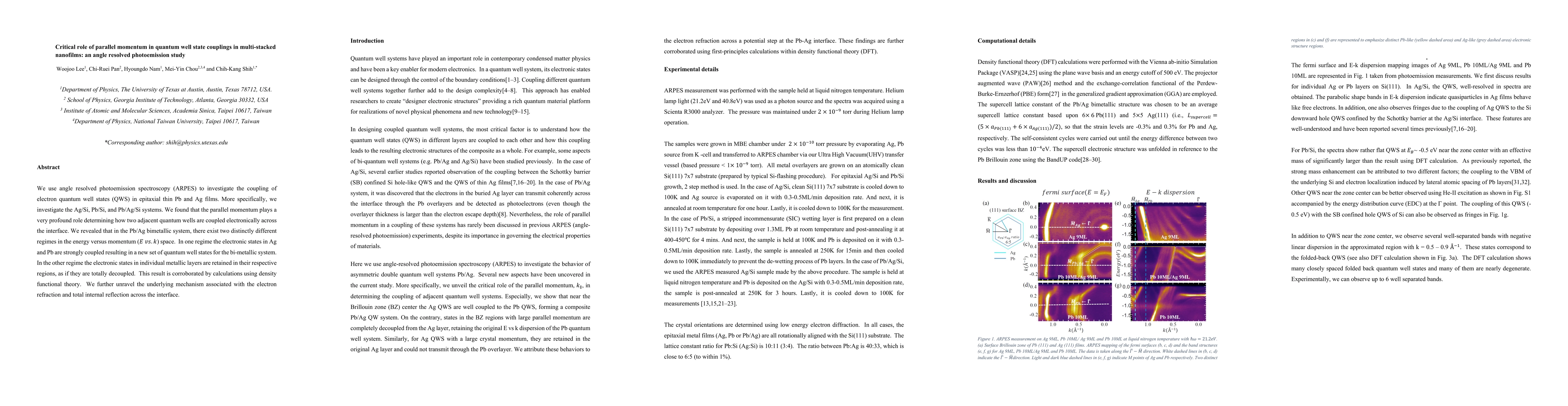
We use angle resolved photoemission spectroscopy (ARPES) to investigate the coupling of electron quantum well states (QWS) in epitaxial thin Pb and Ag films. More specifically, we investigate the Ag...
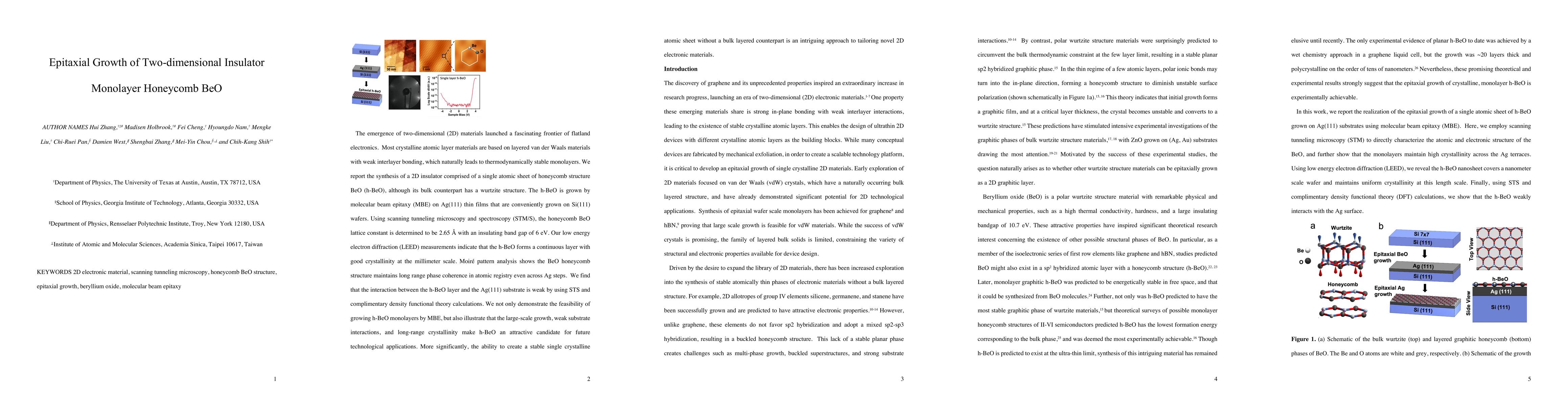
The emergence of two-dimensional (2D) materials launched a fascinating frontier of flatland electronics. Most crystalline atomic layer materials are based on layered van der Waals materials with wea...
For the active T-Taur star RW Aur A we have performed long-term (~10 yr) monitoring observations of (1) jet imaging in the [Fe II] 1.644-micron emission line using Gemini-NIFS and VLT-SINFONI; (2) o...
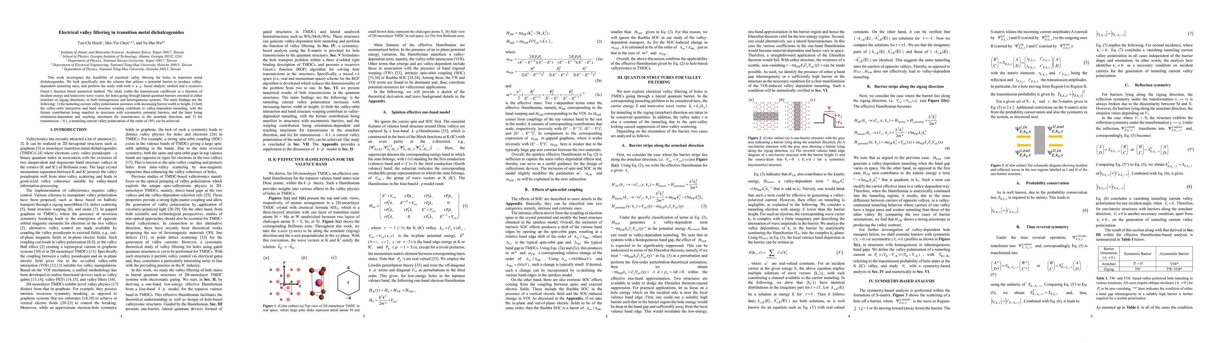
This work investigates the feasibility of electrical valley filtering for holes in transition metal dichalcogenides. We look specifically into the scheme that utilizes a potential barrier to produce...
Machine learning (ML) force fields have emerged as a powerful tool for computing materials properties at finite temperatures, particularly in regimes where traditional phonon-based perturbation theori...