Academic Profile
Statistics
Similar Authors
Papers on arXiv
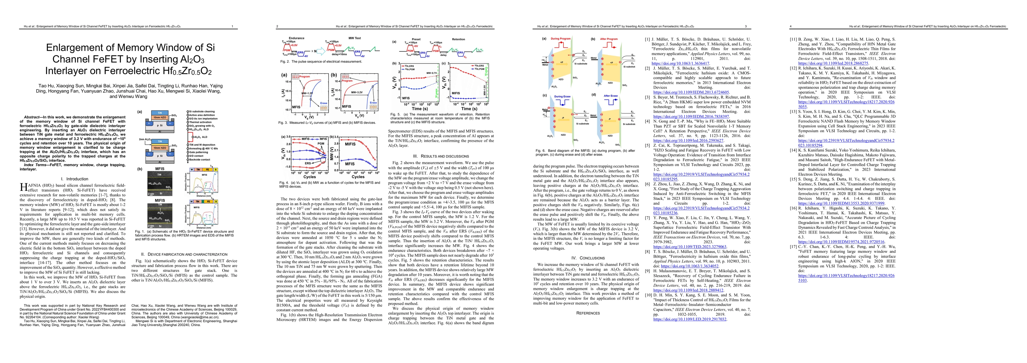
In this work, we demonstrate the enlargement of the memory window of Si channel FeFET with ferroelectric Hf0.5Zr0.5O2 by gate-side dielectric interlayer engineering. By inserting an Al2O3 dielectric...
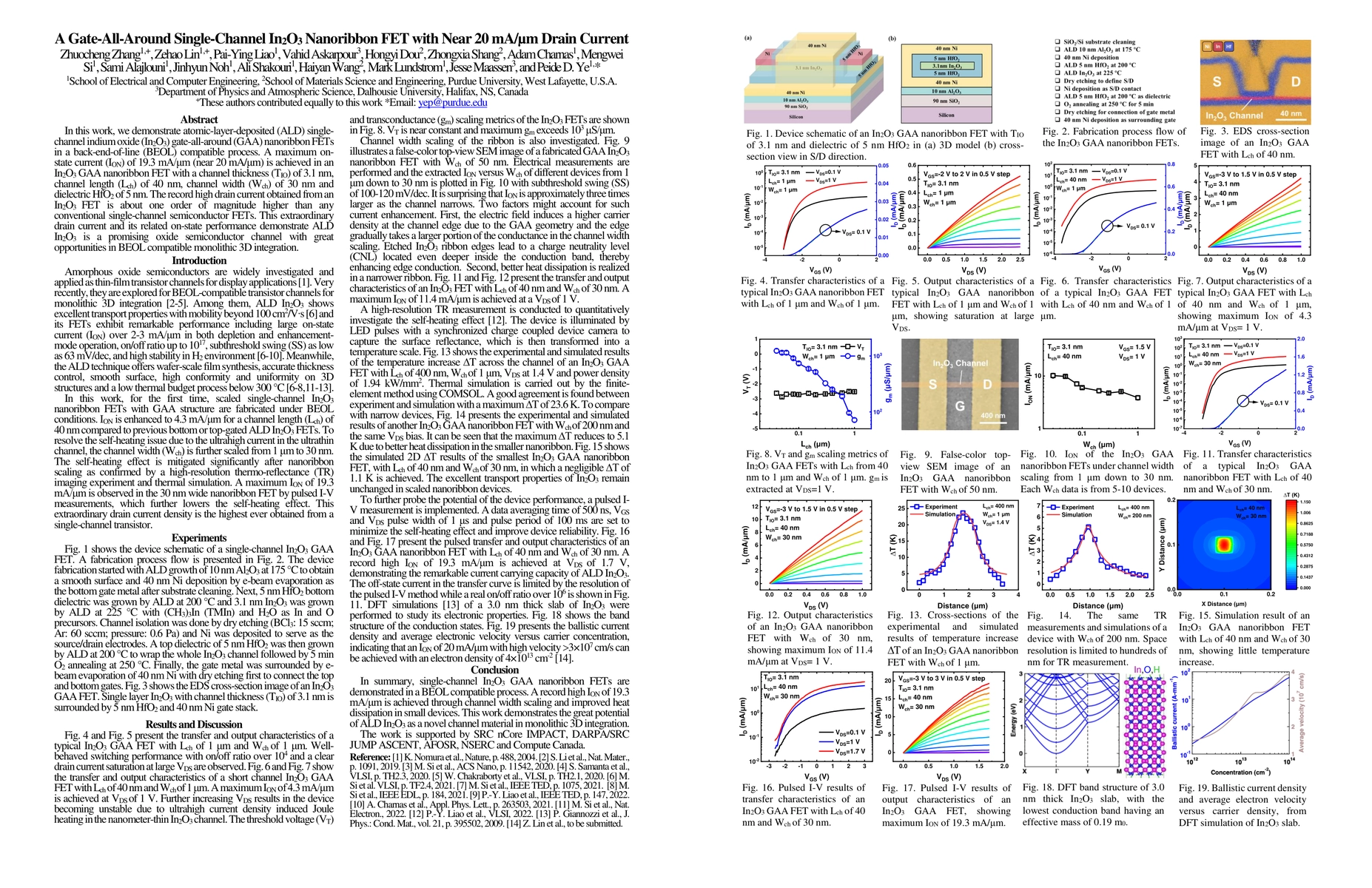
In this work, we demonstrate atomic-layer-deposited (ALD) single-channel indium oxide (In2O3) gate-all-around (GAA) nanoribbon FETs in a back-end-of-line (BEOL) compatible process. A maximum on-stat...
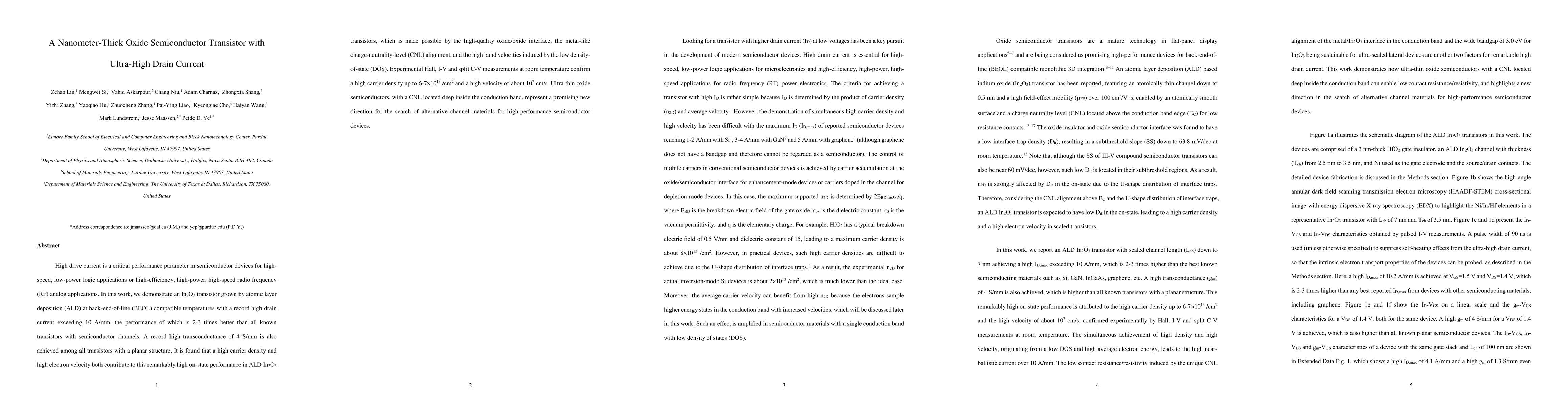
High drive current is a critical performance parameter in semiconductor devices for high-speed, low-power logic applications or high-efficiency, high-power, high-speed radio frequency (RF) analog ap...
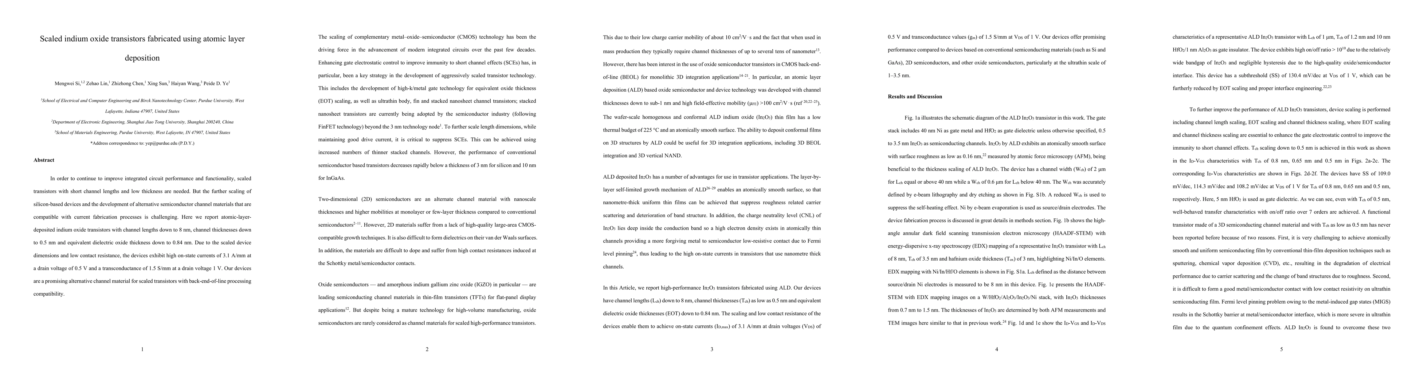
In order to continue to improve integrated circuit performance and functionality, scaled transistors with short channel lengths and low thickness are needed. But the further scaling of silicon-based...
The van der Waals layered material CuInP2S6 features interesting functional behavior, including the existence of four uniaxial polarization states, polarization reversal against the electric field t...
Tellurium (Te) is a narrow bandgap semiconductor with a unique chiral crystal structure. The topological nature of electrons in the Te conduction band can be studied by realizing n-type doping using...
Ferroelectric field-effect transistors (Fe-FETs) with ferroelectric hafnium oxide (FE HfO2) as gate insulator are being extensively explored as a promising device candidate for three-dimensional (3D...
We investigate the polarization switching mechanism in ferroelectric-dielectric (FE-DE) stacks and its dependence on the dielectric thickness (TDE). We fabricate HZO-Al2O3 (FE-DE) stack and experime...
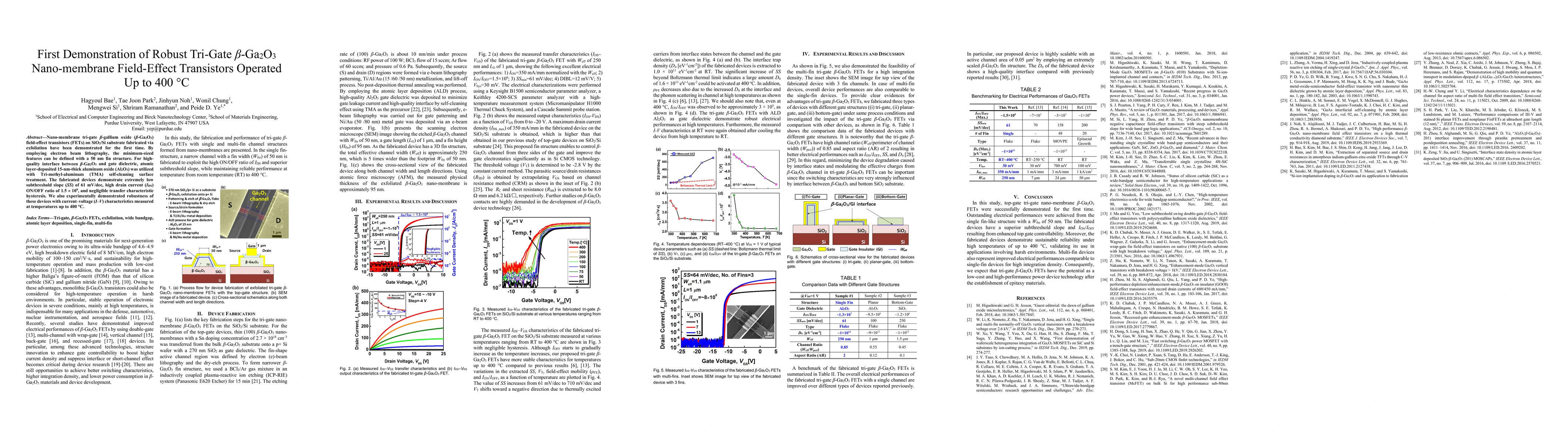
Nano-membrane tri-gate beta-gallium oxide (\b{eta}-Ga2O3) field-effect transistors (FETs) on SiO2/Si substrate fabricated via exfoliation have been demonstrated for the first time. By employing elec...
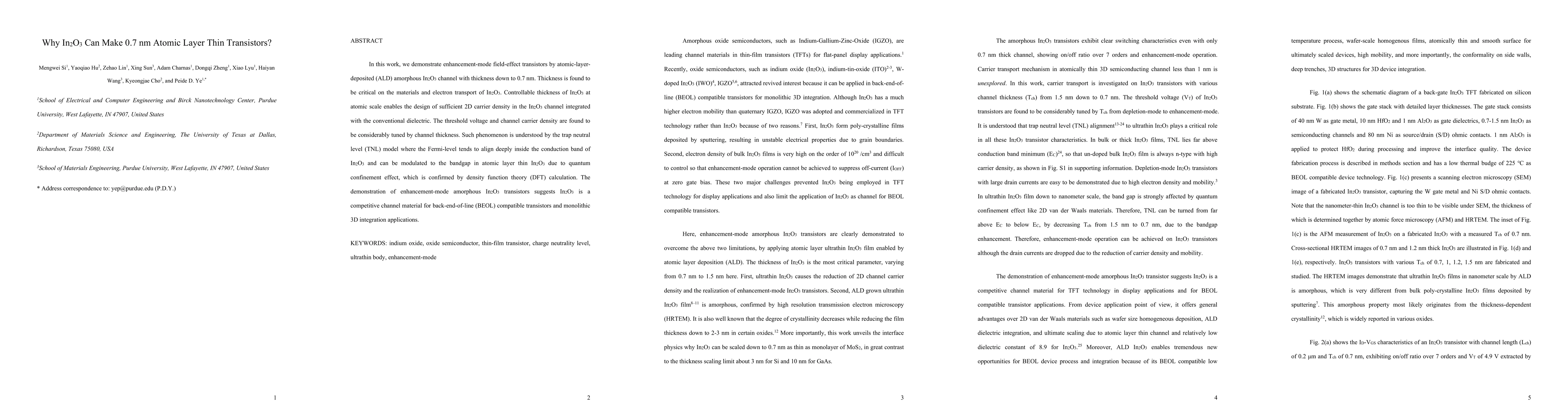
In this work, we demonstrate enhancement-mode field-effect transistors by atomic-layer-deposited (ALD) amorphous In2O3 channel with thickness down to 0.7 nm. Thickness is found to be critical on the...
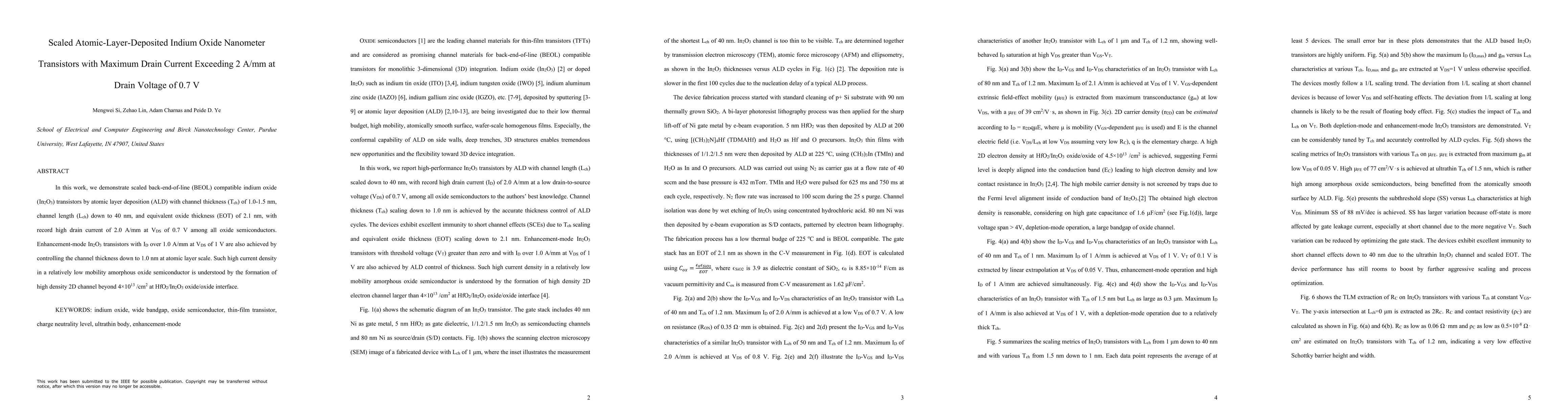
In this work, we demonstrate scaled back-end-of-line (BEOL) compatible indium oxide (In2O3) transistors by atomic layer deposition (ALD) with channel thickness (Tch) of 1.0-1.5 nm, channel length (L...
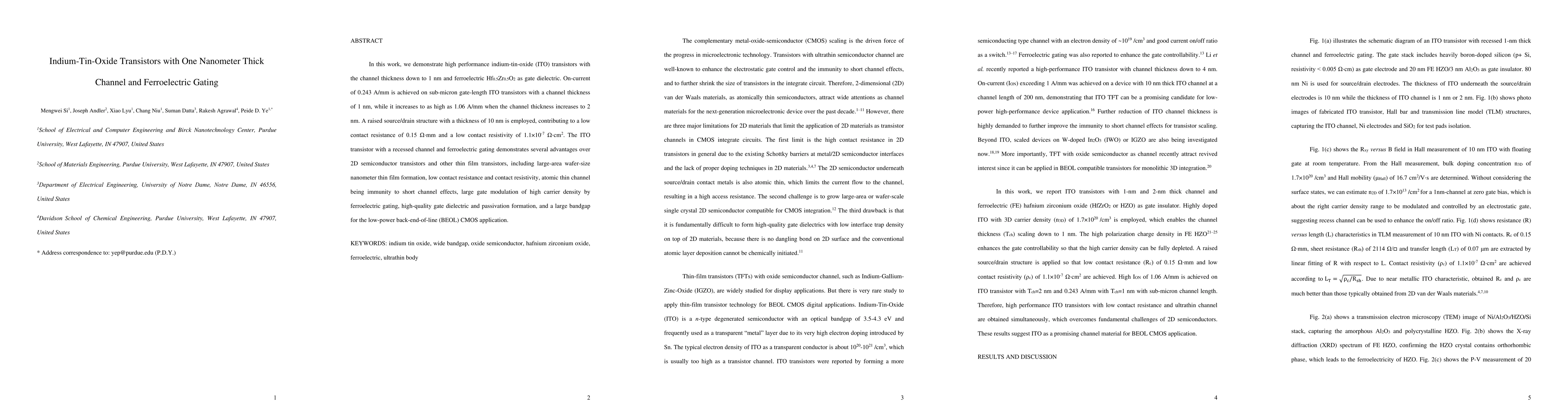
In this work, we demonstrate high performance indium-tin-oxide (ITO) transistors with the channel thickness down to 1 nm and ferroelectric Hf0.5Zr0.5O2 as gate dielectric. On-current of 0.243 A/mm i...
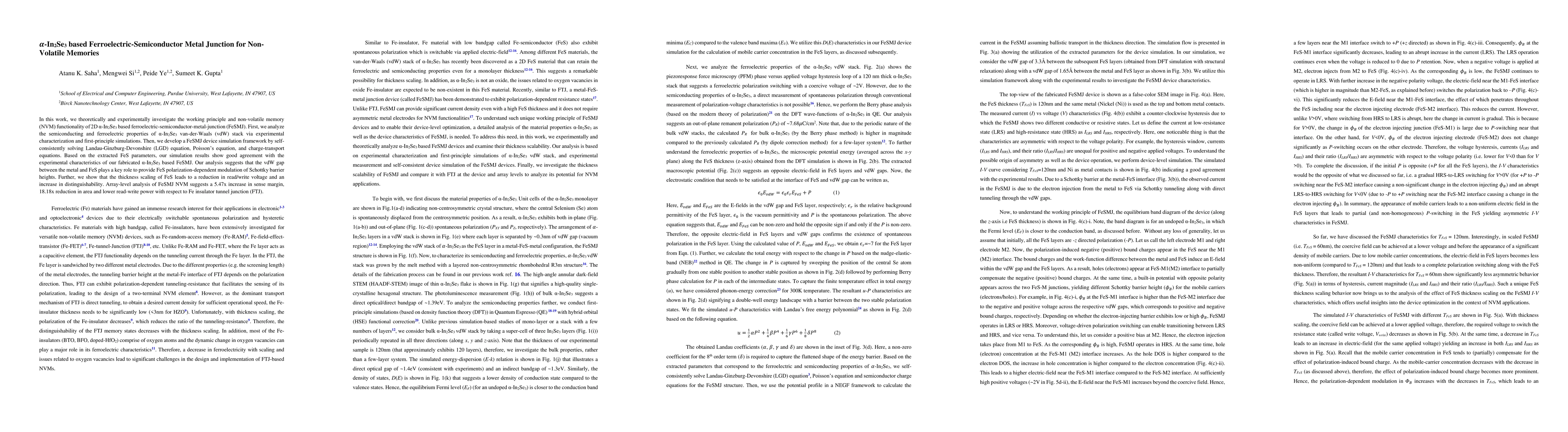
In this work, we theoretically and experimentally investigate the working principle and non-volatile memory (NVM) functionality of 2D $\alpha$-In$_2$Se$_3$ based ferroelectric-semiconductor-metal-ju...
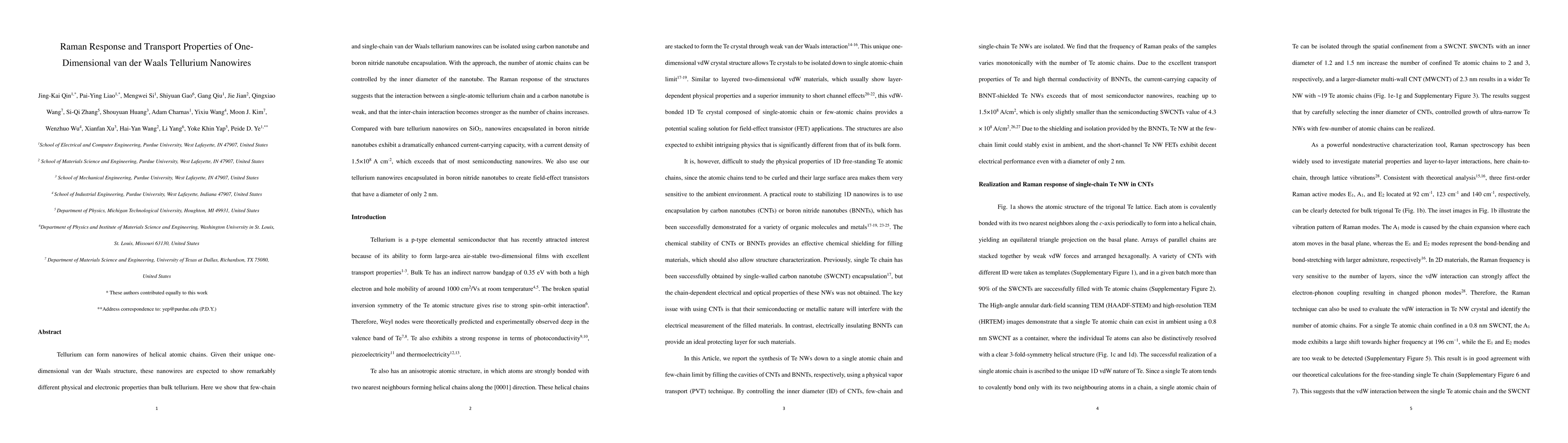
Tellurium can form nanowires of helical atomic chains. Given their unique one-dimensional van der Waals structure, these nanowires are expected to show remarkably different physical and electronic p...
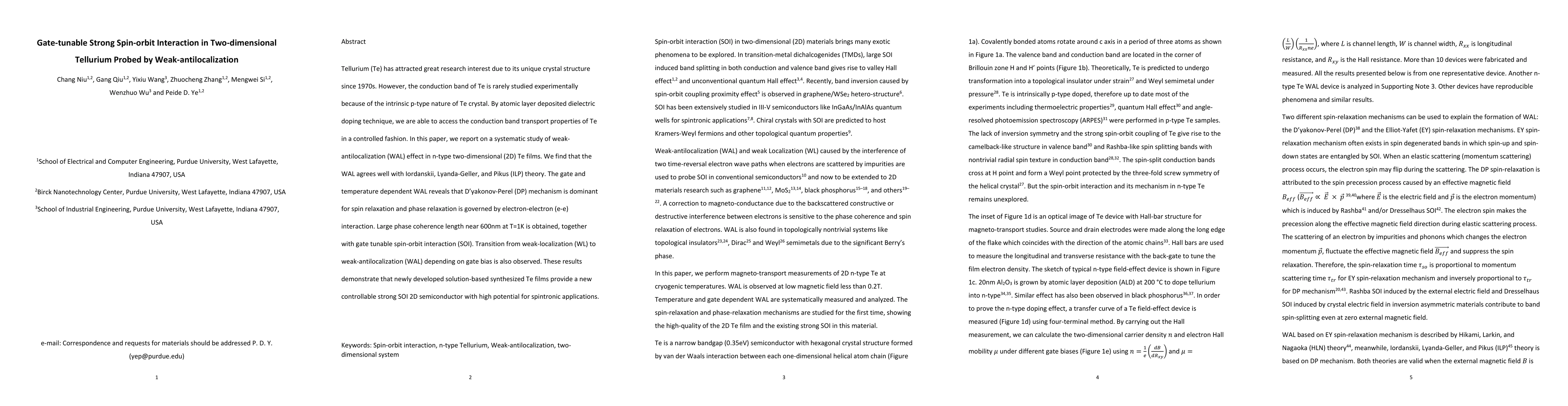
Tellurium (Te) has attracted great research interest due to its unique crystal structure since 1970s. However, the conduction band of Te is rarely studied experimentally because of the intrinsic p-t...
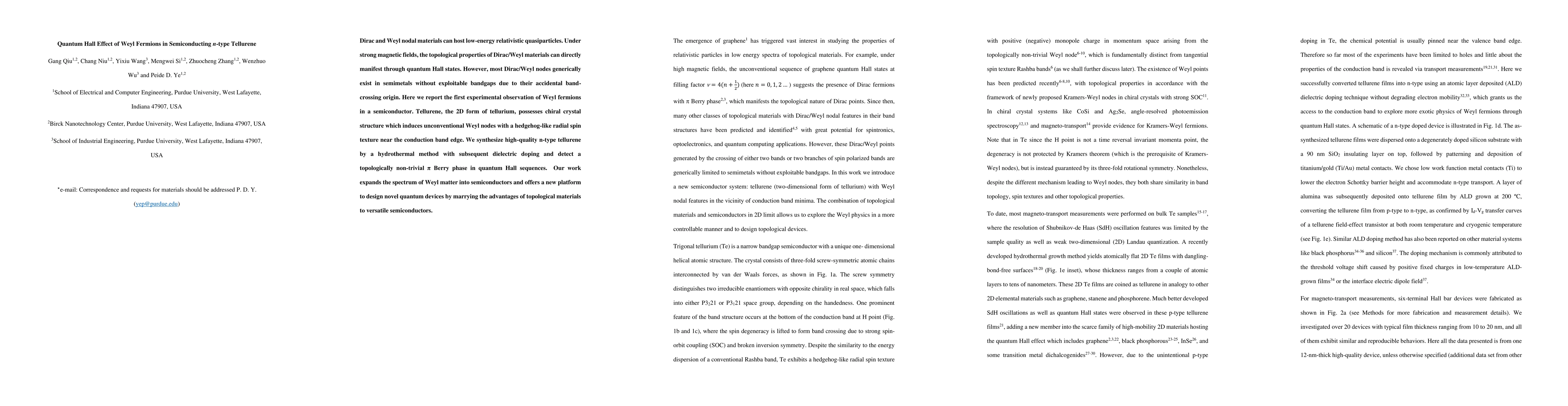
Dirac and Weyl nodal materials can host low-energy relativistic quasiparticles. Under strong magnetic fields, the topological properties of Dirac/Weyl materials can directly manifest through quantum...
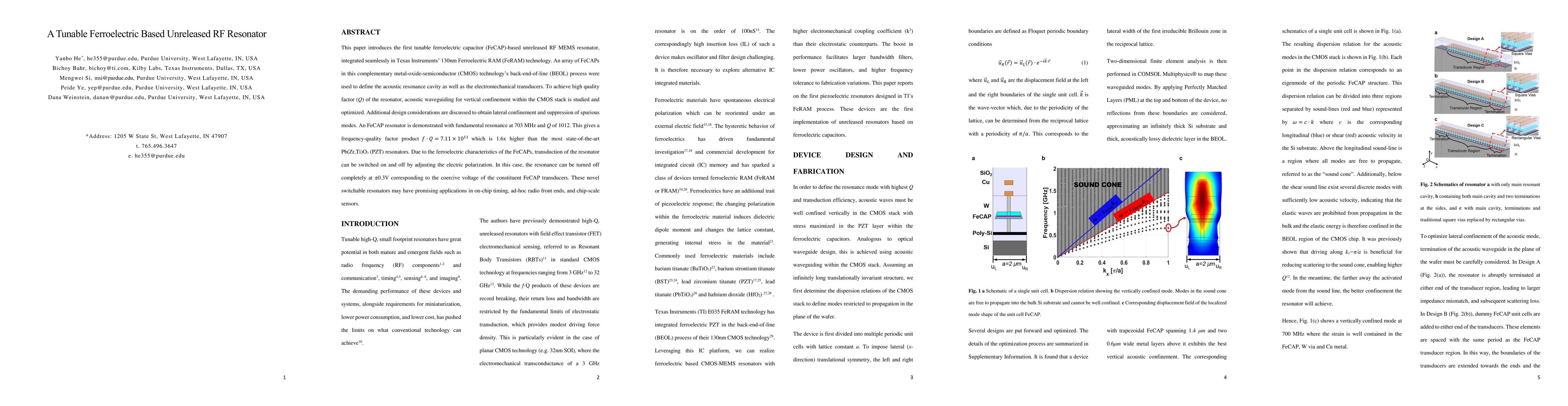
This paper introduces the first tunable ferroelectric capacitor (FeCAP) based unreleased RF MEMS resonator, integrated seamlessly in Texas Instruments' 130nm Ferroelectric RAM (FeRAM) technology. An...
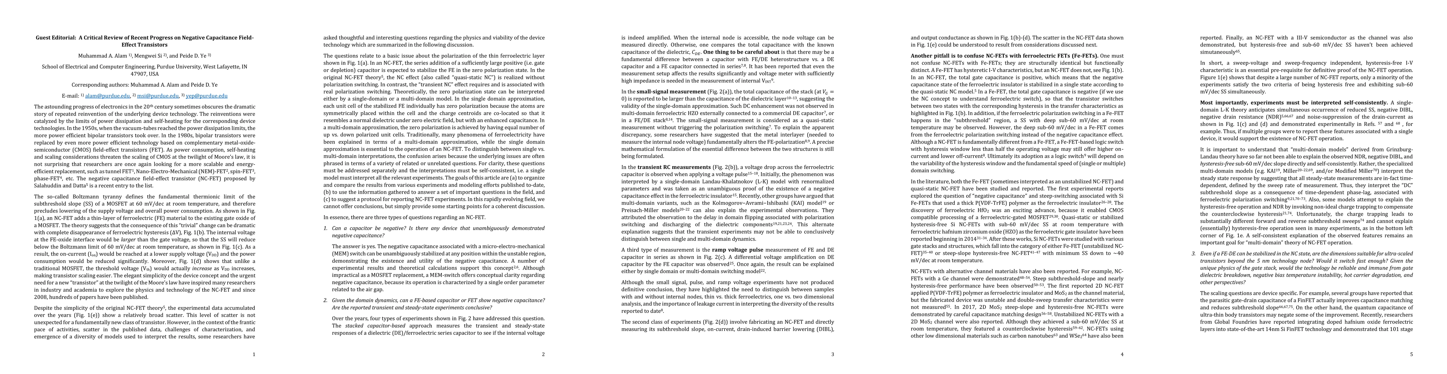
The elegant simplicity of the device concept and the urgent need for a new "transistor" at the twilight of Moore's law have inspired many researchers in industry and academia to explore the physics ...
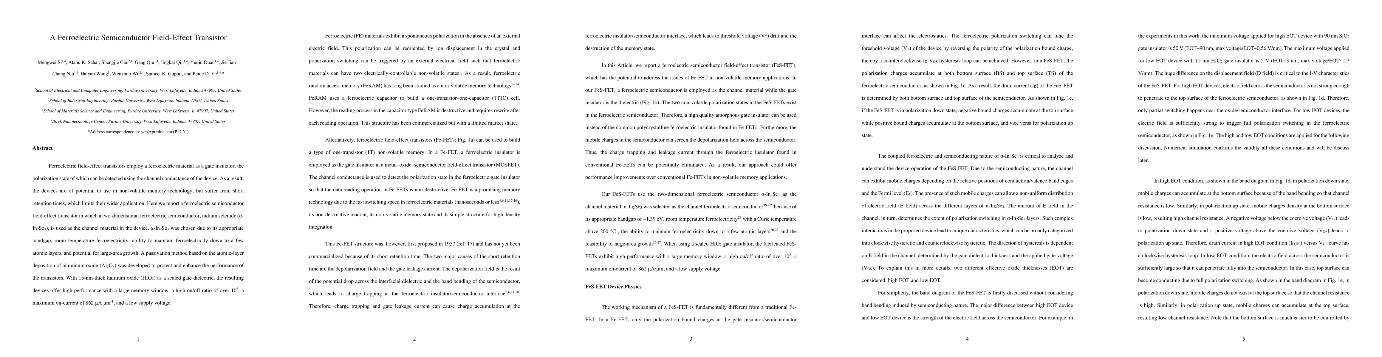
Ferroelectric field-effect transistors employ a ferroelectric material as a gate insulator, the polarization state of which can be detected using the channel conductance of the device. As a result, ...
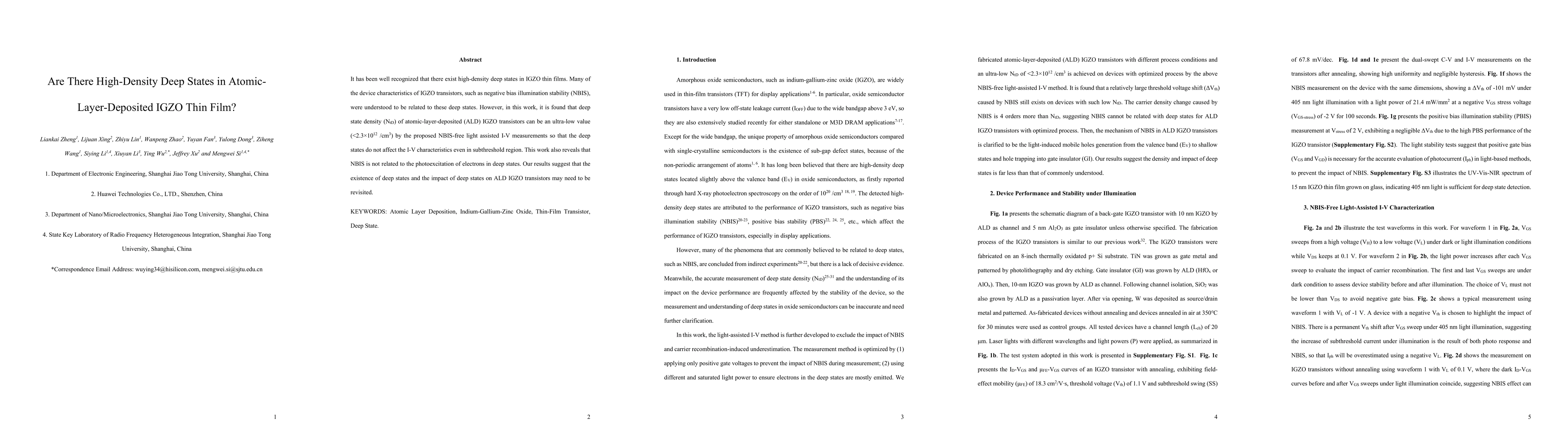
It has been well recognized that there exist high-density deep states in IGZO thin films. Many of the device characteristics of IGZO transistors, such as negative bias illumination stability (NBIS),we...
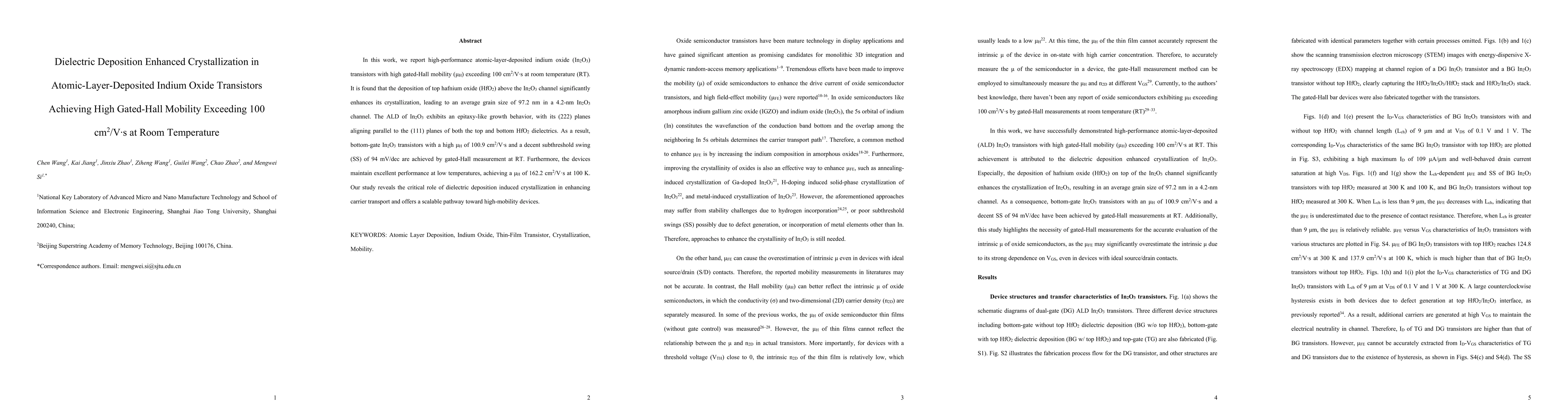
In this work, we report high-performance atomic-layer-deposited indium oxide (In2O3) transistors with high gated-Hall mobility ({\mu}H) exceeding 100 cm2/Vs at room temperature (RT). It is found that ...
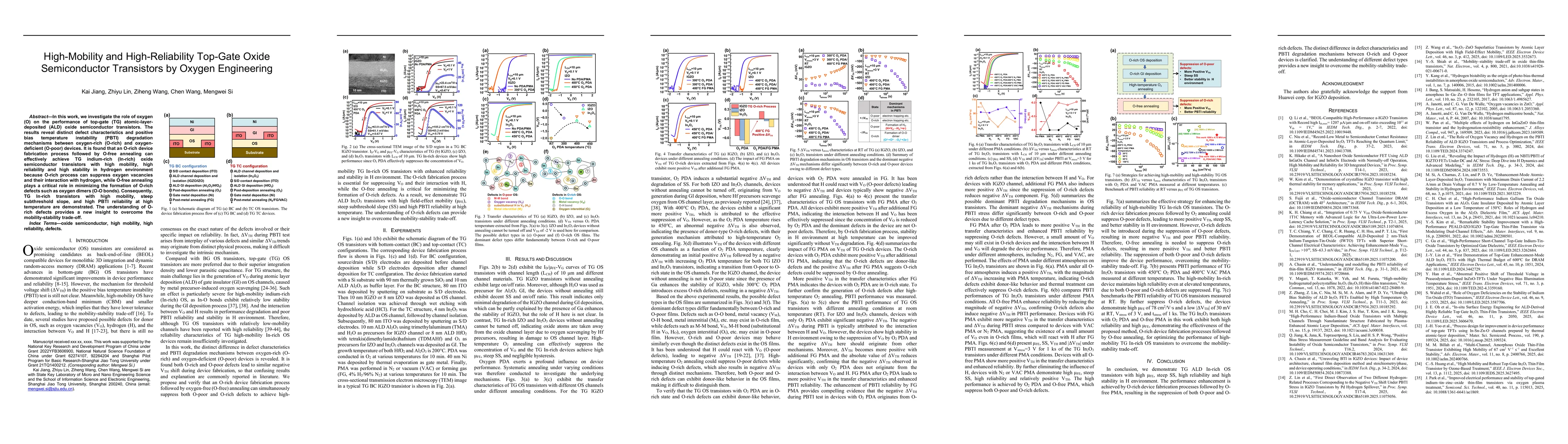
In this work, we investigate the role of oxygen (O) on the performance of top-gate (TG) atomic-layer-deposited (ALD) oxide semiconductor transistors. The results reveal distinct defect characteristics...
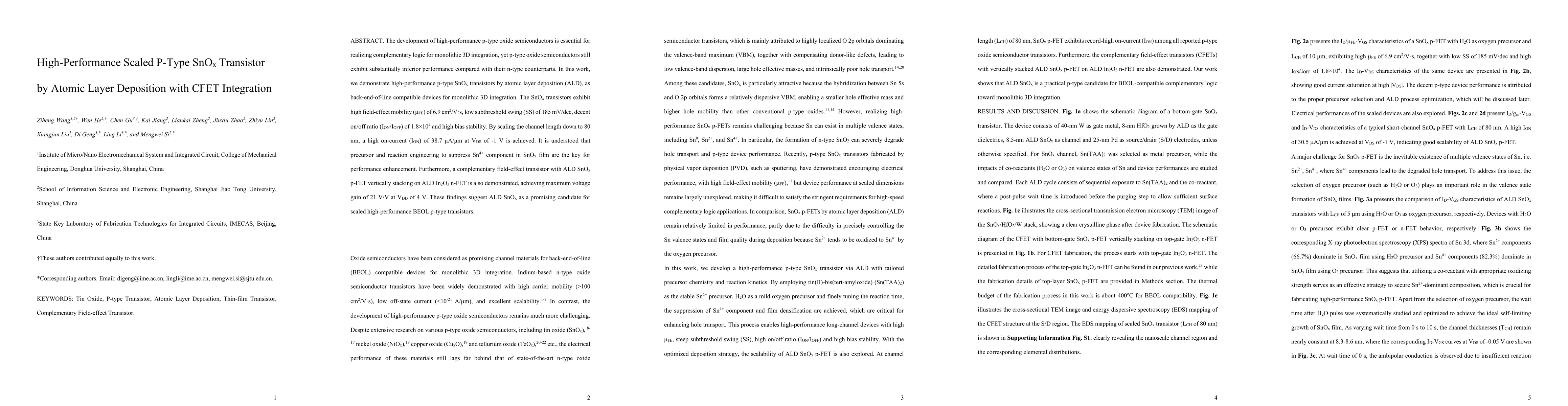
The development of high-performance p-type oxide semiconductors is essential for realizing complementary logic for monolithic 3D integration, yet p-type oxide semiconductors still exhibit substantiall...
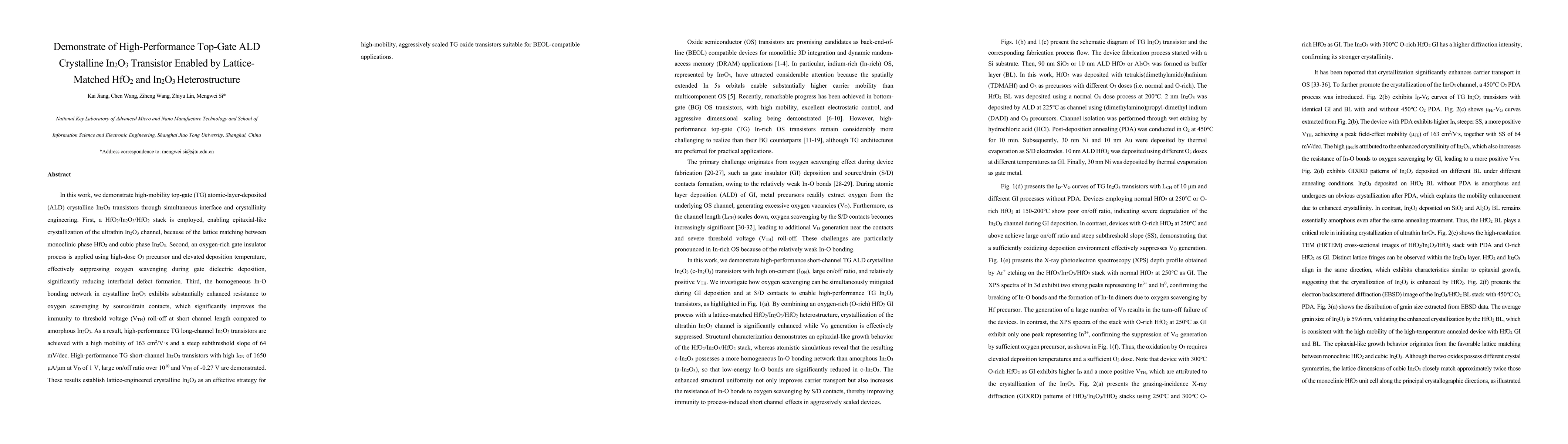
In this work, we demonstrate high-mobility top-gate (TG) atomic-layer-deposited (ALD) crystalline In2O3 transistors through simultaneous interface and crystallinity engineering. First, a HfO2/In2O3/Hf...
In this work, magneto-transport measurements, including Hall effects and magnetoresistance (MR) at various temperatures, are employed to directly probe the electron transport properties in crystalline...